Odroid-N2 SBC launches at $63 with new Cortex-A73 SoC

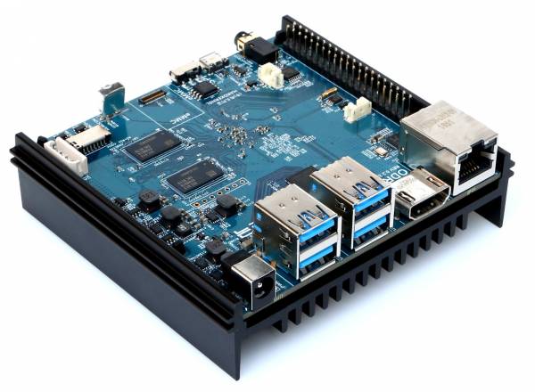
ODROID-N2 is a new generation single board computer that is more powerful, more stable, and faster performing than ODROID-N1. The main CPU of the N2 is based on big.Little architecture which integrates a quad-core ARM Cortex-A73 CPU cluster and a dual core Cortex-A53 cluster with a new generation Mali-G52 GPU. Thanks to the modern 12nm silicon technology, the A73 cores runs at 1.8Ghz without thermal throttling using the stock metal-housing heatsink allowing a robust and quiet computer.

The CPU multi-core performance is around 20% faster and the 4GByte DDR4 RAM is 35% faster than the N1. The N2’s DDR4 RAM is running at 1320Mhz while N1’s DDR3 was running at 800Mhz. The large metal housing heatsink is designed to optimize the CPU and RAM heat dissipation and minimize throttling. The CPU is placed on the bottom side of the PCB to establish great thermal characteristics.

ODROID-N2 block diagram

The specs for the Odroid-N2 appear to be the same as those we detailed in February when the SBC was formally announced.

Specifications listed for the Odroid-N2 include:

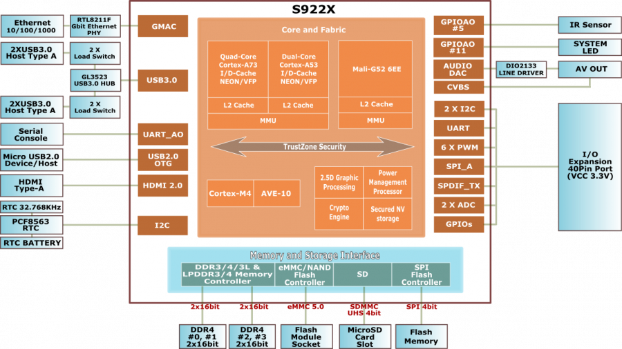
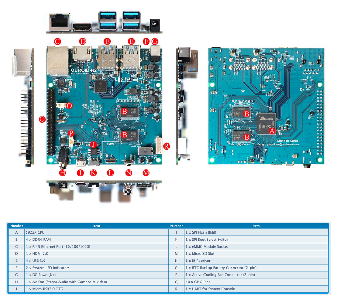
  • Processor — Amlogic S922X (4x Cortex-A73 @ 1.8GHz, 2x Cortex-A53 @ 1.9GHz); 12nm fab; Mali-G52 GPU with 6x 846MHz EEs
  • Memory/storage:
    • 2GB or 4GB DDR4 (1320MHz, 2640MT/s) 32-bit RAM
    • eMMC socket with optional 8GB to 128GB
    • MicroSD slot with UHS-1 SDR104 support
    • 8MB SPI flash with boot select switch and Petitboot app
  • Wireless — Optional USB WiFi adapter
  • Networking — Gigabit Ethernet port (Realtek RTL8211F); about 1Gbps
  • Media I/O:
    • HDMI 2.1 port for up to 4K@60Hz with HDR, CEC, EDID
    • Composite video jack with stereo line-out and 384Khz/32bit audio DAC
    • SPDIF audio via 40-pin
  • Other I/O:
    • 4x USB 3.0 host ports (340MB/s typical)
    • Micro-USB 2.0 OTG port (no power)
    • Serial console interface
    • Fan connector
  • Expansion — 40-pin GPIO header (25x GPIO, 2x i2C, 2x ADC, 6x PWM, SPI, UART, SPDIF, various power signals, etc.)
  • Other features — RTC (NXP PCF8563) with battery connector; IR receiver; metal heatsink; 2x LEDs; optional $4 acrylic case
  • Power — 7.5-20V DC jack; 12V/2A adapter recommended; consumption: 1.8W idle to 5.5W stress
  • Dimensions — 90 x 90 x 17mm
  • Operating system — Ubuntu 18.04 LTS with Kernel 4.9.152 LTS and Android 9 Pie BSPs

The Odroid-N2 is on sale for $63 (2GB RAM) or $79 (4GB) with shipments beginning April 3. More information may be found on Hardkernel’s $63 (2GB RAM) and $79 (4GB) shopping pages and the Odroid-N2 wiki.

Avnet Introduces Ultra96-V2 Development Board with certified WiFi

Just one year after introducing its successful Ultra96 development board, Avnet, a leading global technology solutions provider, has released the new Ultra96-V2 to power industrial-grade Artificial Intelligence (AI) and Internet of Things (IoT) applications. Complete with an updated radio module that enables engineers to extend their reach into new markets, Avnet’s Ultra96-V2 is an ideal platform for smart home, automotive, industrial controls and many other applications.

The Ultra96-V2 board offers engineers and makers a very price competitive development platform for rapidly prototyping the next breakthroughs in AI, IoT, robotics and beyond,” said Bryan Fletcher, technical marketing director, Avnet. “Avnet is proud to support the 96Boards initiative by bringing new performance, additional power-savings, and programmable logic advances to this community of Arm experts and enthusiasts.

The Ultra96-V2 enhances the capabilities of the 96Boards community with a range of peripherals and acceleration engines in the programmable logic not available from other offerings. Like its predecessor, the Ultra96-V2 is an Arm-based, Xilinx Zynq UltraScale+™ MPSoC development board built on the Linaro 96Boards Consumer Edition (CE) specification. The 96Boards are open source development platforms that can be used by system software developers for software applications, hardware devices and kernel programming for operating systems.

Ultra96-V2 block diagram

Engineers can now extend the market reach of their innovations globally with the Ultra96-V2’s new feature – a Wi-Fi / Bluetooth radio module from Microchip that is Agency Certified in more than 75 countries. Wireless options include 802.11b/g/n WiFi and Bluetooth 5 Low Energy support.

The Ultra96-V2 features include:

  • Xilinx Zynq UltraScale+ MPSoC ZU3EG A484
  • Micron 2 GB (512M x32) LPDDR4 Memory
  • Delkin 16 GB microSD card + adapter
  • PetaLinux environment available for download
  • Microchip Wi-Fi / Bluetooth
  • Mini DisplayPort (MiniDP or mDP)
  • 1x USB 3.0 Type Micro-B upstream port
  • 2x USB 3.0, 1x USB 2.0 Type A downstream ports
  • 40-pin 96Boards Low-speed expansion header
  • 60-pin 96Boards High-speed expansion header
  • 85mm x 54mm form factor
  • Linaro 96Boards Consumer Edition compatible

The platform comes as a complete development kit including:

  • Ultra96-V2 development board
  • 16 GB microSD card + adapter
  • Voucher for SDSoC license from Xilinx
  • Quick-start instruction card

Avnet also updated all components on the Ultra96-V2 to allow industrial temperature grade options so that the board can operate in harsh industrial applications. Additional power control and monitoring is also possible with Infineon’s integrated power management ICs (PMICS) designed for tight board space requirements.

Ultra96-V2 allows the 96Boards community members to explore programmable logic to accelerate software. Software engineers’ C, C++, and OpenCL algorithms can be compiled into the FPGA portion of the Zynq UltraScale+ MPSoC to achieve massive parallelism and really high performance,

said Tomas Evensen, CTO of Embedded Software at Xilinx.

The Ultra96-V2 development board will be available in May for $249. More information may be found on Avnet’s Ultra96-V2 product page and shopping page.

Tiny, octa-core Arm module (Qualcomm SDA660) targets AI on the edge

Designed for use in 4K Cameras, Gaming, Digital Signage, and other Consumer and Industrial IoT Devices.

Intrinsyc Technologies Corporation, a leading provider of solutions for the development and production of embedded and Internet of Things (IoT) products, today announced the availability of the Open-Q™ 660 µSOM (micro System on Module) and Development Kit.

Intrinsyc’s Open-Q™ 660 µSOM is an ultra-compact (50mm x 25mm) production-ready embedded computing module.  The SOM is powered by the Qualcomm® SDA660 system on chip (SoC), a product of Qualcomm Technologies, Inc., and is designed to support high-performance, intelligent, on-device processes utilizing heterogenous compute capabilities to power a variety of high-performance consumer and industrial IoT devices.

Open-Q 660 μSOM, back
Open-Q 660 μSOM, front

The Qualcomm SDA660 features eight Qualcomm® Kryo™ 64-bit 260 cores that are divided in two clusters – a fast cluster of four cores with up to 2.2 GHz and a power saving efficiency cluster of four cores with up to 1.8 GHz. Additional high-end features in Qualcomm SDA660 mobile platform include the powerful Qualcomm® Artificial Intelligence (AI) Engine), Qualcomm Spectra™ ISP, and Qualcomm® Hexagon™ 680 DSP with Hexagon Vector eXtensions (HVX), designed to support Caffe2 and Tensorflow for machine learning and image processing.

Intrinsyc’s Open-Q™ 660 µSOM is an ideal platform to power the growing demand for consumer and industrial IoT devices capable of artificial intelligence and machine learning,” said Cliff Morton, Vice President, Solutions Engineering, Intrinsyc. “To assist with integration of our System on Modules into customer products, Intrinsyc offers strong capabilities in all phases of product development. Services include everything from electrical and mechanical design to software development, including camera and audio tuning, artificial intelligence, power optimization, device management, security, and more.

We are proud to see Intrinsyc’s new micro-SOM product being powered by the Qualcomm SDA660,

said Jeffery Torrance, vice president, business development, Qualcomm Technologies, Inc.

Qualcomm Technologies is driving the Internet of Things forward with our cutting-edge compute and connectivity technologies, and we are honored to enable a bright future of IoT devices along with Intrinsyc.

Open-Q™ 660 µSOM Specifications:

  • Qualcomm® SDA660 SoC:
    • Qualcomm® Kryo™ 260 CPU (up to 2.2GHz)
    • Qualcomm® Adreno™ 512 GPU
    • Qualcomm® Hexagon™ 680 DSP with Hexagon Vector extensions
  • System Memory: eMCP – 4GB LPDDR4x RAM + 32GB eMMC storage
  • Wireless Connectivity: Wi-Fi 802.11a/b/g/n/ac 2.4/5Ghz 2×2 MU-MIMO + Bluetooth 5.x
  • Display Interfaces:
    • 2x MIPI 4-lane DSI + touch panel
    • VESA DisplayPort v1.3 via USB Type-C, up to 4K30 or 2K60
  • Camera Interfaces:
    • 3x MIPI CSI D-PHY1.2 camera ports
    • Dual 14-bit Qualcomm Spectra™ ISP supports up to 2 x 16MP cameras
  • Video Performance:
    • Encode: 4K30 HEVC/H.264/VP8/MPEG4
    • Decode: 4K30 8-bit: H.264/VP8/VP9, 4K30 10-bit: HEVC
    • Concurrent: 1080p60 Decode + 1080p30 Encode
  • Audio Interfaces:
    • SLIMBus to support Qualcomm® WCD9335 audio codec (off-SOM)
    • Multi-channel I2S digital audio interface
  • I/O Interfaces:
    • 1x USB3.1 Gen1 Type C
    • 1x USB 2.0 Host
    • 1x SDIO 4-bit interface
    • General purpose UART, I2C, SPI
    • Sensor interface – SPI, UART, I2C to sensor DSP core
  • Power: Integrated battery management on SOM
  • Size: 50mm x 25mm
  • Operating System: Android 9 Pie

Developement Kit

To help IoT device makers accelerate time to market, Intrinsyc provides the Open-Q™ 660 µSOM Development Kit, as well as turnkey product development services, driver and application software development, technical support, and documentation.

Intrinsyc’s Open-Q 660 µSOM Development Kit is a full-featured development platform including the software tools and accessories required to immediately begin development. The development kit marries the production-ready Open‐Q™ 660 µSOM with a carrier board providing numerous expansion and connectivity options to support the development and testing of a wide variety of peripherals and applications, ensuring the fastest time to market possible. The Development Kit is available for purchase at  https://shop.intrinsyc.com/products/open-q-660-usom-development-kit

The Open-Q 660 µSOM is available for pre-order at $225 in single quantities, with shipments due in April. More information may be found in Intrinyc’s Open-Q 660 µSOM announcement, product page, and shopping page.

How to Maintain a Reflow Oven?

Proper reflow oven maintenance can extend its life cycle, keep the machine in good condition, and improve production efficiency and product quality. One of the most important tasks for properly maintaining a reflow oven is remove the built-up flux residue inside the oven’s chamber. Although there is a flux collection system in modern reflow machines, there still is a big probability that flux will adhere to the inert air ventilation pipe and thermal regulator panel. This will cause inaccurate thermal data readings and the thermal controller will make the wrong adjustment instructions.

The following is a list of daily, house-keeping tasks to be accomplished for maintaining a reflow oven:

  • Clean and wipe down the machine daily. Make a neat workplace.
  • Check conveyor chains, sprockets, mesh and the automatic lubrication system. Add lubricate oil on time.
  • Clean the photoelectric switches which detect whether a board is within or outside of the reflow oven.

Additional maintenance tasks include:

  • Once the chamber temperature decreases to room temperature, open the hood and clean the inside surface of chamber with a proper cleaning agent.
  • Clean the ventilation pipe with a cleaning agent.
  • Vacuum the chamber and remove the flux residue and soldering balls.
  • Check and clean the air blower.
  • Check and replace the air filter.

The following table is a typical lubrication schedule example:

Description –  Period – Recommended lubricant

  1. Head sprocket, bearings and adjustable chain – Every Month – Calcium-based lubricant ZG-2
  2. Timing chain, bearings, and tension pulley
  3. Guide, mesh, and cylinder bearing
  4. Conveyor bearings
  5. Ball screw
  6. PCB carrier chain – Every day – Dupont Krytox GPL107
  7. Inert ball screw and guider – Every week – Dupont Krytox GPL227
  8. Guider support

The most popular desktop reflow oven from RobotDigg China

This post is a contribution of www.robotdigg.com. RobotDigg offers motorized and linear Delta Robots, Cartesian XYZ, SCARA, SLA 3D Printer, Benchtop Surface Mount, CNC Laser, Robotics and many more products.

Ultra Librarian Model Cloud covers over 85,000 Maxim products

EMA Design Automation has launched its Ultra Librarian Model Cloud on the Maxim Integrated Products website, covering nearly 100% of their parts. By Julien Happich @ eenewseurope.com:

A primary step in creating the electronic design necessary for these solutions is to create or download the symbols, footprints, and 3D models required by the ECAD and MCAD toolsets used by design engineers.  The addition of the Ultra Librarian Model Cloud download capability to Maxim’s website combines part research with CAD model download.  When a user finds a part for their design, they can examine each of the models in different views and detail levels to confirm their part choice.  They can then choose from 29 different CAD formats (including Altium, OrCAD, and SOLIDWORKS), specify preferences on the generated models, and download the ECAD and MCAD models in a seamless online experience.

The models Maxim provides on its website are part of an ongoing collaboration with Ultra Librarian.

The Ultra Librarian team recently created over 7,000 additional part models, verified by both Ultra Librarian and Maxim engineers, bringing the total count to over 85,000 Maxim products.  This gives Maxim nearly 100% model coverage for their entire product line. As Maxim creates new products, the Ultra Librarian team will add models into the Ultra Librarian database so Maxim customers can access them from their CAD tool of choice.

To download CAD models from Ultra Librarian’s library of over 15 million parts for free, visit www.ultralibrarian.com.

Isolation ICs deliver precise current, voltage measurement with low temperature drift

Silicon Labs’ next-generation Si89xx isolated ICs ensure precise current and voltage measurements with ultra-low temperature drift.

Silicon Labs has introduced a family of isolated analog amplifiers, voltage sensors and delta-sigma modulator (DSM) devices designed to provide accurate current and voltage measurement with very low drift across temperature. Based on Silicon Labs’ robust, third-generation isolation technology, the new Si89xx family provides flexible voltage, current, output and package options to help developers reduce BOM cost and shrink board space for a wide range of industrial and green-energy applications including electric vehicle (EV) battery management and charging systems, dc-dc converters, and motor, solar and wind turbine inverters.

Precise current and voltage measurement is essential for accurate operation of power control systems. To maximize efficiency and respond quickly to faults or changes in load, system controllers require current and voltage information from high-voltage rails. Silicon Labs’ third-generation isolation technology keeps controllers safe across wide temperature variations with 1414 V working voltage and 13 kV bipolar surge, exceeding stringent industry requirements.

Silicon Labs now offers the industry’s broadest portfolio of current and voltage sensors. The Si89xx family includes four product categories:

  • Si892x isolated analog amplifiers optimized for shunt-current sensing
  • Si8931/2 isolated analog amplifiers optimized for general-purpose voltage sensing
  • Si8935/6/7 isolated DSM devices optimized for voltage sensing—an industry first
  • Si8941/6/7 isolated DSM devices optimized for shunt-current sensing

Our first and second generation mixed-signal isolation technologies have driven the strong market success of our digital isolation products over the past decade, and our third-generation technology used in the new Si89xx devices raises the bar even higher,

said Brian Mirkin, Vice President and General Manager of Silicon Labs’ power products.

Our isolation products continue to replace traditional optocouplers and outperform competing digital isolators, enabling higher surge performance, reliability, integration and best-in-class safety for system designs requiring protection from high voltages.

Automotive battery and motor/photovoltaic inverter systems require reliable current monitoring with robust noise immunity. The Si89xx devices provide up to 3x higher common-mode transient immunity (CMTI) than competing products. The devices’ 75 kV/µs immunity to fast transients ensures reliable and accurate current readings in demanding industrial applications. The Si89xx family also supports a fail-safe indication to the host controller if the high-side supply voltage is not detected.

The Si89xx devices provide typical offset error as low as ±40 µV and ±0.1% gain error, enabling precise measurements. Typical offset drift as low as ±0.15 µV/˚C and typical gain drift as low as –6 ppm/˚C ensure exceptional accuracy across temperature. The devices offer the industry’s highest typical signal-to-noise ratio (SNR)—up to 90 dB. A unique low-power mode automatically reduces current draw on one side of the isolation barrier to approximately 1 mA whenever voltage is removed from the other side, enabling a controller to manage power with a simple field-effect transistor (FET).

The next-generation Si89xx devices enhance design flexibility with the following options:

  • Current or voltage-optimized devices with single-ended, differential or DSM output
  • ±62.5 mV, ±250 mV or 2.5 V input ranges
  • A stretched wide-body SOIC-8 package to support 5 kVrms isolation and 9 mm creepage/clearance and a compact narrow-body SOIC-8 to support 2.5 kVrms isolation

Pricing and Availability

Advanced samples of Si892x/3x/4x devices in wide-body SOIC-8 packages are available now, and advanced samples of the devices in narrow-body SOIC-8 packages are planned to be available in Q2. Production quantities of all Si89xx devices are planned for Q3. Silicon Labs offers a wide range of evaluation kits to accelerate development. Contact your local Silicon Labs sales representative or authorized distributor for IC and evaluation kit pricing. For more information and to request device samples, visit silabs.com/nextgen-si89xx.

Infineon claims industry’s first true 1000A voltage regulator for AI

Adding to its high current system chipset portfolio, Infineon claims to offer the industry’s first 16-phase digital PWM multiphase controller.

The XDPE132G5C extends the existing portfolio which enables currents of 500 to 1000A and above for next generation CPUs, GPUs, FPGA and ASICs used in artificial intelligence (AI) and 5G datacomms applications.

It has been introduced as CPU current requirements increase to enable next-generation AI and networking workloads, DC/DC voltage regulators to deliver more than 500A to the load. The XDPE132G5C has a true 16-phase digital PWM engine and an improved advanced transient algorithm to address these high phase count requirements, says Infineon. The true active current sharing between phases enables a reliable, compact and cost-saving design, with no need for extra logic doubler ICs.

The XDPE132G5C offers fine V out setting in 0.625mV increments to meet the demands of ASICs and FPGAs of V out control in less than 1mV steps, seen in communication systems today. The XDPE132G5C also supports auto-restart for communications with options to reduce remote site maintenance following power or system glitches.

The XDPE132G5C is packaged in a 7.0 x 7.0mm 56-pin QFN to accommodate 16 phases. It employs a full digital and programmable load line and is PMBus 1.3/AVS-compliant.

Infineon advises that it can be paired with TDA21475, the thermally efficient integrated current sense power stage, to efficiently deliver over 1000A.

The 70A-rated TDA21475 power stage is housed in a 5.0 x 6.0mm package. It provides efficiency of more than 95 per cent. The exposed top significantly reduces the R th(j-top) from 19 degrees C/W in the over-moulded package to 1.6 degrees C/W. This removes heat from the top of the package, for voltage regulator power density and optimal phase count and footprint. The TDA21475 also offers smart over-current and over-voltage protection and delivers temperature and current information to the XDPE132G5C controller.

The company also offers the IR35223 true 10-phase PWM digital controller. This controller provides a cost-effective option for voltage regulation up to 500 A. The IR35223 is housed in a 6.0 x 6.0mm, 48-pin QFN package and provides advanced transient performance and telemetry features including PMBus 1.3/AVS bus compliance.

more: http://www.infineon.com/next-gen-processors

T-bao T15A 15.6″ Portable Display Works with multiple devices

T-bao T15A 15.6″ LCD is a portable display you can connect to your smartphone, game console or computer and enjoy better visibility and usability. It comes with two USB-C ports one for power, one to connect USB-C devices like smartphones, and a mini HDMI port for laptops, computers, game consoles and so on. It can serve as a secondary display for your computer/laptop running Windows 10 or possibly Linux OS or as main screen for your gaming experience.

The display has not it’s own battery so it must be connected to a wall adapter as long as in use and you can even charge your smartphone connected to it.

T-bao T15A display specifications:

  • Screen – 15.6″ IPS display with 1920×1080 resolution, W-LED backlight, 178-degree viewing angle
  • Ports
    • 1x mini HDMI
    • 2x USB type-C ports including one for host device input, one for power
    • 1x micro USB port to connect keyboard and mouse
  • Audio – Stereo speakers
  • Misc – Menu and volume buttons
  • Battery – None
  • Power Supply – Via USB-C port
  • Dimensions – 36 x 23 x 1.5 cm
  • Weight – 1.090 kg

T-bao T15A display ships with a leather case, a mini HDMI to HDMI cable, a USB-C to USB-C cable, and a USB type-A to USB type-C cable. The display can be found on GeekBuying where it is currently sold for $217.99 including shipping, but it’s also listed on Aliexpress for $214.67.

Power up your Project with the AI Core XM2280

The AI Core XM2280 features two Intel Movidius Myriad X VPUs and is the first AI module from AAEON built to the m.2 standard.

AAEON, an industry leader in AI Edge computing solutions, announces the release of the AI Core XM2280, expanding the family of UP AI Core X modules powered by Intel Movidius Myriad X. The AI Core XM2280 is the first in a series of AI modules from AAEON built to the m.2 standard, and features two Myriad X VPUs.

The AI Core XM2280 is a compact solution that brings a significant upgrade in power. Equipped with two Intel Movidius Myriad X VPUs, the AI Core XM2280 is capable of up to 200 fps (160 typical) and over 2 trillion floating point operations per second as a dedicated neural network accelerator. The AI Core XM2280 is compatible with Intel’s OpenVINO tool kit and supports Tensorflow and Caffe frameworks.

The Myriad X sips energy, so the AI Core XM2280 won’t sacrifice battery life for power in your mobile applications. Its compact m.2 22×80 mm form factor allows it to fit into confined spaces. The AI Core XM2280 is perfect for bringing AI edge computing to projects such as drones, autonomous vehicles and remote camera sensors.

Features

  • Intel® Movidius™ Myriad™ X VPU
  • 2x MYDX on M.2 2280 B+M key
  • Intel® Vision Accelerator Design SW SDK
  • Supported Framework: TensorFlow, Caffe, MXNET
  • Ubuntu 16.04, Windows® 10

AAEON is committed to providing complete AI solutions, and the AI Core XM2280 is no exception. Combined with products from our Up brand, such as the Up Extreme, the AI Core XM2280 offers a compact, flexible way to power up your project with AI edge computing. Look for more news from AAEON as we continue to expand the AI Core X and AI Core XM family with more new products planned for Q2 of 2019. Be sure to also visit Up-Board.org to learn more about how AI Core XM can power your projects.

Dadamachines Doppler is a new FPGA Platform for Open Music Hardware

The new doppler board promises to meld the power of FPGA brains with microcontrollers and the accessibility of environments like Arduino. And the founder is so confident that could lead to new stuff, he’s making a “label” to help share your ideas.

doppler is a small, 39EUR development board packing both an ARM microcontroller and an FPGA. It could be the basis of music controllers, effects, synths – anything you can make run on those chips.

[…]

doppler takes that FPGA power, and combines it with the ease of working with environments like Arduino. It’s a chewing gum-sized board with both a familiar ARM microcontroller and an FPGA. This board is bare-bones – you just get USB – but the development tools have been set up for you, and you can slap this on a breadboard and add your own additions (MIDI, audio I/O).

doppler, on a breadboard connected to other stuff so it starts to get more musically useful. Future modules could also make this easier.

Full specs of the tiny, core starter board:

  • 120Mhz ARM Cortex M4F MCU 512KB Flash (Microchip ATSAMD51G19A) with FPU
  • FPGA 5000 LUT, 1MBit RAM, 6 DSP Cores,OSC, PLL (Lattice ICE40UP5K)
  • Arduino IDE compatible
  • Breadboard friendly (DIL48)
  • Micro USB
  • Power over USB or external via pin headers
  • VCC 3.5V …. 5.5V
  • All GPIO Pins have 3.3V Logic Level
  • 1 LED connected to SAMD51
  • 4 x 4 LED Matrix (connected to FPGA)
  • 2 User Buttons (connected to FPGA)
  • AREF Solder Jumper
  • I2C (need external pullup), SPI, QSPI Pins
  • 2 DAC pins, 10 ADC pins
  • Full open source toolchain
  • SWD programming pin headers
  • Double press reset to enter the bootloader
  • UF2 Bootloader with Firmware upload via simple USB stick mode

doppler is fully open source hardware, with open firmware and code samples, so it’s designed to be easy to integrate into a finished product – even one you might sell commercially.

TOP PCB Companies