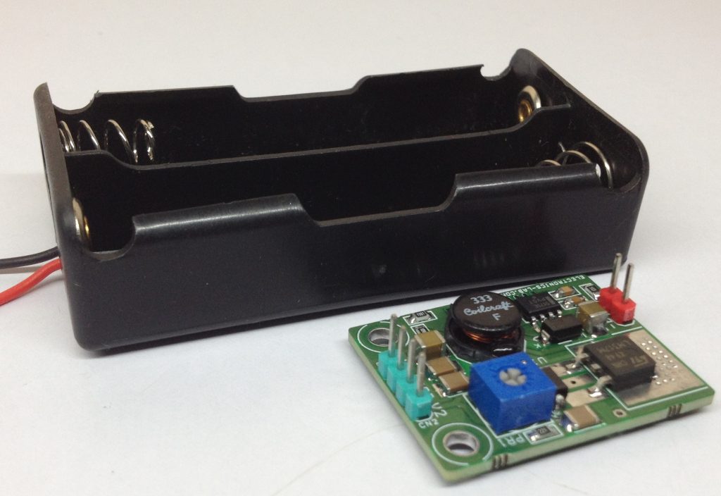
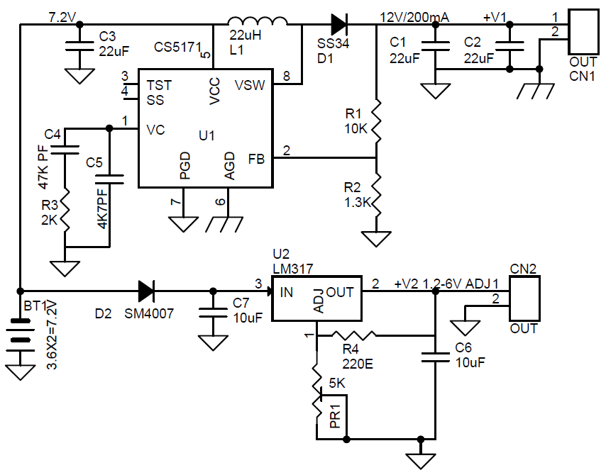
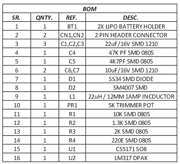
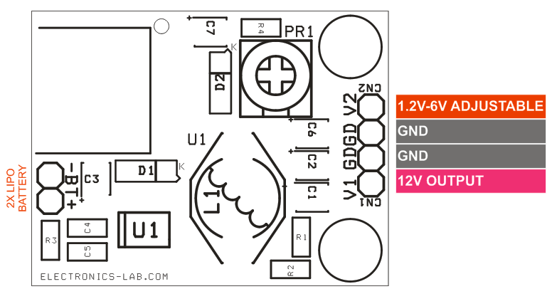
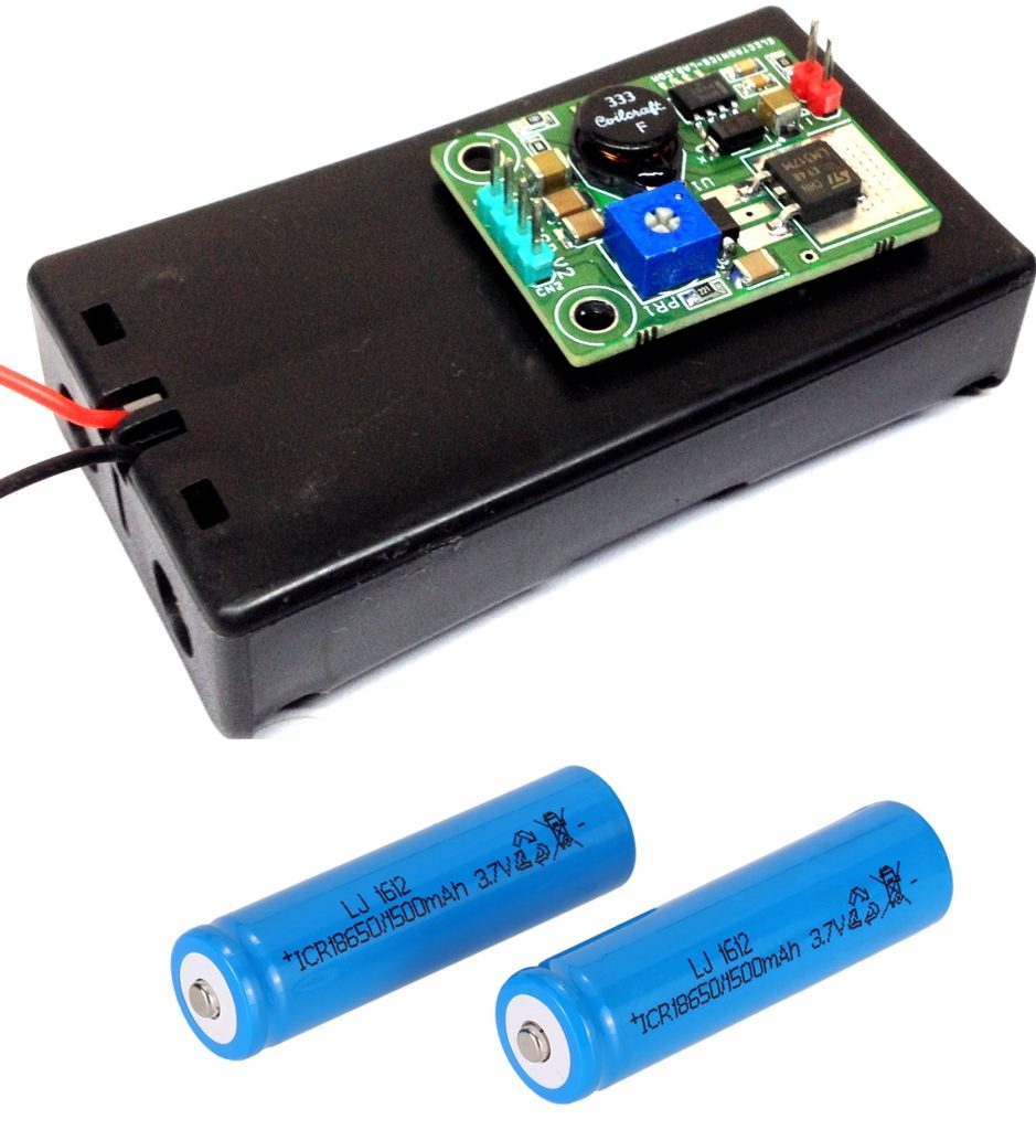
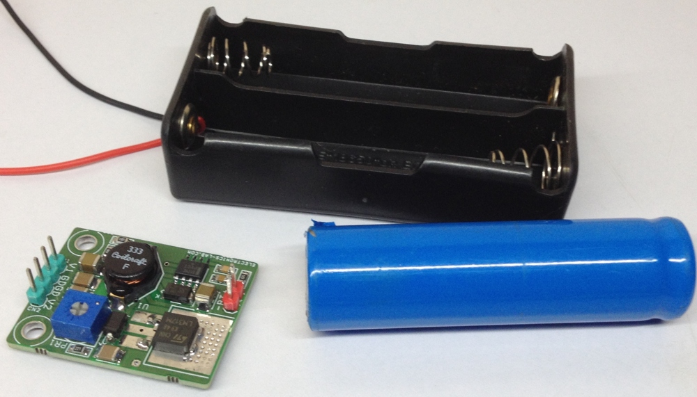
This board provides 12V/200mA DC and 1.2V to 6V/500mA DC Adjustable output with input of 7.4V 2x LiPO batteries. The board is a step up DC-DC Convert based on CS5171 and LM317 adjustable regulator. The Step up DC-DC converter provides 12V DC from 7.4V ( 2x LiPO batteries) and LM317 provides 1.2V to 6V Adjustable Output. The tiny board can directly fitted at the back of the 2 x LiPO CR18650 battery holder using 2xM3 screws. Trimmer potentiometer P1 provided to adjust V2 1.2V to 6V DC. BT1 LiPO Battery , CN1 12V Output, CN2 1.2V 6V Output.
Gyroscopes are present in virtually any modern electronic gadget. They re used in a host of techs, like cell phones, vehicles, drones and wearables. The gyroscopes used presently in our phones will most likely be MEMS-based. Caltech, has gone some extra miles, by successfully developing a new type of gyroscope that is 500 times smaller and 30 times more sensitive than the MEMS version. This research was published in Nature this month.
The conventional MEMS-based gyroscopes functions, by measuring the forces of two identical masses that are oscillating and moving in opposite directions. On the other hand, the optical gyroscope that the Caltech research team developed makes use of lasers rather than MEMS to attain the same result. Even thought the optical gyroscopes are effective in theory, in practice they have been hard to shrink, because the noise-to-signal ratio is inversely proportional to the optical gyroscope’s size.
The new optical gyroscope, is based on Sagnac Effect. This effect was discovered by French physicist Georges Sagnac, and the effect is based on Einstein’s principle of general relativity to identify changes in angular velocity. Majorly, a laser is divided into two beams, and each beam is projected along one side of a disk. As a result of light always traveling at a constant speed, the two beams get to the end of the disk at the same time, as long as the disk is not in motion. If the disk is spinning, the laser beams will get to the end-point out of sync.
The gyroscope measures that difference in synchronization, as the end-point beam has little changes in its properties that can reveal changes in the state of an object, like if you just picked up your phone, or dropped it. The Sagnac Effect however, is often prohibitively sensitive to noise in the signal. Things like small thermal fluctuations, vibrations from moving objects or loud noises can disrupt the beams as they travel.
The smaller the gyroscope is, the more easily it gets disrupted. Infact, the smallest high-performance optical gyroscopes operational today are close to the size of a golf ball. This makes it hard for it to be placed in little gadgets like a watch. To counteract these problems, the Caltech research team came up with the idea of lengthening the path that the laser beams will travel, enabling them to place small disks instead of large ones, while still attaining the same level of accuracy. According to Ali Hajimiri, Bren Professor of Electrical Engineering and Medical Engineering in the Division of Engineering and Applied Science, and the leader of the study, the technique is referred to as “reciprocal sensitivity enhancement.” In this context, “reciprocal” means that it affects both beams of the light inside the gyroscope in the same way.
This technique functions by using two disks instead of one, and then changing the direction that the light travelling from back and forth. This extends the path that the beams are travelling to several thousand rotations instead of one. If the path of the beams is longer, the amount of noise is more even across the two beams, therefore smoothing out defects from outside interference, and this results to an accurate measurement when the beams meet each other at the end. Even though the research has been gain some attention, we should note that it takes a long time for innovations like this to get from the lab to the factories for commercial production. The research has proven that designing optical gyroscopes of this tiny size is possible , but producing the results into a commercial product may take many years to achieve.
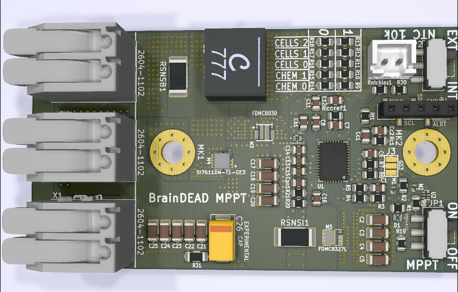
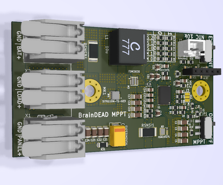
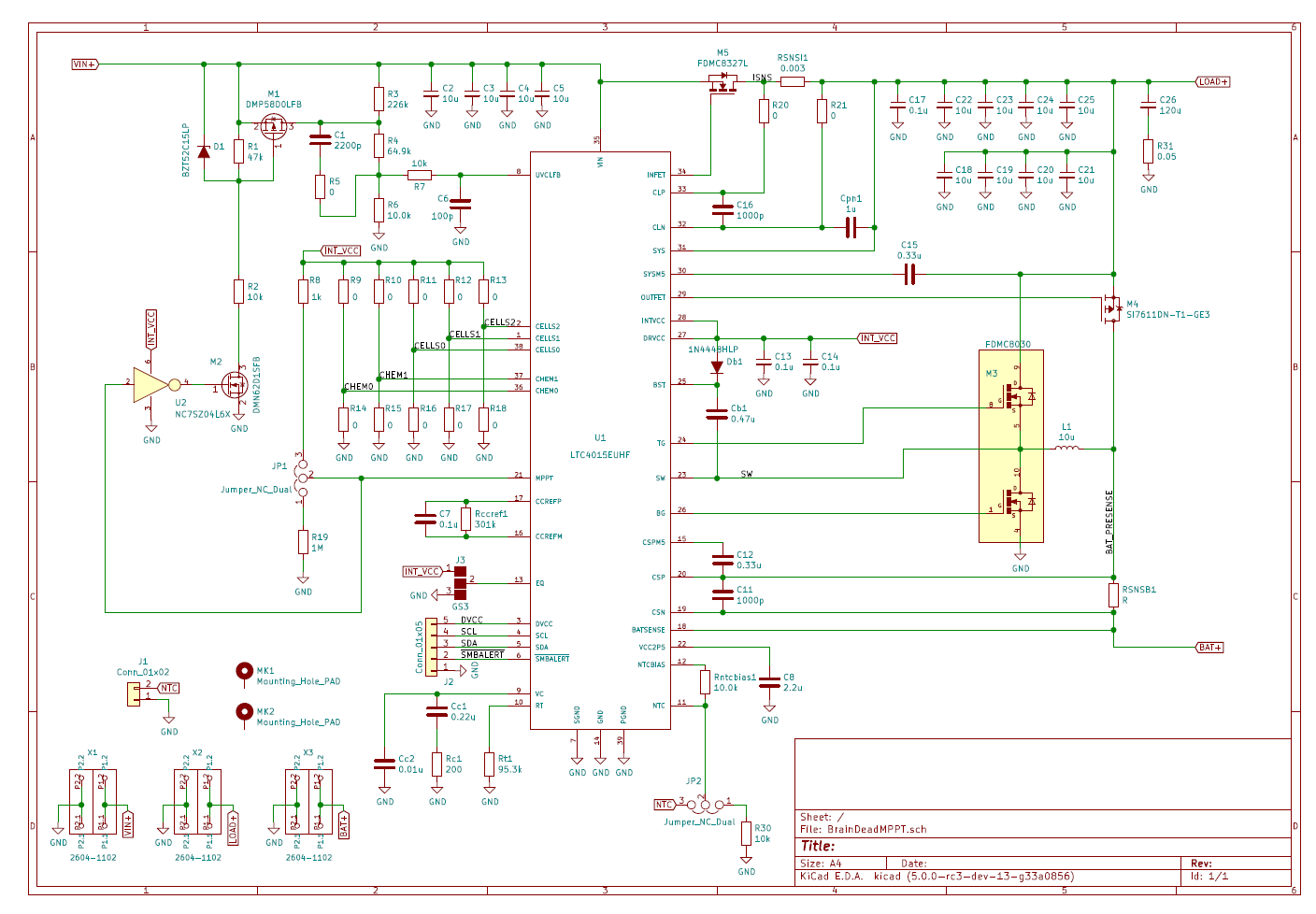
Simple solar charger 35V/8A with automatic MPPT supporting SLA/Li-Ion/LiFePO4 up to 8s. by Adam Lučanský:
PCB DIN-rail mountable MPPT solar charger (software-less), as well as ideal-diode prioritizer (if battery is full, load is powered directly from solar panel without cycling battery). Prototype PCB is in production (as of 20.8.2018) and soon ready for testing. The project is open source and more info & schematics can be found here: https://github.com/lucansky/BrainDeadMPPT
The board is based on LTC4015EUHF (Multichemistry Buck Battery Charger Controller with Digital Telemetry System) from Analog Devices.
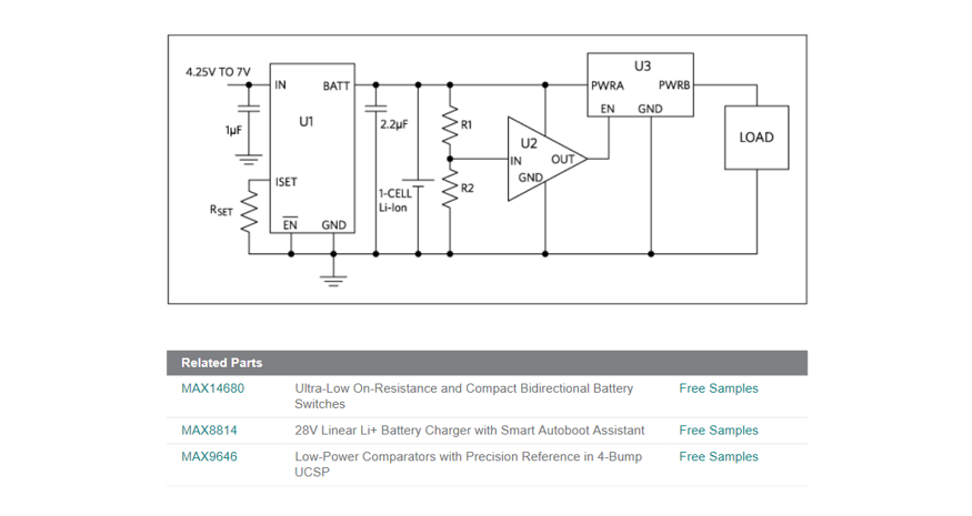
Another app note from Maxim Integrated on small current battery management.The circuit provides a 1-cell Li ion backup battery charger for low-current devices performing resistor limited current sharing.
A simple circuit sometimes needs to charge a 1-cell Lithium-ion (Li+) battery from a USB power source and simultaneously provide backup power for low-current-consumption devices. The circuit in Figure 1 shows such a solution.
MAX9646
Today, most handheld devices use USB as the power source. This design circuit includes a linear, 1-cell charger that accepts a DC power source to charge a 1-cell Li+ battery. The power source provides load current while charging the 1-cell battery. The circuit performs resistor-limited current sharing. The maximum current available is fixed by the setting resistor and that current will primarily drive the load. When the load does not require the full maximum current, the remaining current is available to charge the battery. When the DC source is not available and the cell voltage drops to a user-determined level, a voltage monitor activates an ultra-low-resistance switch to disconnect the cell from the load. This operation avoids a deep discharge of the cell.
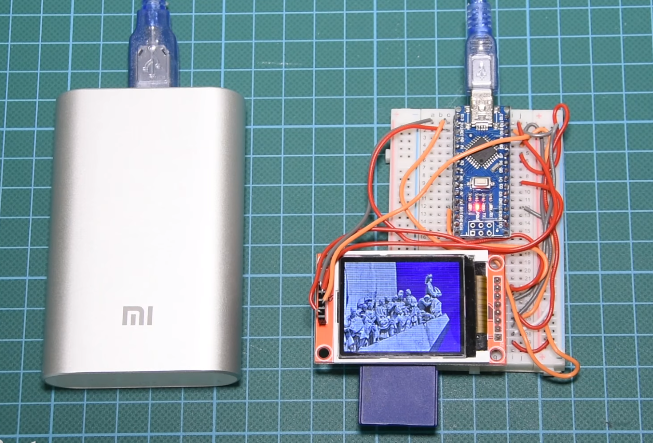
Electronics has transited from a work meant for well-trained engineers to something which is dabbled into by people in other fields especially in Arts and related fields. The introduction of platforms like Arduino (which was created for reasons like this), has been one of the main facilitators of this trend which has produced diverse forms of electronics embedded art pieces, from interactive paintings to animatronic sculptures. For today’s tutorial, we will build our own work of “art” – a digital Photo Frame. Photoframes are used to display pictures or artworks and are made from wood, metal and several synthetic material. They were created to hold just one picture/artwork but with digital photo frames, you could have more than one picture stored on the photo frame, switching between them at desired intervals.
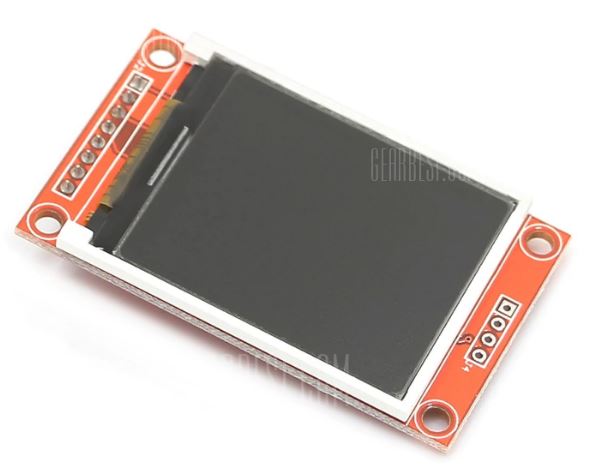
1.8″ TFT Display
Digital Photo frames are usually made up of four main components; a display/screen, a storage device, a microcontroller or microprocessor, and a power supply. For today’s tutorial, we will use the 1.8″ ST7735 based, color TFT as our display and the Arduino nano as the microcontroller. The TFT display is a 1.8″ display with a resolution of 128×160 pixels and can display a wide range of colors ( full 18-bit color, 262,144 shades!). The display uses the SPI protocol for communication and has its own pixel-addressable frame buffer which means it can be used with all kinds of microcontrollers and you only need 4 IO pins. The display module also comes with an SD card slot which we will use as the storage device for this project.
Beside just building the digital photo frame, at the end of this tutorial, you would have also learned how to use the SD card slot on the 1.8″ TFT display module for other projects.
Required Components
The following components are required to build this project;
As usual, the specific components used for this tutorial can be bought via the links attached.
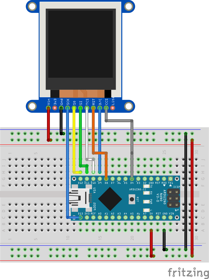
Schematics
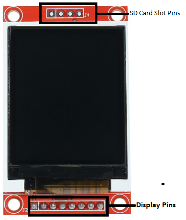
The ST7735 1.8″ TFT display is made up of two set of header pins. The first one at the top consists of 4 pins and are used to interface the SD card slot at the back of the display.
The second set of headers below the screen represent the pins for driving the display itself. However, the SD card slot and the display, both use the SPI protocol for communications with the MCU so they will be connected to the same pins on the Arduino nano. The only difference will be the CS/SS pin as each of them will be connected to a different pin.
Connect the components as shown in the schematics below.
Schematics
For this schematic, we used the Fritzing model of the ST7735 1.8″ TFT display and the arrangement of the pins is slightly different from that of our display. This model has the pins of the SD card slot and the display merged together breaking out only their CS/SS pins.
To make the connections easier to follow, here is a breakdown.
Go over the schematics one more time to be sure everything is as it should be. More on the use of the 1.8″ TFT display was covered in a previous tutorial here.
Preparing the bitmaps
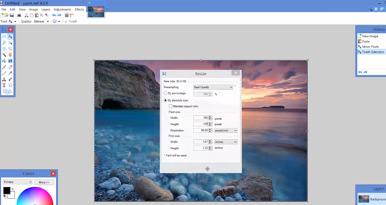
The images that will be displayed on the TFT has to be in a bitmap format, thus before the images are copied to the SD card, we need to convert them to the recognizable bitmap form. To do this, I used the free Paint.net software (for windows) but you can use any other image editing software.
Load the images into the software one by one and use the resize tool to reduce its resolution and size to that (160×128 pixels) of the 1.8″ TFT display.
Editing with paint.net
With this done, save the image on the SDcard with a .bmp extension.
Code
The code for this project is a slightly modified version of the SPI TFT bitmap example shipped with the ST7735 library by Adafruit. Thus the code for this tutorial is heavily reliant on the Adafruit ST7735 and GFX libraries.
To do a quick breakdown of the code, we start by including the libraries that we will use, which include the Adafruit libraries mentioned above, the SPI library and the SD.h library.
//Modified by Nick Koumaris
//info@educ8s.tv
#include <Adafruit_GFX.h>    // Core graphics library
#include <Adafruit_ST7735.h> // Hardware-specific library
#include <SPI.h>
#include <SD.h>
With this done, we declare the pins of the Arduino to which the CS pins of the SD card slot and the TFT are connected and also create an object of the Adafruit ST7735 library with the declared pins passed on as arguments.
#define TFT_CS  10  // Chip select line for TFT display
#define TFT_RST  8  // Reset line for TFT (or see below...)
#define TFT_DC   9  // Data/command line for TFT
#define SD_CS    4  // Chip select line for SD card

Adafruit_ST7735 tft = Adafruit_ST7735(TFT_CS, TFT_DC, TFT_RST);
Next is the void setup() function. We start by initializing serial communication which will be used to debug our code. After this, we initialize the TFT and the SDcard, setting the rotation of the TFT to landscape (represented by 1).
Next is the void loop function. Here we simply invoke the bmpDraw function for each of the images we will like to display, setting a suitable delay time between each of the pictures. The bmpDraw function makes it super easy to display images on the TFT. All we need to do is to provide the name of the .bmp file, starting coordinates and it will use that information to fetch the image from the SD card and display on the screen.
The complete code for the project is shown below. It can also be downloaded from the download section at the end of the tutorial.
//Modified by Nick Koumaris
//info@educ8s.tv
#include <Adafruit_GFX.h> // Core graphics library
#include <Adafruit_ST7735.h> // Hardware-specific library
#include <SPI.h>
#include <SD.h>
#define TFT_CS 10 // Chip select line for TFT display
#define TFT_RST 8 // Reset line for TFT (or see below...)
#define TFT_DC 9 // Data/command line for TFT
#define SD_CS 4 // Chip select line for SD card
Adafruit_ST7735 tft = Adafruit_ST7735(TFT_CS, TFT_DC, TFT_RST);
void setup(void) {
  Serial.begin(9600);

  tft.initR(INITR_BLACKTAB);

  Serial.print("Initializing SD card...");
  if (!SD.begin(SD_CS)) {
    Serial.println("failed!");
    return;
  }
  Serial.println("OK!");

  tft.setRotation(1); // Landscape

}
void loop() {

  bmpDraw("logo.bmp", 0, 0);
  delay(3000);
  bmpDraw("mezapos.bmp",0,0);
  delay(3000);
  bmpDraw("sparti.bmp",0,0);
  delay(3000);
  bmpDraw("mani.bmp",0,0);
  delay(3000);
  bmpDraw("lisbon.bmp",0,0);
  delay(3000);

}
#define BUFFPIXEL 20
void bmpDraw(char *filename, uint8_t x, uint8_t y) {
File bmpFile;
int bmpWidth, bmpHeight; // W+H in pixels
uint8_t bmpDepth; // Bit depth (currently must be 24)
uint32_t bmpImageoffset; // Start of image data in file
uint32_t rowSize; // Not always = bmpWidth; may have padding
uint8_t sdbuffer[3*BUFFPIXEL]; // pixel buffer (R+G+B per pixel)
uint8_t buffidx = sizeof(sdbuffer); // Current position in sdbuffer
boolean goodBmp = false; // Set to true on valid header parse
boolean flip = true; // BMP is stored bottom-to-top
int w, h, row, col;
uint8_t r, g, b;
uint32_t pos = 0, startTime = millis();
if((x >= tft.width()) || (y >= tft.height())) return;
Serial.println();
Serial.print("Loading image '");
Serial.print(filename);
Serial.println('\'');
// Open requested file on SD card
if ((bmpFile = SD.open(filename)) == NULL) {
Serial.print("File not found");
return;
}
// Parse BMP header
if(read16(bmpFile) == 0x4D42) { // BMP signature
Serial.print("File size: "); Serial.println(read32(bmpFile));
(void)read32(bmpFile); // Read & ignore creator bytes
bmpImageoffset = read32(bmpFile); // Start of image data
Serial.print("Image Offset: "); Serial.println(bmpImageoffset, DEC);
// Read DIB header
Serial.print("Header size: "); Serial.println(read32(bmpFile));
bmpWidth = read32(bmpFile);
bmpHeight = read32(bmpFile);
if(read16(bmpFile) == 1) { // # planes -- must be '1'
bmpDepth = read16(bmpFile); // bits per pixel
Serial.print("Bit Depth: "); Serial.println(bmpDepth);
if((bmpDepth == 24) && (read32(bmpFile) == 0)) { // 0 = uncompressed
goodBmp = true; // Supported BMP format -- proceed!
Serial.print("Image size: ");
Serial.print(bmpWidth);
Serial.print('x');
Serial.println(bmpHeight);
// BMP rows are padded (if needed) to 4-byte boundary
rowSize = (bmpWidth * 3 + 3) & ~3;
// If bmpHeight is negative, image is in top-down order.
// This is not canon but has been observed in the wild.
if(bmpHeight < 0) {
bmpHeight = -bmpHeight;
flip = false;
}
// Crop area to be loaded
w = bmpWidth;
h = bmpHeight;
if((x+w-1) >= tft.width()) w = tft.width() - x;
if((y+h-1) >= tft.height()) h = tft.height() - y;
// Set TFT address window to clipped image bounds
tft.setAddrWindow(x, y, x+w-1, y+h-1);
for (row=0; row<h; row++) { // For each scanline...
// Seek to start of scan line. It might seem labor-
// intensive to be doing this on every line, but this
// method covers a lot of gritty details like cropping
// and scanline padding. Also, the seek only takes
// place if the file position actually needs to change
// (avoids a lot of cluster math in SD library).
if(flip) // Bitmap is stored bottom-to-top order (normal BMP)
pos = bmpImageoffset + (bmpHeight - 1 - row) * rowSize;
else // Bitmap is stored top-to-bottom
pos = bmpImageoffset + row * rowSize;
if(bmpFile.position() != pos) { // Need seek?
bmpFile.seek(pos);
buffidx = sizeof(sdbuffer); // Force buffer reload
}
for (col=0; col<w; col++) { // For each pixel...
// Time to read more pixel data?
if (buffidx >= sizeof(sdbuffer)) { // Indeed
bmpFile.read(sdbuffer, sizeof(sdbuffer));
buffidx = 0; // Set index to beginning
}
// Convert pixel from BMP to TFT format, push to display
b = sdbuffer[buffidx++];
g = sdbuffer[buffidx++];
r = sdbuffer[buffidx++];
tft.pushColor(tft.Color565(r,g,b));
} // end pixel
} // end scanline
Serial.print("Loaded in ");
Serial.print(millis() - startTime);
Serial.println(" ms");
} // end goodBmp
}
}
bmpFile.close();
if(!goodBmp) Serial.println("BMP format not recognized.");
}
// These read 16- and 32-bit types from the SD card file.
// BMP data is stored little-endian, Arduino is little-endian too.
// May need to reverse subscript order if porting elsewhere.
uint16_t read16(File f) {
uint16_t result;
((uint8_t *)&result)[0] = f.read(); // LSB
((uint8_t *)&result)[1] = f.read(); // MSB
return result;
}
uint32_t read32(File f) {
uint32_t result;
((uint8_t *)&result)[0] = f.read(); // LSB
((uint8_t *)&result)[1] = f.read();
((uint8_t *)&result)[2] = f.read();
((uint8_t *)&result)[3] = f.read(); // MSB
return result;
}
Demo
Ensure your connections are correct, then upload the code to your Arduino. After a while, you should see the pictures being displayed like a slideshow on the TFT.
Demo
The possibilities attached to the concept shared in this tutorial are limitless. You could make the pictures change based on weather, time of the day or gesture.
That’s it for this tutorial. Do let me know if you have any question about it via the comment section. Feel free to also share ideas on cool modifications and additions that could make the project bigger and more useful.
Till Next time!
The video version of this tutorial can be watched on youtube.
Teledyne LeCroy T3DSO1000 Oscilloscopes are a 2- and 4-channel series of high-speed waveform-capturing devices. The robust T3DSO1000 series can capture up to 400,000wfm/s (in sequence mode), using a 7-inch TFT-LCD to display 256-level, intensity-grading results at 800×480 pixels. This family of oscilloscopes features 100MHz and 200MHz models, a digital intelligent trigger system, security erase mode, pass/fail functions, and USB compatibility. The 4-channel Teledyne LeCroy model is compatible with a number of accessories, including an AWG module, MSO software, and Wi-Fi® software.
Key Features
100 MHz and 200 MHz bandwidths
Sample rates up to 1 GS/s.
Long Memory – up to 7 Mpts/Ch (14 Mpts interleaved)
7” Bright TFT LCD (800 x 480).
Serial Bus Trigger and Decode as standard – I2C, SPI, UART, RS232, CAN, LIN allowing users to debug serial buses directly in the Oscilloscope.
Optional MSO – 16 Digital Channels (4 channel models only) which adds mixed signal debugging to the Oscilloscope.
Advanced Trigger – Edge, Slope, Pulse Width, Window, Runt, Interval, Time Out (Dropout), Pattern.
Waveform Sequence Recorder – record and playback up to 80,000 waveforms. Allows users to replay the changes which have occurred in their waveform history.
Connectivity – USB for mass storage, printing and PC control, plus LAN for fast data transfer.
Record Length Up to 14 Mpts
Using hardware-based Zoom technology the maximum record length of up to 14 Mpts, users are able to over-sample to capture longer time periods at higher resolution and use the zoom feature to see more details within each signal.
Excellent Sampling Rate
Two channel series have one 1 GSa/s ADC, four channel series have two 1 GSa/s ADCs. When all channels are enabled, each channel has a maximum sample rate of 500 MSa/s. When a single channel per ADC is active, it has sample rate of 1 GSa/s.
The T3DSO1000 series employs a new generation of high speed display technology that provides excellent signal clarity, fi delity and performance. The system noise floor is also lower than similar products in the industry. It comes with a minimum vertical input range of 500 uV/div, an innovative digital trigger system with high sensitivity and low jitter, and a waveform capture rate of 400,000 frames/sec (sequence mode). The T3DSO1000 also employs a 256-level intensity grading display function and a color temperature display mode not found in other models in this class. Teledyne Test Tools latest oscilloscope offering supports multiple powerful triggering modes including serial bus triggering. Serial bus decoding for IIC, SPI, UART, CAN, LIN bus types is included. The models also include History waveform recording, and sequential triggering that enable extended waveform recording and analysis.
Another powerful addition is the new 1 million point FFT math function that gives the T3DSO1000 very high frequency resolution when observing signal spectra. The new digital design also includes a hardware co-processor that delivers measurements quickly and accurately without slowing acquisition and front-panel response. The features and performance of Teledyne Test Tools new T3DSO1000 cannot be matched in this price class. The four channel series includes even more functions, including: searching and navigating, on-screen Bode plot, 16 digital channels (Option), an external USB powered 25 MHz AWG module (Option), a USB WIFI adapter (Option), and an embedded application that allows remote control via web browser.
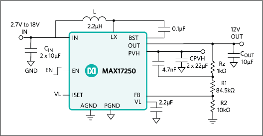
Maxim MAX17250 DC-DC Boost Converter is a high-efficiency, low quiescent current, synchronous boost (step-up) converter with True Shutdown™, programmable input current limit, and short-circuit protection. The MAX17250 has a wide input voltage range of 2.7V to 18V and generates an output voltage of 3V to 18V. The MAX17250 has a maximum on-time of 800ns and implements three modes of operation. The first mode of operation is a soft-start mode at power-up. The second mode of operation is normal operation and utilizes a fixed on-time/minimum off-time Pulse Frequency Modulation (PFM) architecture that uses only 60μA (typ) quiescent current due to the converter switching only when needed. The last mode is True Shutdown, where the output is completely disconnected from the input, and the battery drain is minimized to 0.1µA (typ) shutdown current.
Features
Input Voltage Range 2.7V to 18V
1 or 2 Cell Li-ion Batteries
Output Voltage Range 3V to 18V, > VIN
Integrated Power FETs
Selectable Input Peak Current Limit (ISET)
3.5A, 2.7A, or 1.85A
93% Efficiency
Low Power
0.1µA True Shutdown Current
60µA Quiescent Current
Protection
True Shutdown Prevents Current Flowing Between Input and Output
Soft-Start Inrush Protection
Short-Circuit Protection
Overtemperature Protection
-40°C to +125°C Operation
The Maxim MAX17250 DC-DC boost converter, available from Mouser Electronics, includes a selectable input peak current limit of 3.5 A, 2.7 A, or 1.85 A and operates over an input voltage range of 2.7 V to 18 V with an output voltage range of 3 V to 18 V. The device supports switching frequencies up to 1 MHz and offers short-circuit protection and a maximum on-time of 800 ns in a space-saving 12-bump, 1.72 mm × 1.49 mm package.
The MAX17250 converter implements three modes of operation: The first mode of operation is a soft-start mode at power-up. The second mode of operation is normal operation, which uses a fixed on-time/minimum off-time pulse frequency modulation (PFM) architecture that uses only 60 μA (typical) quiescent current due to the converter switching only when needed. The MAX17250 converter’s True Shutdown™ mode completely disconnects the output from the input, resulting in a current draw of just 0.1 μA, virtually stopping battery drain, providing long battery life, and eliminating the need for external disconnect switches.
Mouser is also stocking the Maxim MAX17250EVKIT#WLP evaluation kit, a fully assembled and tested kit that incorporates the MAX17250 converter and provides resistor-configurable output voltages from 3 V to 18 V.
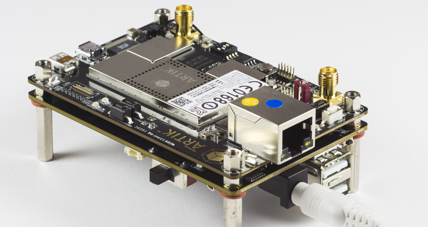
EdgeX Foundry project has launched its first developer kit. The Ubuntu-based kit is designed around an octa-core Samsung Artik 710 Starter Kit paired with a GrovePi+ I/O board. Subsequent kits will have an Artik 530 kit, and ultimately, a Raspberry Pi/GrovePi+ mix. EdgeX Foundry project also announced at the recent IoT Solutions World Congress, where nine new members, including Intel, launched a Smart Building Automation Use Case Community Demo. The demo showcased the platform’s capability to bring together diverse solution components, including series of vendors, connectivity standards, operating systems, and hardware variants. The Artik 710 based EdgeX developer kit is initially available as a community-backed product.
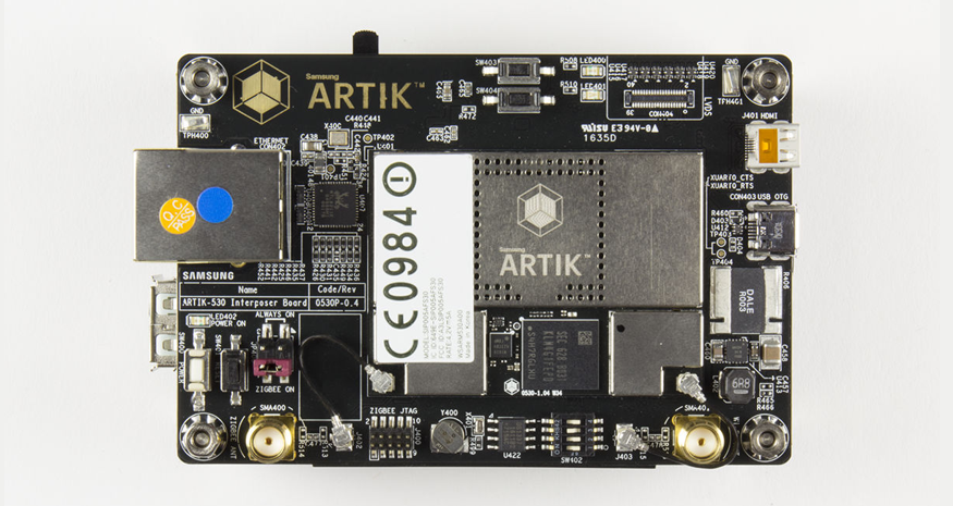
Artik 710 Starter Kit Interposer board
Developers purchase the kit independently from Samsung and download the forthcoming EdgeX Delhi software from the EdgeX depository on GitHub. Unofficial community-based tech support is available via platform like the EdgeX Rocket Chat. This pioneer kit, and also future kits, will soon be available as part of a commercial track that gives professional support. The commercial kits are built primarily for EdgeX members but are now available to everyone.
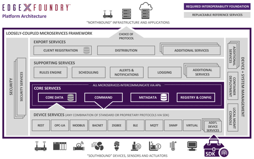
EdgeX Design Architecture
According to the project, commercial selections will include “kits based on supported versions of the EdgeX framework itself (neutral to any plug-in value add), kits based on specific IoT platforms, and microservice plug-ins for value-add such as analytics, data orchestration and security. Samsung’s Artik 710 and Artik 530, which will be the groundwork of an upcoming EdgeX kit, changed their BSPs from Fedora to Ubuntu in October 2017.
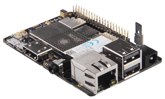
The Artik 710 module has a 1.4GHz, octa-core, -A53 SoC with a Mali T400 GPU, and the Artik 530 has a 1.2GHz, quad-core, -A9 SoC. Both have hardware security properties. The 49 x 36mm modules incorporates 1GB DDR3 RAM, 4GB eMMC flash, and an Ethernet PHY. They also offer dual-band 802.11a/b/g/n (WiFi 4), Bluetooth 4.2, and Zigbee/Thread (802.15.4). The Artik 710 Developer Kit is a twin board set. The Interposer Board has the Artik 710 plus Gigabit Ethernet, micro-HDMI, and micro-USB OTG ports. LVDS interface and antenna connectors are available.
The Platform Board is placed under the Interposer board and offers a USB 2.0 host port, SD slot, audio jack, JTAG, 5V DC input, and MIPI-CSI and -DSI connections. The EdgeX version of the Artik 710 kit also has the optional Artik Interface II Board, which connects the bundled Seeed GrovePi+ I/O board. The GrovePi+ Starter Kit offers a a number of Grove sensors and LEDs, a backlit LCD, buzzer, relay, and button. The GrovePi+ Starter Kit is also a part of Samsung’s GrovePi+ Starter Kit for Eagleye 530 board, which will the foundation of the future Artik 530 kit. Unlike the Artik 710 kit, the Artik 530 fitted Eagleye 530 is a single board with a Raspberry Pi like layout, design , and 40-pin GPIO interface.
Eagleye 530 board
The Eagleye 530 is also fitted with GbE and HDMI ports, 2x USB 2.0 ports, and micro-USB OTG and power ports. Also, an SD slot, audio jack, and MIPI-CSI camera interface are available. Unlike the Artik 710 kit, the Eagleye 530 does not need the Interface II Board to hook up the bundled GrovePi+ board. The GrovePi+ board will be available in a future EdgeX kit that runs on the GrovePi+ Starter Kit for Raspberry Pi.
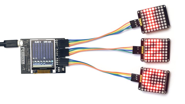
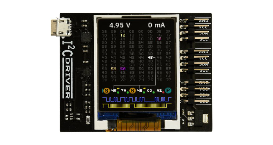
I²CDriver is an easy-to-use, open source tool for controlling I²C devices. It works with Windows, Mac, and Linux, and has a built-in color screen that shows a live “dashboard” of all the I²C activity. It uses a standard FTDI USB serial chip to talk to the PC, so no special drivers need to be installed. The board includes a separate 3.3 V supply with voltage and current monitoring.
I²C is Everywhere
It’s in every phone, in your embedded electronics, in every microcontroller, Raspberry Pi, and PC motherboard. It’s a mature technology – still going strong after 36 years. Because it’s everywhere, I²C is used by everyone from novices to embedded designers. But the common element of everyone’s I²C experience is struggle. Instead of being easy, I²C very often feels really difficult. Because there are so many ways for I²C to go wrong, things rarely “just work” and instead involve some painful debugging.
I²CDriver Makes I²C Much More Friendly
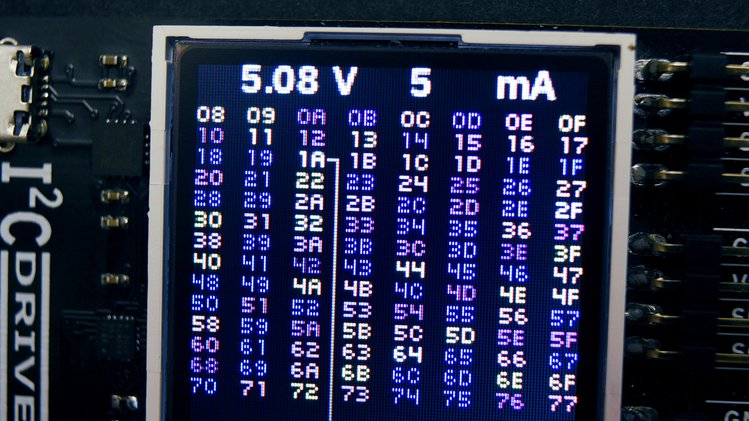
The heat map shows all 7-bit I²C addresses
While other I²C tools might offer a couple of LEDs, I²CDriver has a clear logic-analyzer display of the signal lines plus a graphical decoding of the I²C traffic.
In addition, it continuously displays an address map of all attached I²C devices, so as you connect a device, it lights up on the map. You’ll never have to ask “is this thing even switched on?” again.
The current and voltage monitoring let you catch electrical problems early. The included color-coded wires make hookup a cinch; no pinout diagram is required. It includes a separate 3.3 V supply for your devices, a high-side current meter, and programmable pullup resistors for both I²C lines.
There are three I²C ports, so you can hook up multiple devices without any fuss.
Do More With I²CDriver
I²CDriver driving three 8×8 LED modules
By controlling I²C hardware using the PC tools you’re most comfortable with, you can get devices doing what you want in a fraction of the development time. Calibrating devices like accelerometers, magnetometers, and gyroscopes is much simpler and faster when done directly on the PC through I²CDriver.
Features
Open hardware: the design, firmware and all tools are under BSD license
Live display: shows you exactly what it’s doing all the time
Fast transfer: sustained I²C transfers at 400 and 100 kHz
USB power monitoring: USB line voltage monitor to detect supply problems, to 0.01 V
Target power monitoring: target device high-side current measurement, to 5 mA
I²C pullups: programmable I²C pullup resistors, with automatic tuning
Three I²C ports: three identical I²C ports, each with power and I²C signals
Jumpers: color coded jumpers included in each pledge level
3.3 output: output levels are 3.3 V, all are 5 V tolerant
Supports all I²C features: 7- and 10-bit I²C addressing, clock stretching, bus arbitration
Sturdy componentry: uses an FTDI USB serial adapter, and Silicon Labs automotive-grade EFM8 controller
Usage reporting: reports uptime, temperature, and running CRC of all traffic
Flexible control: GUI, command-line, C/C++, and Python 2/3 host software provided for Windows, Mac, and Linux
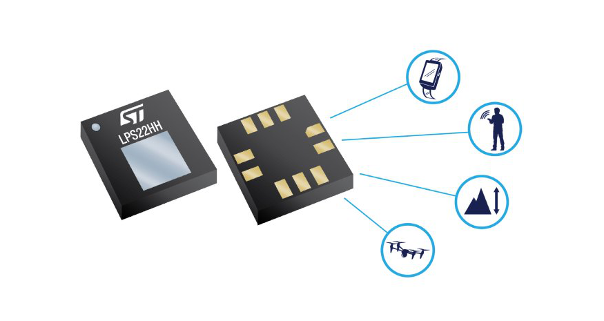
The LPS22HH is an ultra-compact piezoresistive absolute pressure sensor which functions as a digital output barometer. The device comprises a sensing element and an IC interface which communicates through I²C, MIPI I3CSM or SPI from the sensing element to the application.
The sensing element, which detects absolute pressure, consists of a suspended membrane manufactured using a dedicated process developed by ST.
The LPS22HH is available in a full-mold, holed LGA package (HLGA). It is guaranteed to operate over a temperature range extending from -40 °C to +85 °C. The package is holed to allow external pressure to reach the sensing element.