Artificial Intelligence has been the talks of most markets and development in the last few years. It is widely believed that the products and solutions of tomorrow will have one form of artificial intelligence built into them. Companies and Organisation are spending millions of dollars in R&D in the areas of AI in health, AI in transportation, AI in Finance and several others. What about the everyday makers? For us that don’t yet have access to the millions of dollars, how can we start innovating with AI especially AI in the Edge? Development platform like the Lichee Dan is making this possible.
Lichee Dan combines two beautiful worlds together: Open source and Artificial Intelligence into one single platform. Lichee Dan which is also officially named the Sipeed M1 series is an excellent open source AI development kit made by the team behind the LicheePi boards. They aim to promote AI-related development and education.
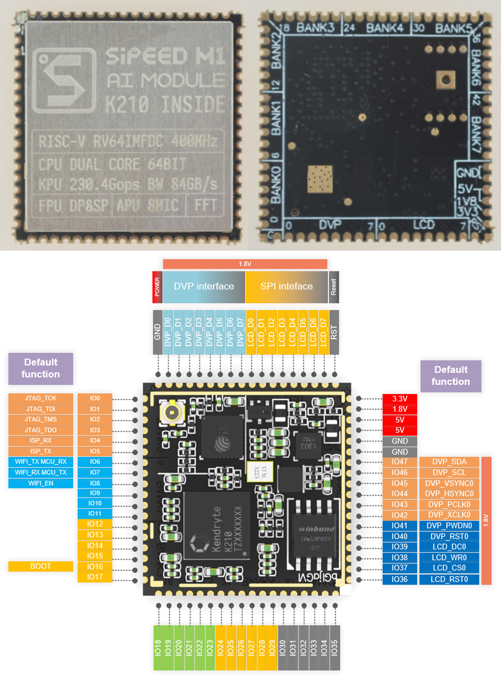
Sipeed M1 Module
Unlike the conventional C or C++ seen in most hardware boards, the Sipeed M1 integrates Micropython to make development pretty smooth and straightforward. At the heart of the Sipeed M1 platform is the AI chip K210 by Kendryte, a dual-core RISC-V with an FPU. It serves as the core unit and dual-core processing with independent FPU, 64-bit CPU and 8M in-built SRAM. With a 400Mhz adjustable nominal frequency it supports multiplication, division and square root operation.
Below are the Sipeed M1 module specs:
SoC – Kendryte K210 dual core 64-bit RISC-V processor @ 400 MHz with KPU CNN hardware accelerator, APU audio hardware accelerator, 6 MB general purpose SRAM, 2MB AI SRAM memory, and AXI ROM to load user program from SPI flash
Package – 72-pin (25.4 x 25.4mm)
The Lichee Dan/ Sipeed M1 has the following features:
Neural Network Processor (KPU)
Audio processor (APU)
Fast Fourier Transform Accelerator (FFT Accelerator)
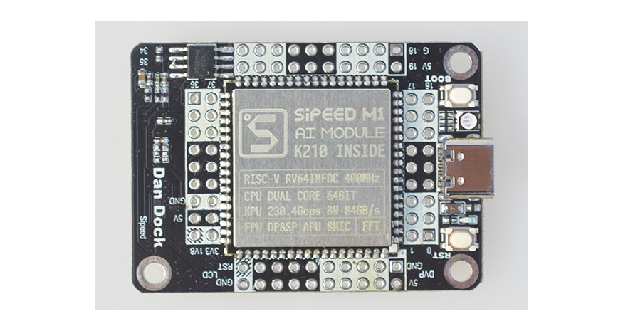
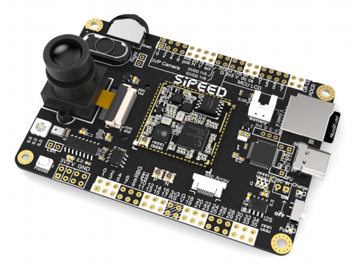
The 72pin board might be pretty difficult to use on its own, but thanks to the Sipeed MAIX development board called the Dan Dock, you can have access to all the functionality and some extras as well. In the AI processing, AI Chip (K210) can perform operations such as convolution, batch normalization, activation, and pooling. At the same time, the pre-processing of voice direction scanning and voice data output can also be performed. It offers [email protected], 400MHz, and when you overclock to 800MHz, it offers 0.5TOPS. This means you can do object recognition with a rate of 60fps@VGA resolution.
Sipeed M1 Development Board
The module is pretty powerful, and the video below shows an illustration of the device used for real-time face detection. One of the best thing about the module is not only the low cost and the small size but also the power consumption.
The main features of the development board include:
Storage – micro SD slot
Display I/F – An FPC24P socket for 8-bit MCU LCD
Camera I/F- An FPC24P socket for DVP camera
Audio – Power amplifier IC for use with speakers, built-in microphone
USB – USB Type-C interface
Connectivity – Optional WiFi
I/Os
On-board high-speed DAC
Access to all 72-pin full pin lead-out, freely mappable
The development board Dan Dock is currently being crowdfunded on IndieGoGo with different price offers ranging from $5 to about $15 for each unit. The Sipeed MI module is also available for purchase on Taobao (in Chinese) and yoycart for about $12.45. More information about the product is available on the campaign page and the module documentation.
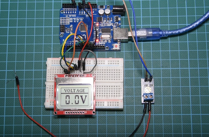
Voltage is one of the fundamental values when dealing with electronics. It determines the amount and direction of current flow and represents the potential (electric charge) difference between two points, thus it is somewhat impossible to build or troubleshoot electronics circuits without being faced with the need to measure the voltage at one point or the other. The instrumentation device used for measuring the voltage is called a Voltmeter and for today’s tutorial, I will be demonstrating how you can build your own DIY version using an Arduino.
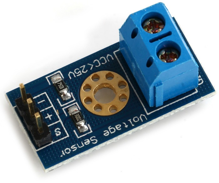
B25 Voltage Sensor module
Since voltage could either be direct (DC) or alternating (AC), one can either measure the AC or the DC voltage. For today’s tutorial, to keep things simple, we will focus on the measurement of voltage in a DC-based setup using the B25 voltage sensor module.
The B25 voltage sensor is a cheap, 25v maximum input, analog sensor which uses the voltage divider principle to give a value on output, corresponding to the input voltage. The sensor uses a linear conversion system such as that the value at the output is directly proportional to the input, thus, when working with the Arduino, it is important to ensure that a voltage greater than 25V is not applied at the module’s input as this will drive the voltage at the output beyond 5v which may lead to your Arduino board being damaged. While the sensor is probably cheap enough, you could build your own version using two resistors, set up as a voltage divider.
Arduino Voltmeter with LCD display
While several AC measuring principles exist, we can use a DC voltmeter to measure AC voltage but this should only be done after rectification and regulation of the input to a value tolerable by the DC side of the system. Correlation and mapping can then be done to indicate the value of AC voltage represented by the DC voltage (e.g 5VDC could represent 220VAC).
A major application of this project could be to keep track of the battery life of your project.
Required Components
The following components are required to build this project;
As usual, the exact one used for this tutorial can be bought via the link attached to them.
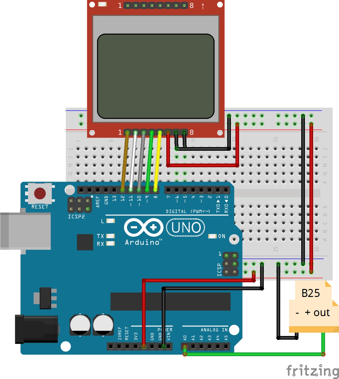
Schematics
The schematics for this project is quite easy. Connect the components as shown below.
Schematics
As mentioned earlier, the B25 voltage sensor is an analog device as such, its output is connected to the analog pin of the Arduino. To make the schematics easier to follow there is a breakdown of how the devices are connected, pin to pin.
We have done quite a number of tutorials which involves the use of the Nokia 5110 LCD. You may want to check one of them (especially this one) to better understand its connection and use.
With the connections done, we are now ready to write the code.
Code
The code for this project is quite simple. All we need to do is to read the voltage of the voltage sensor, convert it to the corrresponding voltage and display the value on the Nokia 5110 LCD Display. To display the information in a user-friendly manner, we will create a user interface for the LCD display which is attached together with the code in the zip file under the download section. We covered how to develop a user interface in one of the previous tutorials. To easily write the code to interface with the Nokia 5110 LCD display, we used the LCD5110_Graph library which can be downloaded from the link attached.
To do a run-through of the code; we will start by including the header files of the libraries that will be used, after which we create an object of the LCD library, specifying the pins of the Arduino to which the LCD is connected.
//written by Nick Koumaris
//info@educ8s.tv
#include <LCD5110_Graph.h> // THE LIBRARY I AM USING IS THIS:  http://www.rinkydinkelectronics.com/library.php?id=47

LCD5110 lcd(8,9,10,12,11);
Next, we specify the variable name to hold the font style, the UI, and the splash screen graphics after which we declare the analog pin of the microcontroller to which, the signal pin of the voltage sensor is connected.
extern unsigned char BigNumbers[];
extern uint8_t ui[];
extern uint8_t startScreen[];

float voltage = 0.0;
int sensorPin = A0;
We then declare some of the other variables that will be used.
Next is the void setup function. Here, we initialize the serial port and LCD after which, we issue the command to display the splash screen and set the font style to be used to display text on the LCD.
Next is the void loop function. The task under this section is simple; call the read voltage function to obtain the voltage value and display the value on the serial monitor and the LCD. The value is converted to a string for easy display on the LCD and a delay of 1000ms is applied after it has been displayed, just so it stays long enough on the screen to be seen before the Arduino code loops.
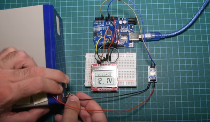
Upload the code to your Arduino and test with any battery or DC source you have. Ensure you don’t exceed the maximum input voltage of 25V so you don’t damage the Arduino. The LCD display should display the voltage level as shown in the picture below.
Demo
That’s it for this tutorial guys. Kindly drop any question or comments under the comments section. Will try to reply to as many as possible.
Till next time!
The video version of this tutorial can be found on youtube.
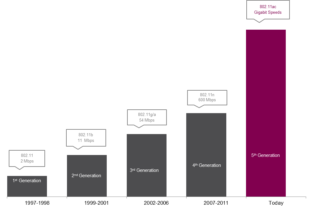
WiFi 5 also known as 802.11ac has been around for a while now, but few boards have adopted it. The WiFi 5 might easily be confused with the general WiFi (802.11 b/g/n). The WiFi standard 802.11ac is capable of 1300 megabits per second (Mbps) which is the equivalent of 162.5 megabytes per second (MBps), this is 3x faster than the typical 450Mbps speed attributed to 802.11n. So obviously WiFi 5 promise so much in the development of next-generation IoT and connected applications.
photo: wi-fi.org
WiFi and Bluetooth connectivity almost always come together and having both WiFi and Bluetooth always gives a system more robustness. The Expressif ESP32WiSoC is one of such solutions that offers engineers Wifi 802.11 b/g/n and Bluetooth 4.2 but what about the early movers that wants to try the best of both technologies, i.e., WiFi 5 and Bluetooth 5? Well, Espressif Systems doesn’t yet offer anything in that domain, instead you might have to consider the less known UniSoC UWP5661 Arm Cortex-M4 WiSoC chip.
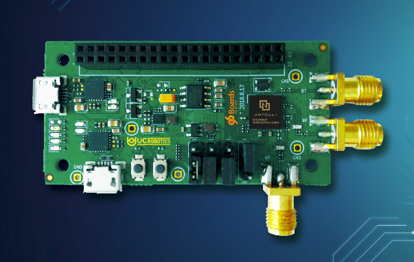
IVY5661 96Boards IoT Edition board
Little information is currently available about the WiSoC chip, but the SoC is what will power the soon to be launch IVY5661 96Boards IoT Edition board that features 802.11ac (WiFi 5) and Bluetooth 5 by UcRobotics. The new IoT hardware platform is believed to run the Zephyr OS, and no build documentation is currently available as nothing is available on the product page here.
Below are some the IVY5661 board specifications:
SoC – UniSoC UWP5661 dual core Arm Cortex-M4 microcontroller @ 416 MHz manufactured with 28nm process
Storage – 32Mbit NOR flash
Connectivity (built-in SoC) – Dual-band 802.11ac 2×2 MIMO WiFi, Bluetooth 5
USB – 2x Micro USB
Expansion Interface – 96boards LS (Low Speed) connector with UART, I2C, SPI, I2S, GPIO
Misc – 4x user LED, 2x reset and user button
Power Supply – 5V via Micro USB port
Dimensions – 60 x 30 mm (96Boards IoT edition form factor)
Well, that’s all we know about the UniSoC UWP5661 Arm Cortex-M4 WiSoC chip and the IVY5661 96Boards IoT Edition board pending to be launched. For the meantime, we will keep working around the ESP32 WiSoC while appreciating the amazing community making all these possible.
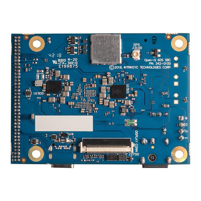
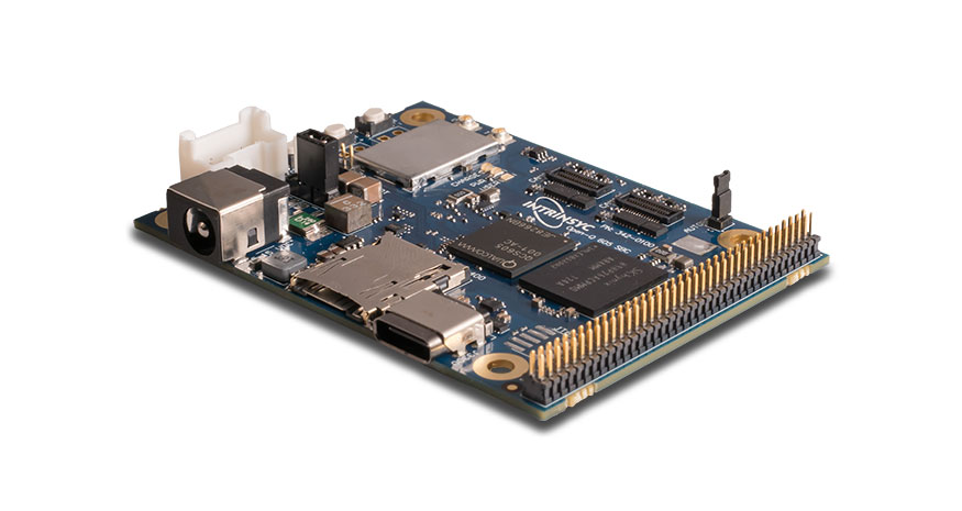
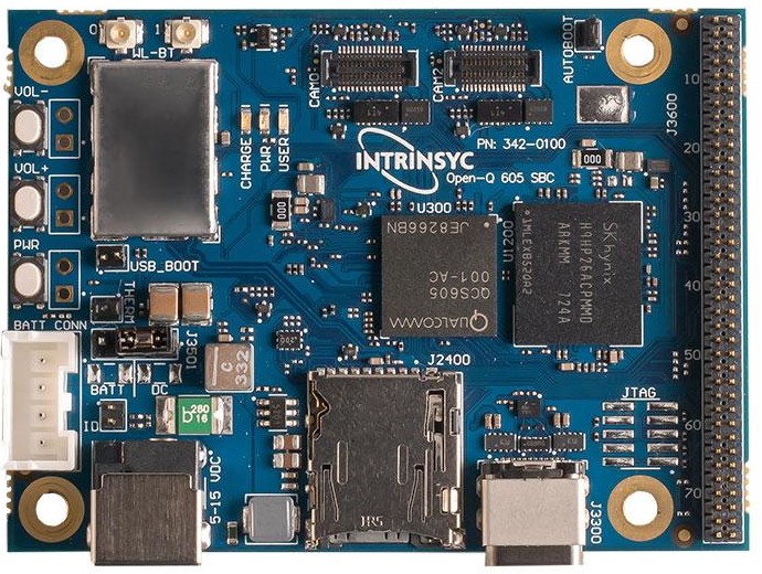
Qualcomm announced back in April its QCS605 SoC, calling it “the first 10nm FinFET fabricated SoC, built for the Internet of Things.” The octa-core Arm SoC is available in an Intrinsyc Open-Q 605 SBC with full development kit, including a 12V power supply which is available for pre-order at $429. The product will ship in early December. The QCS605 has a Qualcomm Vision Intelligence Platform, a set of mostly software components that include the Qualcomm Neural Processing SDK and camera processing software and also the company’s 802.11ac WiFi, Bluetooth connectivity and security technologies.
Open q-605 front
The QCS605 can run on Linux or Android, but Open-Q 605 board supports only Android 8.1. Intrinsyc also recently released an Open-Q 624A Development Kit modeled on a new Open-Q 624A SOM. The QCS605 SoC is equipped with 8x Kryo 300 CPU cores, two of which are 2.5GHz “gold” cores that are equal to Cortex-A75. The other six are 1.7GHz “silver” cores like the Cortex-A55 — Arm’s more powerful follow-on to Cortex-A53. The QCS605 also incorporates an Adreno 615 GPU, a Hexagon 685 DSP with Hexagon vector extensions (“HVX”), and a Spectra 270 ISP that supports dual 16-megapixel image sensors. Qualcomm also has a QCS603 model on sale, which is identical except that it has only 2x of the 1.7GHz “Silver” cores instead of six.
Qualcomm markets the QCS605 as part of a Vision Intelligence Platform, which is a combination of software and hardware starting with a Qualcomm AI Engine built around the Qualcomm Snapdragon Neural Processing Engine (NPE) software framework. The NPE enables analysis, optimization, and debugging tools for developing with Tensorflow, Caffe, and Caffe2 frameworks. The AI Engine also includes the Open Neural Network Exchange interchange format, the Android Neural Networks API, and the Qualcomm Hexagon Neural Network library, which enables the porting of trained networks.
The Vision Intelligence Platform available on the QCS605 offers up to 2.1 TOPS (trillion operations per second) of compute performance for deep neural network inferences, according to Qualcomm. The platform also supports up to 4K @ 60fps resolution or 5.7K at 30fps and supports multiple simultaneous video streams at a lower resolution. The board also features a “staggered” HDR to prevent ghost effects in the high-dynamic-range video.
Also, advanced electronic image stabilization, de-warp, de-noise, chromatic aberration correction, and motion compensated temporal filters in hardware are available. Apart from the Snapdragon 600 based Open-Q 600, the Open-Q 605 is the only Open-Q development board that Intrinsyc tags as an SBC. Many of Open-Q’s kits are compute modules or sandwich-style carrier board starter kits based on Intrinsyc modules fitted with Snapdragon SoCs, such as the recent, Snapdragon 670 based Open-Q 670 HDK. The 68 x 50mm Open-Q 605 will ship with an eMCP package with 4GB LPDDR4x RAM and 32GB eMMC flash, and additional storage is available through a microSD slot.
Open q-605 back
The QCS605 depends on the 802.11ac (WiFi 5) and Bluetooth 5.x radios for networking. A Qualcomm GNSS receiver for location and 3x U.FL connectors is also available. The QCS605 is equipped with a real-world coastline port USB Type-C that supports DisplayPort 1.4 with 4K@30fps support. If you want to use the Type-C port for USB or charging a user-supplied Li-Ion battery, you can resort to an HD-ready MIPI DSI interface with touch support. 2x MIPI-CSI is also available for dual cameras, as well as 2x analog audio. The Open-Q 605 has a 76-pin expansion header for other interfaces, including an I2S/SLIMBus digital audio interface. The board runs on a 5-15V DC input and offers an extended -25 to 60°C operating range.
Specifications listed for the Open-Q 605 SBC include:
Processor — Qualcomm QCS605 with Vision Intelligence Platform (2x up to 2.5GHz and 6x up to 1.7GHz Krait 300 cores); Adreno 615 GPU; Hexagon 685 DSP; Spectra 270 ISP; Qualcomm AI Engine and other VIP components
Memory/storage — 4GB LPDDR4X and 32GB eMMC flash in combo eMCP package; microSD slot.
Wireless: 802.11b/g/n/ac 2×2 dual-band WiFi (Qualcomm WCN3990) with planned FCC/IC/CE certification, Bluetooth 5.x, Qualcomm GNSS (SDR660G) receiver with Qualcomm Location Suite Gen9 VT, U.FL antenna connectors for WiFi, BT, GNSS
Media I/O: DisplayPort 1.4 via USB Type-C up to 4K@30 with USB data concurrency (USB and power), MIPI DSI (4-lane) with I2C touch interface on flex cable connector for up to 1080p30, 2x MIPI-CSI (4-lane) with micro-camera module connectors, 2x analog mic I/Ps, speaker O/P, headset I/O, I2S/SLIMBus digital audio interface with 2x DMIC ports (via 76-pin expansion header)
Expansion — 76-pin header (multiple SPI, I2C, UART, GPIO, and sensor I/O; digital and analog audio I/O, LED flash O/P, haptic O/P, power output rails
Other features — 3x LEDs; 4x mounting holes; optional dev kit with quick start guide, docs, SW updates
Operating temperature — -25 to 60°C
Power — 5-15V DC jack and support for user-supplied Li-Ion battery with USB Type-C charging; PM670 + PM670L PMIC; 12V supply with dev kit
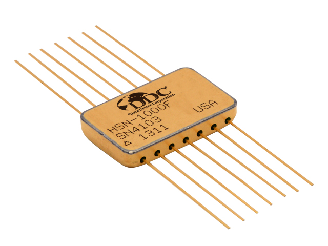
DDC’s HSN-1000 radiation-hardened Hybrid Nuclear Event Detector (NED) senses ionizing radiation pulses generated by a nuclear event, such as the detonation of a nuclear weapon, and rapidly switches its output from the normal high state to a low state with a propagation delay time of less than 20ns. The active low Nuclear Event Detection signal (NED) is used to initiate a wide variety of circumvention functions, thus preventing upset and burnout of electronic components. The NED output is also used to initiate both hardware and software recovery. This high-speed, 14-pin hybrid detector is used in electronic systems as a general-purpose circumvention device to protect memory, stop data processing, and drive power supply switches as well as signal clamps.
The HSN-1000 is guaranteed to operate through three critical environments: ionizing dose rate [1012 rad(Si)/s], gamma total dose [106 rad(Si)], and neutron fluence [5 x 10¹³ n/cm2]. In addition, the device is designed to function throughout the transient neutron pulse. The hybrid’s discrete design ensures a controlled response in these radiation environments as well as immunity to latchup. Each HSN-1000’s detection level and functionality are tested in an ionizing dose rate environment. A certificate is provided with each serialized hybrid, reporting the radiation test results and guaranteeing its performance. The device is also lot qualified in the total dose and neutron environments to ensure performance.
The detection threshold of the HSN-1000 is adjustable within the range of 2 x 10⁵ rad(Si)/s to 2 x 10⁷ rad(Si)/s. This detection level can be preset by DDC or adjusted by the user. Less than a 30% variation in detection threshold can be expected over the entire operating temperature range.
Features:
Detects ionizing radiation pulses
100% tested/certified detection threshold level
Adjustable circumvention period
100% testable with built-in test
Detection threshold adjustability
Single +5V operation
Radiation hardness guaranteed
Compliant to MIL-PRF-38534 Class H
Flat pack (F) or DIP (L) packages
Radiation Hardness Characteristics:
Dose Rate (operate-through): 1 x 10¹² rad(Si)/sec
Total Dose: 1 x 10⁶ rad(Si)
Neutron Fluence: 5 x 10¹³ n/cm2
Approximate Detection Range: 2 x 10⁵ – 2 x 10⁷ rad(Si)/sec
Atmosic Technologies Inc. (Saratoga, CA) has launched the M2 and M3 Bluetooth 5.0 transceiver chips, claiming them to be the lowest power Bluetooth wireless chips available.
Atmosic took a wireless agnostic approach to determine the most power-efficient foundation for its first IoT connectivity solutions. To radically reduce power consumption, Atmosic has developed three key technologies: Lowest Power Radio, On-demand Wake-up, and Controlled Energy Harvesting. With Lowest Power Radio and On-demand Wake-Up, Atmosic enables 10X to 100X lower power, reducing power utilization to a level that Controlled Energy Harvesting is a viable power source. With the addition of Controlled Energy Harvesting, the solution can deliver forever battery life or battery-free operation.
Lowest Power Radio is based on the team’s extensive wireless and low-power experience, which has enabled Atmosic to achieve radical power performance improvements while maintaining full standards compliance.
To create On-demand Wake-Up, Atmosic has implemented two levels of listening: one provides the lowest level of “radio consciousness” to perceive incoming transmissions; the other is a deep sleeper, waking only when alerted to incoming transmissions by the “radio consciousness” portion. On-demand Wake-Up requires coordination with the host, which would send a special pattern to wake-up, causing Atmosic ICs within range to wake-up. While this may cause some radios to wake-up unnecessarily, the number of wakeups will still be vastly lower than a typical beacon’s 86,400 wake-ups per day based on a time interval of one second.
Instead of relying on ambient energy harvesting, which is inherently unpredictable, Atmosic’s Controlled Energy Harvesting technology is based on a known energy source that can be controlled to guarantee robust, deterministic functionality while minimizing the system dependence on battery power. The technology can work in the 2.4GHz or 900MHz bands. As an example, a computer could be used to emit a deterministic RF energy source for a mouse or wireless keyboard in close proximity.
For its first products, Atmosic recently unveiled the industry’s lowest power standards-compliant wireless Bluetooth 5 platforms, according to the company, comprising the M2 and M3 series. Bluetooth 5 provides performance increases over legacy Bluetooth by 4X the range (now comparable to Wi-Fi), 2X the speed, and 8X the bandwidth.
The Atmosic M2 Series Bluetooth 5 SoC features Lowest Power Radio delivering 5X to 10X lower power; the addition of On-demand Wake-up reduces power by 10X to 100X. The Atmosic M3 Series Bluetooth 5 SoC adds Controlled Energy Harvesting to provide forever battery life or eliminate the need for battery power. Packaging options for the M2 and M3 Series include flash and non-flash, 5×5 QFN, and 6×6 DRQFN packages. The ICs incorporate an Arm Cortex-M0 processor and assorted peripherals to form a complete solution.
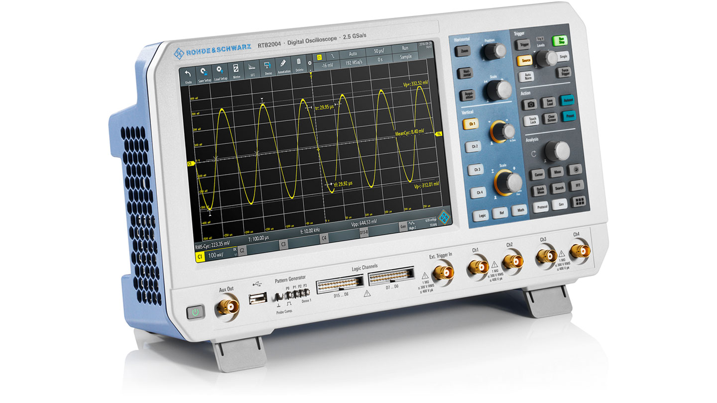
Power of ten (10-bit ADC, 10 Msample memory and 10.1″ touchscreen) combined with smart operating concepts make the R&S®RTB2000 oscilloscopes the perfect tool for university laboratories, for troubleshooting embedded designs during development and for production and service departments.
RTB2000 has the largest display (10.1″) with the highest resolution of 1280 × 800 pixel in its class, a capacitive touchscreen to quickly navigate in pop-up menus and a touch function to easily adjust scaling, to zoom in or to move a waveform – it works just like your smartphone.
The 10-bit A/D converter provides up to a fourfold improvement when compared to the conventional 8-bit A/D converters. You get sharper waveforms with more signal details.
10 Msample memory depth is available for each active channel. When interleaved, even 20 Msample are available. That is 10 times more than comparable oscilloscopes offer. This captures longer signal sequences for more analysis results.
Features:
Bandwidth: 70 MHz to 300 MHz
Sample rate: up to 2.5 Gsample/s
Memory depth: up to 20 Msample
ADC resolution: 10 bit
Display: 10.1″ capacitive touchscreen
The R&S® RTB2000 gives users more than just an oscilloscope. It also includes logic analyzer, protocol analyzer, waveform and pattern generator and digital voltmeter.
Dedicated operating modes for frequency analysis, mask, tests and long data acquisitions are also integrated. Debugging all kinds of electronic systems is easy and efficient.
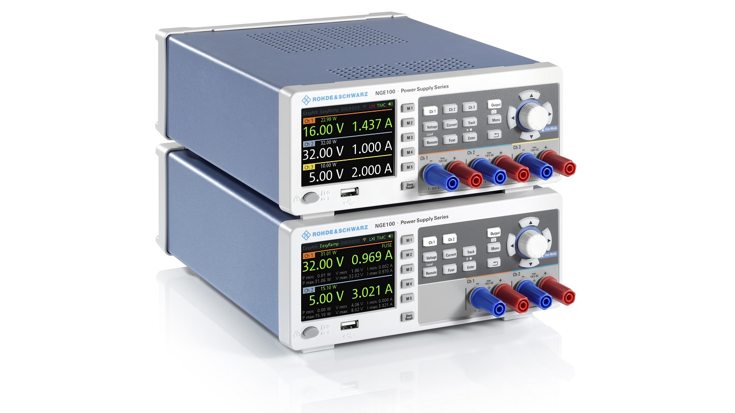
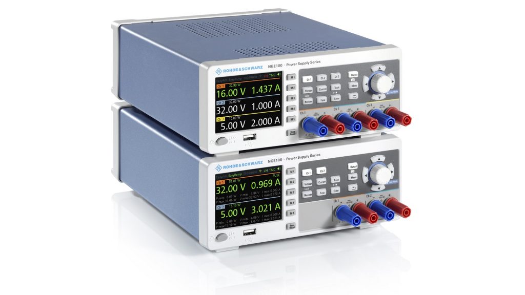
The new power supply series consists of the R&S NGE102B with two channels and the R&S NGE103B with three channels. They are suitable for various applications in education and production as well as in R&D labs. With these new features, Rohde & Schwarz is addressing the educational sector in particular.
The power supplies’ new colour-coding of the channels simplifies operation. Thanks to regulated fans, the R&S NGE100B series is also particularly quiet. In addition, the inputs and outputs are now equipped with safety binding posts, eliminating the need for adapters. The R&S NGE100B series power supplies can be remotely controlled via the integrated USB interface and optionally via LAN or WLAN, which is especially useful for education.
Galvanically isolated channels
In addition, the R&S NGE100B series features some functions that are exceptional in this price class: all channels are galvanically isolated, floating and electrically identical. This allows each channel to be operated as an independent power supply. Higher output voltages and currents can be achieved by combining the channels in serial or in parallel.
Adjustable maximum current, voltage and power
The easy-to-use safety functions protect the device under test and the power supply, even in complex setups. This allows maximum voltages and currents to be set and shutdown scenarios to be defined.
Basic equipment for educational applications
Combined with the R&S RTB2000 oscilloscope, the R&S FPC1500 spectrum analyser and the R&S HM8012 digital multimeter, the R&S NGE100B power supplies are ideal for universities and R&D laboratories. These instruments are all part of the company’s Value Instruments portfolio, which offers high-performance entry-level T&M equipment at competitive prices.
The power supplies are available now from Rohde & Schwarz and selected sales partners, with prices starting at EUR 650. The new series is replacing the R&S NGE100 series. Rohde & Schwarz will continue to provide software updates, service and maintenance for the R&S NGE100 predecessor series.
Murata has announced a new 3-axis inclination sensor with a tilt angle output and digital SPI interface. The high performance SCL3300 series of devices will be used in a variety of demanding applications including levelling, tilt sensing, machine control and structural health monitoring.
Based on Murata’s proven 3D-MEMS sensing technology, the SCL3300-D01 is a 3-axis (XYZ) inclinometer with four user selectable measurement modes which can be used to optimise the sensor’s performance for different applications and their requirements. The highly integrated device includes a mixed signal ASIC for signal processing along with a flexible digital interface that removes the need for an external ADC, reducing size, power use and design complexity. The SCL3300-D01 features sophisticated tilt angle conversion inside the sensor which enables simple and robust application software and reduces required engineering work. Robust sensor design and advanced self-diagnostics features ensure that the output from the device can be relied on at all times.
The SCL3300-D01 inclinometer provides a ±90° tilt angle output which simplifies measuring software and device usage. The device operates from -40 °C to +125 °C with a typical offset temperature drift less than ±10 mg across the entire operating temperature range. The ultra-low noise density is as low as 0.001°/√Hz for high measurement resolution.
The SCL3300-D01 operates from a single 3.3 V supply and is ideal for battery-powered operation in remote locations, including IoT-based applications, due to a typical sleep mode current draw of just 3 μA.
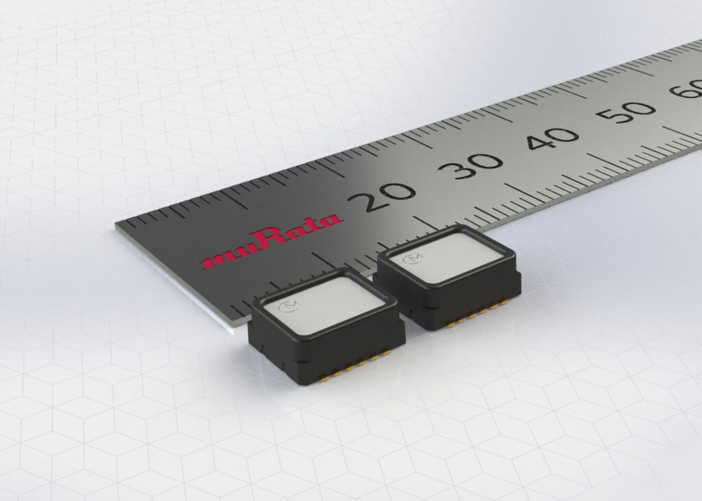
Housed in a 12-pin pre-moulded plastic housing (8.6 mm x 7.6 mm x 3.3 mm LxWxH) that guarantees reliable operation over the product’s lifetime, the inclinometer is suitable for SMD mounting and is compatible with the RoHS and ELV directives.
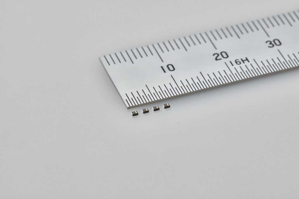
Over 60% Smaller than Conventional Products, Contributing to the Development of Smaller Wearable Devices. [via]
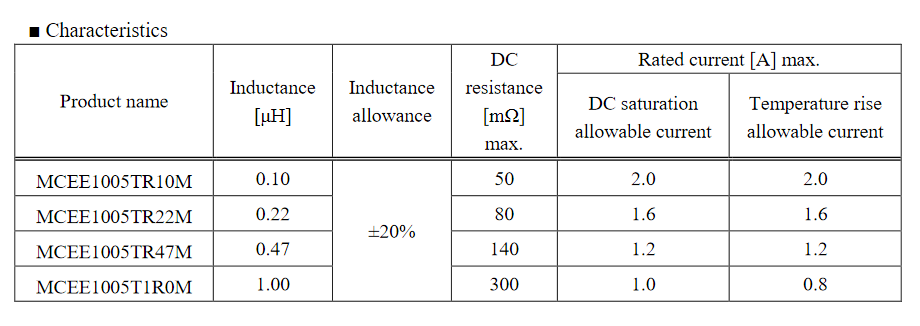
The expansion of the line-up of the metal multilayer chip power inductor MCOIL MC series, from TAIYO YUDEN, which uses a metallic magnetic material, as well as the commercialisation of the tiny metal power inductor MCEE1005 (1.0×0.5×0.55mm, maximum height), has been announced.
This power inductor is used as a power choke coil in power supply circuits for wearable devices, smartphones, and IoT devices. By sophisticating material and multilayer techniques, TAIYO YUDEN has successfully commercialised the 1005-size metal power inductor, achieving a volume that is reportedly over 60% smaller than its conventional product, MCFK1608 (1.6×0.8×0.6mm), and will contribute to developing smaller and thinner mobile devices such as wearable devices.
Production of the product started at the subsidiary company, WAKAYAMA TAIYO YUDEN in Japan’s Wakayama prefecture from September 2018 at a production rate of 10 million units per month.
Today’s market for smartwatches, wristband-type wearable devices, and IoT devices like sensor network devices requires not only reduced size and thickness but also highly efficient power supply circuits for longer operating time. While smartphones are getting thinner, they use higher-speed processors for higher performance and multi-core processors for higher efficiency.
Since high-speed multi-core processors, which are driven by lower voltage and larger current, use appropriate cores in accordance with processor load, each core is equipped with a dedicated power supply circuit, which requires small and thin power inductors with a large current capacity.
To address this market need, TAIYO YUDEN has commercialised its metal multilayer chip power inductor MCOIL MC series, which uses a metallic magnetic material with high DC bias characteristics and has the advantage of being small and thin.