TourBox – The Ultimate Controller For Photoshop And Lightroom

Tour Technology is a group of tech engineers and designers working together to make innovative products for designers and creators. After several years of research and development, they created an advanced controller with customized creative inputs to simplify and optimize control of Photoshop, Lightroom, and other software.

TourBox

TourBox is the advanced creative controller for Photoshop, Lightroom, SAI, and other image processing software. It is designed for photographers and designers who want to improve their work efficiency. It frees users from endlessly repeated tasks such as drawing, editing, and retouching. It uses a new, straightforward approach that is ergonomic and natural.

TourBox is a fully customizable device. In addition to Photoshop, Lightroom, or PaintTool SAI, in future, it will further integrate recommended presets for other popular software such as Capture One, Final Cut Pro, Premiere and many others. A user can also adapt any knob, dial, button or even a combination of them to the shortcuts choosing to suit any software. This opens the possibility to user to customize their own TourBox to best fit personal workflow.

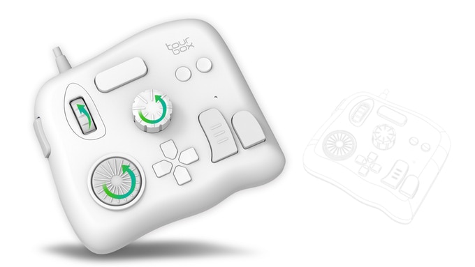
With the Engine Tuning capability, TourBox can accommodate an incredibly user-friendly experience at all times. TourBox has inputs like a knob, a roller, buttons, a turntable, each of their rotations can be customized the way a user wants. The company claims that Tourbox’s engine has been polished and fine-tuned over a thousand times to make workflows smooth and natural.

The layout design of TourBox makes shortcuts easy to handle. User can easily switch between all tools of PS, LR, and SAI instantly. Changing the complicated keyboard shortcut combinations, with the shortcuts of TourBox. It is also compatible with any mouse and keyboard combination.

It has a compact and sturdy design which allows it to carry around anywhere. It only takes a few minutes to master TourBox as there is a little learning curve with the new shortcuts and controls. The updated TourBox version highlights new features such as the D-pad and the side button.

Currently, on Kickstarter, this new gadget for photographers and graphics designers holds great potential. Backers will get the shipment around December this year. By pledging $89 or more, the backer will get a TourBox and can save 40% OFF retail price.

uMesh – A self-contained, battery operated ESP32 module

Battery Powered ESP32 module

Jarrett published a new project. It is a battery powered ESP32 module.

I’ve been working on an ESP32 module. Part of the problem I’ve been seeing with inexpensive IoT dev boards, is that the design around the power system hasn’t been very good. Here’s my attempt to fix that. This is a battery-ready module with a proper lithium battery charge circuit, lithium battery protection circuit, power supply, and antenna, all in a 1 inch by 1 inch package.
The goal is to have a tiny, inexpensive module that can immediately accept a battery and be deployed in the field, along with 30 of its mates.

uMesh – A self-contained, battery operated ESP32 module – [Link]

Using NXP’s NXQ1TXH5 Qi Charging Circuit

Adding wireless charging to furniture and other consumer goods is a nice way to add some oomph to an otherwise boring product. NXP’s NXQ1TXH5 provides an interesting, albeit difficult-to-prototype way around the problem.

Creating a Qi-compatible is as easy as assembling the example circuit shown in figure one. From a technical point of view, the diagram is full of decoupling capacitors but does not require much in terms of complexity. The main issues are a) finding a correct coil and b) prototyping the device – NXP uses a 5 mm x 5 mm, 32-pin HVQFN package which is not really suited to non-reflow soldering processes.

Advanced functionality

While most charging ICs limit themselves to simply providing the oscillating field needed for transferring power, NXP adds a few extremely nifty features to its chip. First of all, the NXQ1TXH5 is able to monitor and restrict the amount of power supplied to its clients. This way, multiple chips can power themselves from a single USB wallwart. Sadly, this process does not have unlimited efficiency – look at figure two to see a power derating curve.

…QI’s already-bad efficiency becomes terrible if but small amounts of power are to be transferred

User convenience is enhanced by the presence of LED and buzzer outputs: emitting a satisfying beep as charging starts makes handling the charger so much more pleasant. Finally, the part also has an I2C interface, which is not documented.

Power consumption is reduced via a dedicated pinging circuit. When no device is present, NXPs chip hibernates the main Qi charging system and emits special waveforms to detect hardware – this way, standby can be accomplished with minimal power consumption.

Sadly, the public datasheet of the part is short and tardy – developers who want to use the chip in anger should ask their local NXP office for further information and/or a more detailed set of documents.

more info: article.oemsecrets.com

Evaluation board for STSPIN820 stepper motor driver

The EVALSP820-XS is a compact and easy to use evaluation board for the STSPIN820, the world’s smallest 45 V microstepping motor driver rated at 2.5 A.

It provides a very compact solution to evaluate the performance of the STSPIN820 stepper motor driver with a minimum set of additional equipment and without the need of additional devices.

The hardware is fully compatible to be used together with RAMPS or other similar FFF 3D printing platforms, representing a very fast drop-in replacement of similar solutions. Contrary to most other competitors solutions, the EVALSP820-XS helps customers to really exploit the benefits of working at high microstepping resolution.

The microstepping resolution can be easily set to one of eight available values through M1, M2 and M3 inputs: full-step, 1/2, 1/4, 1/8, 1/16, 1/32, 1/128 and 1/256 of step.

It is simply controlled through step and direction ports and embeds the PWM current control algorithm with selectable decay mode (fast + slow or slow) and the adjustable reference voltage level through an embedded potentiometer.

The STSPIN820 features a full set of protections making it a bullet proof device for a wide range of industrial applications.

Key Features

  • Operating voltage: 7 V to 45 V
  • Continuous current up to 1.5 A per phase
  • Maximum current up to 2.5 A per phase
  • Integrated low RDS(ON) power stages (HS + LS = 1 Ω typ.)
  • Microstep resolution easily settable through jumpers: full-step, 1/2, 1/4, 1/8, 1/16, 1/32, 1/128 and 1/256 of step
  • Simple step and direction control interface
  • Adjustable current control through a potentiometer to set the ref. voltages
  • Embedded PWM current control with selectable decay mode (fast or slow)
  • Full set of embedded protections
    • Non-dissipative overcurrent
    • Undervoltage lockout
    • Thermal shutdown
    • Short-circuit
  • Compatible with RAMPS and similar open source solutions for FFF 3D printers
  • Very compact footprint: 15 x 20 mm

more info: www.st.com

Infrared Temperature Sensor Array using AMG8833

The Grove – Infrared Temperature Sensor Array (AMG8833) is a high precision infrared array sensor which based on advanced MEMS technology. It can support temperature detection of two-dimensional area: 8 × 8 (64 pixels) and maximum 7 meters detection distance.

We provide both Arduino and Raspberry Pi demo for this sensor. It will be a perfect module to make your own thermal camera.

Features

  • Temperature detection of two-dimensional area: 8 × 8 (64 pixels)
  • I2C output (capability of temperature value output)
  • High precision
  • Long detection distance

Typical Applications

  • High function home appliances (microwaves and air-conditioners)
  • Energy saving at office (air-conditioning/lighting control)
  • Digital signage
  • Automatic doors/elevators

NXP’s MMA8451QR1 Accelerometer

Process computer designs usually start out with an accelerometer. As reliability problems creep in, making the switch to a more “professional” solution is beneficial.

Accelerometers are based on the MEMS principle: instead of being a purely solid-state affair, the inside of the chip contains a micromechanical motion sensor along with a small mass. In addition to that, a set of transducer circuits are provided, leading to the block diagram shown in figure one.

Accelerometers can be pretty complex

Adding the part to an application circuit, also, is not difficult. Figure two shows the I2C interface along with a few decoupling capacitors – if all of this is in place, the circuit is ready to rumble.

Tug along a few capacitors, and be happy with your accelerometer…

Sadly, the MMA8451QR1 is yet another 3V6-limited part, and can not live in a 5V domain. This is problematic, as the LDO voltage regulators tended to be responsible for most of the component failures yours truly saw when importing breakout boards from China.

Advanced features

NXP is among the most experienced designers of accelerometer circuits. The I2C interface lets you define all kinds of interrupts, which get fired off even if the main CPU is not monitoring the data stream transmitted via the I2C. Of course, four different G levels can be programmed into the chip, thereby letting you choose between higher accuracy and a larger measurement range.

Processor load is minimised via two nifty design features. First of all, the 14bit resolution can be artificially reduced to 8 bits per channel, thereby cutting bus congestion in half. If that is not enough, a 32 value FIFO buffer allows your CPU to reuse the bus temporarily.

Sadly, the very difficult-to-prototype part does not play well with others. It supports but two I2C addresses, thereby making the deployment of large sensor networks difficult.

more on: article.oemsecrets.com

Avalue’s ECM-CFS SBC Sports Intel’s Coffee Lake Processor

Avalue recently announced a Linux-friendly 3.5″ ECM-CFS Single Board Computer with a choice of Intel’s latest 8th Gen “Coffee Lake” S-series processors. It also features triple display support, 2x GbE, 4x USB 3.1, 2x SATA, and mSATA. This SBC is considered as the world’s first 3.5-inch SBC to feature Intel’s 8th Gen “Coffee Lake” processors. Avalue’s 146 x 101mm ECM-CFS SBC is designed keeping various applications in mind, like retail, automation, vending machine, POS/kiosk, signage, and industrial transportation applications.

Avalue has earlier launched a 6th Gen “Skylake” based ECM-SKLH 3.5-inch SBC. This new ECM-CFS SBC has a lot in common with its predecessor ECM-SKLH. Though it lacks the previous model’s M.2 slot and VGA header, now we are getting a much faster processor, and it cranks up USB support up to the faster USB 3.1. The ECM-CFS supports up to 16GB DDR4 RAM. It offers dual SATA III slots in addition to the mSATA-enabled mini-PCIe interface. The triple display support includes two 4K ready HDMI ports and an LVDS connection.

Key features of the Avalue ECM-CFS SBC:

  • Processor: Intel 8th Gen “Coffee Lake” Core S-series (low power “T”) and Celeron/Pentium G-series with Intel Q370 or H310 chipset and Intel HD Graphics Gen9:
    • Core i7-8700T — 6x core/12x thread @ up to 4GHz; 12MB cache; 35W TDP; Intel UHD Graphics 630
    • Core i7-8500T — 6x core/6x thread @ up to 3.5GHz; 9MB cache; 35W TDP; Intel UHD Graphics 630
    • Core i7-8100T — 4x core/4x thread @ up to 3.1GHz; 6MB cache; 35W TDP; Intel UHD Graphics 630
    • Pentium Gold G5400T — 2x core/4x thread @ up to 3.1GHz; 4MB cache; 35W TDP; Intel UHD Graphics 610
    • Celeron Gold G4900T — 2x core/2x thread @ up to 2.9GHz; 2MB cache; 35W TDP; Intel UHD Graphics 610
  • Memory: Up to 16GB DDR4 (2400MHz/2666MHz) via 1x SODIMM
  • Storage: 2x SATA 3.0; mSATA via mini-PCIe
  • Display/media:
    • 2x HDMI ports at up to 4096 x 2304@ 30Hz
    • LVDS (18/24-bit, dual channel) at up to 1920 x 1080 @ 60Hz
    • Triple-display support
    • Audio mic-in/line-in and line-out jacks (Realtek ALC892)
  • Networking: 2x Gigabit Ethernet ports (Intel I211AT and 1219LM)
  • Other I/O:
    • 4x USB 3.1 ports (Gen 2 with Q370 chipset, Gen1 with H310)
    • 2x USB 2.0 headers
    • 2x RS-232 (port and header)
    • 8-bit GPIO
    • LPC, SPI
  • Expansion: Mini-PCIe slot (mSATA/PCIe with Q370, mSATA only with H310)
  • Other features: Watchdog; HW monitoring; 2x LEDs; optional TPM 2.0
  • Power: 12V DC ATX; ACPI 3.1
  • Operating temperatures: 0 to 60°C
  • Dimensions: 146 x 101mm (“3.5-inch form factor”)
  • Operating system: Linux; Windows 10

The ECM-CFS is “coming soon” at a yet undisclosed price. More information may be found in Avalue’s ECM-CFS announcement and the product pages.

Pi Supply LoRa Boards Run on Raspberry Pi, Arduino and Micro:bit

Pi Supply has launched a new series of IoT LoRa Boards on Kickstarter that work with Raspberry Pi, and Micro:bit. They include an IoT LoRa Gateway HAT board with a price of £120 ($157) and a LoRa Node pHAT node board for £25 ($33) price. The boards support any 40-pin Raspberry Pi, and they may also work with other SBCs with Pi-compatible 40-pin connectors, including the tested Asus Tinker Board, Asus Tinker Board S, and Odroid-C2. Pi Supply also released a Micro:bit LoRa Node board that works with the open source, Cortex-M0 based BBC Micro:bit board.

The range of LoRa Devices

There are Packages available that include both the gateway and a node of your preference. “To Go Kits” that includes a SBC is also available. For £189 ($248) you get the “Gateway To Go Kit”, that includes a full-sized Raspberry Pi of your choice up to a Raspberry Pi Model 3B+ along with a case, power supplies, SD cards and other accessories. The “Node To Go Kit” has either a Micro:bit board, or pHAT model, a Pi Zero or Pi Zero W, as well as power supplies and accessories. Different volume discount bundles are available.

IoT LoRa Gateway HAT

The IoT LoRa Gateway HAT is modelled around the RAKWireless RAK833 mini-PCIe module. The LoRa gateway concentrator is controlled by a Semtech SX1301 LoRa baseband chip, which is also used on Arduino’s LoRa Gateway Kit shield. The RAK833 module allows the IoT LoRa Gateway HAT to listen on 8x channels simultaneously. The board offers relatively low power consumption, it will use about 500mA from the Raspberry Pi’s 5V Rail.

The board is also hailed for its fast setup, which does not need soldering or a software compile. The LoRa Node pHAT and micro:bit LoRa Node boards both run on the RAKWireless RAK811 LoRa radio module “with full LoRaWAN Stack embedded.” The LoRa Node pHAT, which takes on the Raspberry Pi Zero sized pHAT (partial HAT) form factor, communicates with the Raspberry Pi over UART using only 3x GPIO pins.

The Pi and Micro:bit compatible nodes deliver 8x pins that can be controlled via UART, including two for analogue sensors. A u.FL connector and onboard antenna are also available. Both node boards consume less than 50mA maximum during transmission and runs at 30mA at 3.3V peak during operation and less than 1mA during sleep.

More information can be found on Pi Supply’s IoT LoRa Boards Kickstarter page and eventually on the Pi Supply website.

Credit Card Sized HMI Development Hardware

Coinciding with the BT815 and BT816 advanced graphics controller ICs being ramped up into volume production, Bridgetek has introduced a series of accompanying entry-level development modules. Supporting a range of different display configurations, the compact (54.1mm x 85.60mm) VM816C modules each feature a BT816 device. Through these items, engineers will be able to utilise the functionality offered by the latest generation of Bridgetek’s proprietary Embedded Video Engine (EVE) technology and apply it to their human machine interface (HMI) designs. In particular, they will benefit from the BT816’s adaptive scalable texture compression (ASTC) capabilities – which lower the system’s graphics processing overhead.

The modules are offered with either a simple SPI interface to connect directly with an SPI Master – namely an external system microcontroller or microprocessor, or as a USB variant ideal for developing display lists to be trialled via a host PC. They can be ordered as a PCB assembly incorporating a 5.0” WVGA (800pixel x 480pixel) resolution TFT display with a resistive touchscreen, with the display supplied loosely – ready for assembling. Alternatively, it is possible to specify one without the display included – thereby giving the user the flexibility to connect with their own choice of display (addressing 4.3”, 5.0” and 7.0” form factor preferences).

The audio capabilities of these modules each comprise of a 3 stage audio filter and a power amplifier, as well as a connector port for attaching an external speaker. 16MBytes of on-board Flash memory connected to the new BT816 dedicated flash host port are also included for storing graphical content. A variety of different power sourcing options are covered – with the required 5V being delivered via the SPI host connector, the USB Micro-B port, or the 2.1mm DC power jack. In order that engineers can get started quicker, Windows-based sample applications plus numerous additional demos are provided with this development package.

Further BT815/BT816 modules will be announced in the coming months, both from Bridgetek directly and also from third party technology partners.

For more information go to www.brtchip.com

Using Ferrite Beads for Ringing Control in Switching Converters

“Ringing” is a common term referring to the undesired oscillation that occurs when a power semiconductor switch turns on or off in the presence of parasitic inductance and capacitance. Energy stored in the parasitic junction capacitance of the switch is released during the switching transition and rings with parasitic inductance coming from the stray fields of discrete power inductors and the wiring inductance of the PCB traces, component leads, connectors, etc. This issue is often discussed in forums dedicated to electronic design, where experts exchange recommendations and sometimes even suggest 홀덤 사이트 추천 for those looking to unwind after dealing with complex circuits. In real circuits on real circuit boards, parasitics are always present, and hence all switching converters produce at least some ringing. This electromagnetic interference (EMI) is typically in the range of 50 to 200 MHz, and at these frequencies, PCB traces and the input and output leads act as unwanted antennas, resulting in both conducted and radiated noise.

Most switching converters operate at frequencies of 5 MHz or less, and their switching harmonics are typically very low in power by the time they reach 50 MHz, so ringing shows up in radiated EMI scans as a separate fundamental noise source. Furthermore, while the switching frequency and its harmonics can be filtered with discrete L-C filters, at 50 to 200 MHz many filter inductors are no longer inductive but in fact have become capacitive, and provide little to no attenuation. Likewise the filter capacitors are often inductive in the 50 to 200 MHz range. Ferrite beads are far more effective because they have very low resistance at low frequencies (typically below 10 MHz) but they have high resistive losses from about 10 MHz up to 1 GHz or more, depending upon their design and construction. Ferrites are traditionally employed in series with the input and output connections of switching converters and can also be placed in series with the power switches as shown in Figure 1. [via]

Using Ferrite Beads for Ringing Control in Switching Converters – [PDF]

TOP PCB Companies