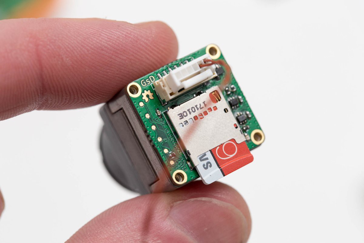
Simple FPGA based PCB to capture thermal images from a FLIR Boson camera on to a microSD. The project’s sources are available on Github. by Greg Davill
A small PCB designed to attach to the backside of the FLIR Boson Thermal Camera. The PCB facilitates configuration of the camera along with capturing data to an SD card.
This project is mostly an exercise in project-based learning. Instead of researching and reading about FPGAs, I want to create a project actually using them. Of course, this means that I’ll likely get things wrong, but that’s just part of the learning experience.
This project is a miniature FPGA based PCB to capture and save images from a camera stream. The FPGA used in the lattice ECP5, the board has 64Mbit of RAM and 8Mbit of FLASH. It runs a RISCV CPU internally to handle the processor centric tasks (UART, state machine, FatFS), but has dedicated hardware to handle the video stream and communicate to the SD card using 4bit SD protocol.
FLIR Boson Camera Frame Grabber using FPGA – [Link]
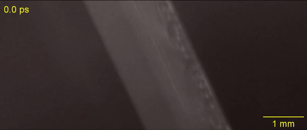
Light moving in vacuum is the fastest thing in the universe. Scientists have tried many times before to catch it on the move with some success. This time a new equipment built by Caltech scientists pulls down a mind-blowing 10 trillion frames per second, meaning it can capture light as it travels along, and also they are working to make it a hundred times faster.
Understanding how light moves through a medium is fundamental to many fields. Keeping that in mind Jinyang Liang and his colleagues are making efforts to make this new contraption or camera as fast as possible. Also, there are potential applications in physics, engineering, and medicine that depend heavily on the behavior of light at scales so small, and so short, that they are at the very limit of what we can measure.
10 trillion fps camera
If a pulse of light can be replicated perfectly, then we could sent one pulse every millisecond and when offsetting the camera’s capture time by an even smaller fraction, like a handful of femtoseconds, then it is possible to capture a single pulse when it is in transition, the next one when it will be a little further, the next one when it will be even further, and so on. The end result is like a movie that’s the same if we captured the transition of first pulse at high speed.
This is highly efficient but not always reliable to count on being able to produce a pulse of light a million times the exact same way. When it is needed to see what happens when light passes through a lens, the camera has to capture the light pulse in real time, which means recording images not just with femtosecond precision, but only femtoseconds apart.
That’s what the new T-CUP method does. It combines a streak camera with a second static camera and a data collection method that is used in tomography.
We knew that by using only a femtosecond streak camera, the image quality would be limited. So to improve this, we added another camera that acquires a static image. Combined with the image acquired by the femtosecond streak camera, we can use what is called a Radon transformation to obtain high-quality images while recording ten trillion frames per second,
explained co-author of the study Lihong Wang.
At any rate, this method allows for images to be captured just 100 femtoseconds apart. That’s ten trillion per second, or it would be if they wanted to run it for that long, but there’s no storage array fast enough to write ten trillion datacubes per second to, so they can only keep it running for a handful of frames in a row for now.
Light captured in slow motion
In the GIF above, those 25 frames show a femtosecond-long laser pulse passing through a beam splitter.
Noticing how at this scale, the time it takes for the light to pass through the lens itself is nontrivial. Taking this into account the level of precision in real time is quite astonishing, but the team isn’t done yet. You can read the research paper published in the Nature journal.
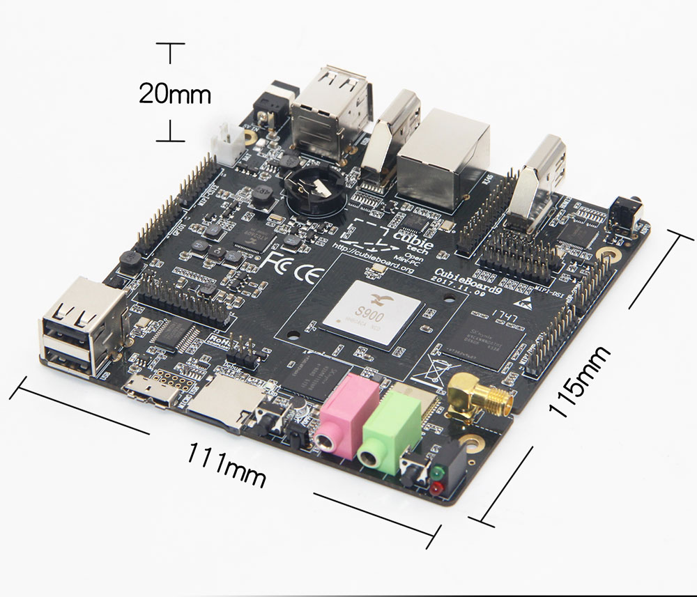
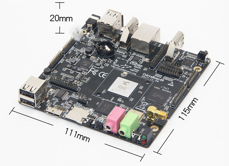
CubieTech recently announced a new SBC CubieBoard9 on their product page. This SBC is yet unpriced and also not reached the CubieBoard.org community website. CubieBoard9 features a quad A53 Actions S900 SoC, 3GB LPDDR3, 16GB eMMC, WiFi/BT, and dual independent displays with HDMI, MIPI-DSI, LVDS, and eDP. Back in 2014, CubieTech announced Allwinner A80 based CubieBoard8 that was never launched in the market for some reason.
The CubieTech became an official distributor of Actions Technology application processors in July 2017 and since then they launched 4 open-source SBCs based on Action SoCs. CubieBoard7, built around the quad-core Cortex-A53 Actions S700, and the CubieBoard6, which instead taps the quad A9 Actions S500 are two of them. They also released the CubieAIO-S700 and CubieAIO-S500, two sandwich-style versions of their Action SoC based SBCs.
The CubieBoard9 integrates 3GB LPDDR3 and 16GB eMMC with a microSD slot. The product page mentions a 10/100 Ethernet port just like the CubieBoard6 and CubieBoard7. It lacks a GbE port for networking. Considering that the CubieBoard4 has a 10/100/1000 GbE port, it looks like a slight downgrade. But in terms of media interfaces, this new SBC is way ahead of its predecessor CubieDroid4. Now you get dual independent displays with a choice of 2x HDMI 1.4 ports for 4K@30 video plus 2x LVDS and single MIPI-DSI and eDP interfaces. These are joined by dual MIPI-CSI connections and dual audio jacks. The CubieBoard9 also provides a wireless module with 2.4GHz/5GHz 802.11b/g/n/ac and Bluetooth 4.1 via an Ampak AP6255 module.
The key features of the CubieBoard9 are:
Processor: Actions Semiconductor Actions S900 (4x Cortex-A53 cores @ up to 1.8GHz), PowerVR G6230 GPU @ 600MHz with OpenGL ES 3.1
Memory/storage:
3GB LPDDR3-800 64-bit RAM (possible option for 2GB)
16GB eMMC
MicroSD slot
Wireless: Dual-band (2.4GHz/5GHz) WiFi 5 (ac) with Bluetooth 4.1 (Ampak AP6255) with ant. connector and ext. antenna
Networking: 10/100 Ethernet port
Display/media I/O:
2x HDMI 1.4a ports at up to 4K @ 30fps
MIPI-DSI
2x LVDS (DSI)
eDP (DSI)
MIPI-CSI
MIPI/DVP-CSI
Dual independent display support
2x audio jacks (mic-in, earphone out); second mic-in header
Other I/O:
USB 3.0 OTG port
4x USB 2.0 host ports
2x GPIO headers
UART header
Other features: IR receiver, RTC with cell battery connector, 2x LEDs, power key, reset key, ADFU key, heatsink, acrylic case kit
Power: 5V DC jack; Li-Po battery connector
Dimensions: 115 x 111 x 18mm
No pricing or availability information was provided for the CubieBoard9. More information may be found on the CubieTech’s CubieBoard9 product page, and more information may eventually appear on Cubieboard.org.
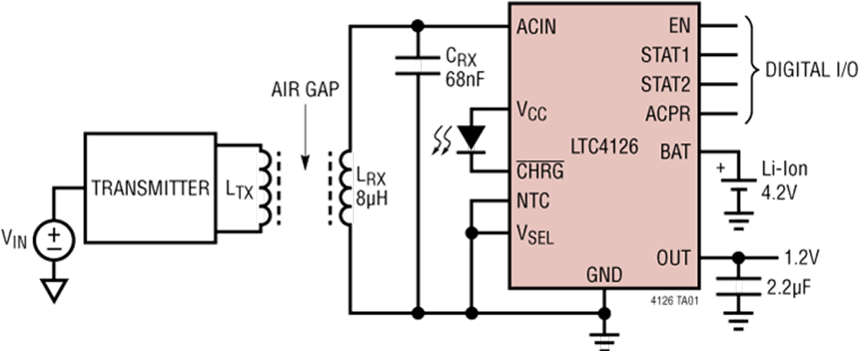
Analog Devices announces the Power by Linear™LTC4126, which expands its offerings in wireless battery charging. The LTC4126 combines a wireless powered battery charger for Li-Ion cells with a high efficiency multi-mode charge pump DC/DC converter, providing a regulated 1.2V output at up to 60mA. Charging with the LTC4126 allows for a completely sealed end product without wires or connectors and eliminates the need to constantly replace non-rechargeable (primary) batteries. The efficient 1.2V charge pump output features pushbutton on/off control and can directly power the end product’s ASIC. This greatly simplifies the system solution and reduces the number of necessary external components. The device is ideal for space-constrained low power Li-Ion cell powered wearables such as hearing aids, medical smart patches, wireless headsets, and Internet of Things (IoT) devices.
The LTC4126, with its input power management circuitry, rectifies AC power from a wireless power receiver coil and generates a 2.7V to 5.5V input rail to power a full-featured constant-current/constant-voltage battery charger. Features of the battery charger include a pin selectable charge voltage of 4.2V or 4.35V, 7.5mA charge current, automatic recharge, battery temperature monitoring via an NTC pin, and an onboard 6-hour safety charge termination timer. Low battery protection disconnects the battery from all loads when the battery voltage is below 3.0V. The LTC4126’s charge pump switching frequency is set to 50kHz/75kHz to keep switching noise out of the audible range, ideal for audio related applications such as hearing aids and wireless headsets.
Features
Wireless Li-Ion Battery Charger with High Efficiency Multi-Mode Charge Pump DC/DC
Wideband Wireless Receive Power Frequency: DC to >10MHz
Integrated Rectifier with Overvoltage Limit
Pin Selectable Charge Voltage: 4.2V or 4.35V
Fixed 7.5mA Charge Current
Low Battery Disconnect (3.0V)
NTC Pin for Temperature Qualified Charging
1.2V DC/DC Regulated Output at Up to 60mA
50kHz/75kHz Switching, No Audible Noise
Pushbutton and/or Digital on/off Control for DC/DC
The LTC4126 is housed in a highly compact, low profile (0.74mm) 12-lead 2mm × 2mm LQFN package. The device is guaranteed for operation from –20°C to 85°C in E-grade. For more information, visit www.analog.com/LTC4126
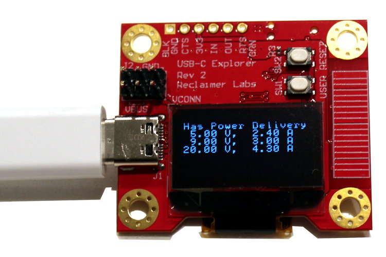
Jason has designed a development board for USB-C and Power Delivery, that is available on GitHub. The board is also on sale at Tindie for $79 + shipping.
The USB-C Explorer is a development board with everything needed to start working with USB Type-C. It contains a USB-C port controller and Power Delivery PHY chip, a microcontroller, and several options for user interaction.
The default firmware will identify as a USB Power Delivery Sink and list out all power capabilities from a corresponding Source. It will then request the highest power option. This voltage will be available on the power header. The example photo shows the capabilities of an Apple MacBook 87W Charger.
The USB-C Explorer helps to get started with USB-C – [Link]
Yep. It works. At least tested pretty thoroughly with my ATTiny10. It can also read all the memories AND run timings against the AVR to do processor clock calibration, as well as fuses and manual poking to flash en post to allow for custom configuration.
This was actually written in two days for Unit-E Technologies and is made available freely. This project is licensable via the newbsd license.
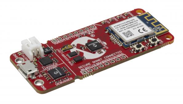
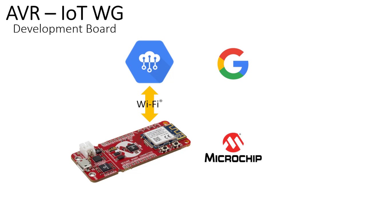
RS Components will stock Microchip’s AVR microcontroller IoT development board for Google Cloud, which enables the fast prototyping of cloud-connected devices. By Ally Winning [via]
The Microchip AVR-IoT WG development board uses an ATmega4808 AVR-based MCU, with a ATECC608A CryptoAuthentication IC and a fully certified Wi-Fi network controller. The board works with Google Cloud IoT Core, which offers an artificial intelligence and machine learning based infrastructure and enables the simple collection, processing and analysis of data, as well as a being a scalable platform for IoT applications.
Developers can add cloud connectivity to a device via a free online portal. Once an IoT device is connected to Google Cloud, engineers can develop and debug applications in the cloud using tools such as Microchip’s MPLAB Code Configurator (MCC) or Atmel START.
The ATmega4808 processor is an 8-bit MCU that features Core Independent Peripherals (CIPs) to deliver low power consumption. It also offers advanced sensing and robust actuation features. The ATECC608A CryptoAuthentication IC comes pre-registered on Google Cloud IoT Core and is ready for use with zero touch provisioning.
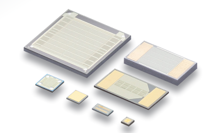
Murata high-density silicon capacitors are developed with a semiconductor MOS process and are using the third dimension to substantially increase the capacitor surface and thus its capacitance without increasing the capacitor footprint. Murata silicon technology is based on a monolithic structure embedded in a monocristalline substrate (single MIM and multi MIM – Metal Insulator Metal).
Higher performance in a smaller package
This advanced 3D topology gives a developed area equivalent to 80 ceramic layers in an amazing 100 µm thickness (lower value on request) of active capacitance area. Thanks to a very linear and low dispersive dielectric, miniaturization, capacitance value and electrical performances are optimized.
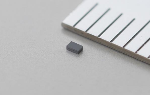
Measuring just 0.9×0.6×0.3mm (50 % smaller than a conventional 32.768 kHz crystal resonator), the WMRAG series 32.768 kHz MEMS resonator is the world’s smallest, claims manufacturer Murata.
Murata Manufacturing Co., Ltd. (Head Office: Nagaokakyo-shi, Kyoto; Chairman of the Board and President: Tsuneo Murata) has developed the world’s smallest 32.768kHz MEMS resonator, which is expected to make a significant contribution to reducing the size and power consumption of IoT devices, wearables, and healthcare devices.
While achieving miniaturization through MEMS technology, the new MEMS resonator exhibits frequency temperature characteristics of less than 160ppm (Operating temperature: -30 to 85°C ) with an initial frequency accuracy (25°C ) that is comparable to or better than that of a quartz tuning fork crystal resonator.
Key features
Over 50% smaller than conventional tuning fork quartz crystal resonators
With dimensions measuring 0.9 x 0.6 x 0.3mm (width, length, height), the new MEMS resonator is more than 50% smaller*6 than a conventional 32.768kHz tuning fork crystal resonator.
Built-in load capacitors
A typical pierce-type oscillator circuit design uses two external multilayer ceramic load capacitors. The new MEMS resonator is equipped with built in load capacitors, which makes possible a reduction in external parasitic capacitance, mounting space, and further contributes to more flexible circuit design.
Reduced power consumption by realizing a low ESR
With crystal resonators in general, the ESR tends to rise as the device becomes smaller in size. However, with a low ESR (75kΩ) the MEMS resonator can generate a stable reference clock signal by reducing the IC gain while also cutting power consumption by 13% compared to a conventional quartz crystal. (Based on internal tests)
Can be built into an IC package
With silicon-based wafer-level chip scale packaging (WLCSP), the resonator can be co-packaged with an IC, eliminating the need for any external low-frequency clock references.
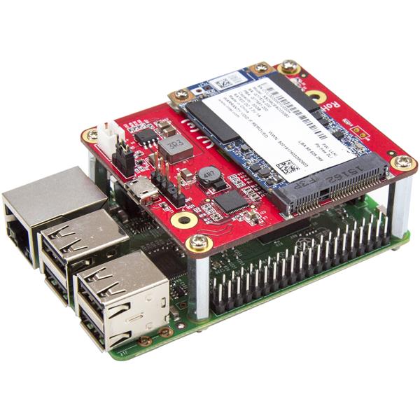
Connect an mSATA drive to your development board, to increase its data storage capacity. [via]
Increase the data storage capacity of your Raspberry Pi or other development board, by connecting it directly to an mSATA drive. Perfect for custom projects and applications, this USB to mSATA converter supports all models of Raspberry Pi as well as other development boards.
This convenient USB 2.0 mSATA converter lets you overcome data storage limitations by enabling you to connect an mSATA drive through your board’s USB-A port.
The USB to mSATA converter integrates seamlessly with your existing development board. It’s the perfect addition for development-board based applications such as surveillance, media players and servers, digital signage and IoT/automation solutions. It allows you to utilize your mSATA drives with your development board, and take advantage of the small form factor of mini-SATA, ideal for applications with space limitations.