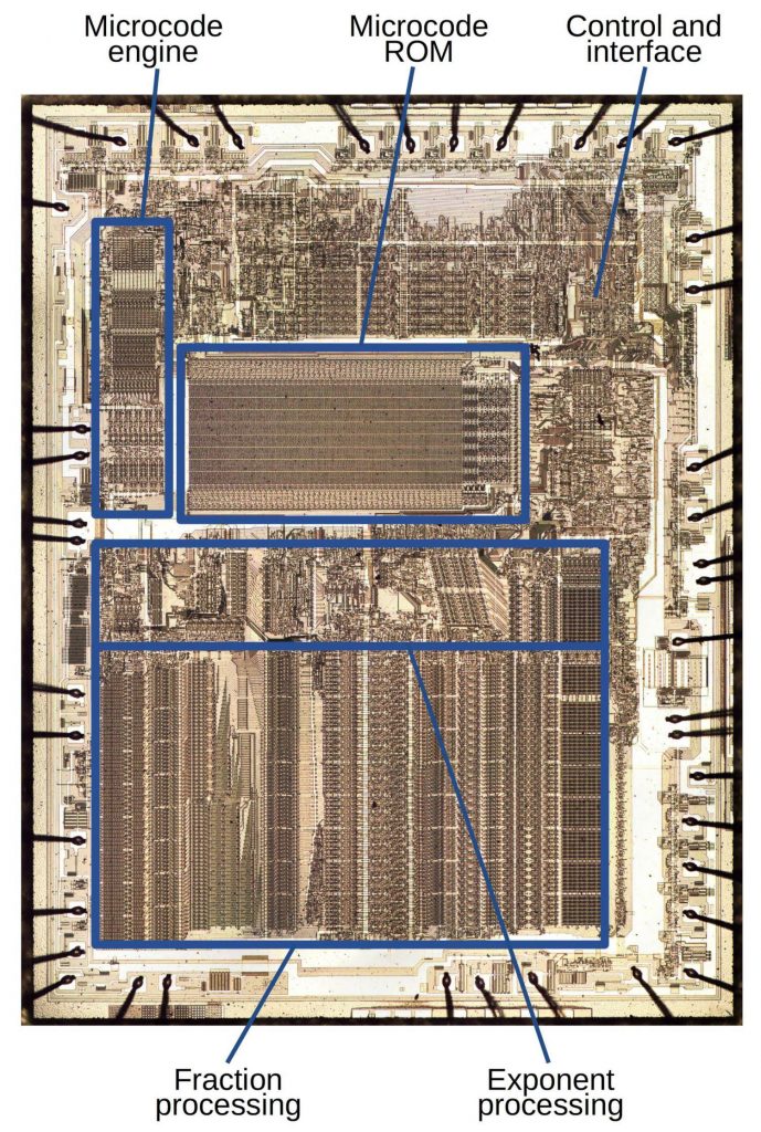
The 8087 chip provided fast floating point arithmetic for the original IBM PC and became part of the x86 architecture used today. One unusual feature of the 8087 is it contained a multi-level ROM (Read-Only Memory) that stored two bits per transistor, twice as dense as a normal ROM. Instead of storing binary data, each cell in the 8087’s ROM stored one of four different values, which were then decoded into two bits. Because the 8087 required a large ROM for microcode1 and the chip was pushing the limits of how many transistors could fit on a chip, Intel used this special technique to make the ROM fit. In this article, I explain how Intel implemented this multi-level ROM.
Two bits per transistor: high-density ROM in Intel’s 8087 floating point chip – [Link]
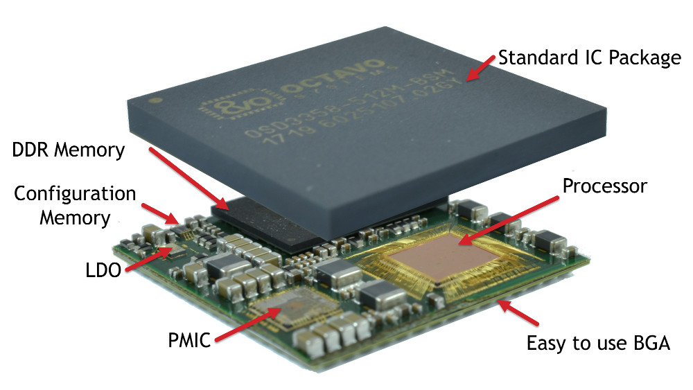
The OSD335x C-SiP System-in-Package (SiP) developed by Octavo, is a concept package that is modeled on its previous Sitara AM335x based SiP by including up to 16GB eMMC, an oscillator along with 1GB DDR3, PMIC, LDO, and EEPROM. The OSD335x C-SiP, is the most consolidated System-In-Package (SiP) module ever made. Modeled like its predecessors, the OSD335x C-SiP incorporates the Cortex-A8 based Texas Instruments Sitara AM3358 SoC with RAM, including the addition of the eMMC and oscillator for the first time and other principal components. The addition of the eMMC and the Oscillator to the processor, RAM and power supplies makes the OSD335x C-SiP a complete system.
Detailed view of the OSD335x C-SiP
The CTO of Octavo Systems Gene Frantz said it has everything one needs for a powerful Linux computer integrated into a small, easy to use package and what is only requires to do is add power and a couple of resistors. That is why it is called a Complete System-In-Package. The advantage of SiPs is that they require less space and someone can achieve easier and speedy development, among other benefits. During an interview with LinuxGizmos, Octavo Systems CTO said they have done most part, by taking on the tedious part of system design for the embedded developers (how to get the processor, memory, PMIC, and other components to work together nicely). With the incorporation of OSD335x C-SiP, many of the monotonous and tedious tasks related to designing a computing system are eliminated. Tasks like laying out DDR3 memory interfaces and power sequencing are no longer needed.
Also, any issue about Electromagnetic Interference (EMI) caused by the layout of the Oscillator is removed. Apart from making a simple design of an embedded system, the OSD335x C-SiP is also about 50% smaller than a corresponding system built with separate components. This allows designers to decrease their design size, save cost on their PCBs, or add processing power to form factors that weren’t possible before. Like the earlier packages, the OSD335x C-SiP offers a TPS65217C PMIC and TL5209 LDO, both from TI. It will also be available in 0 to 85°C and -40 to 85°C models.
The OSD335x C-SiP is packaged with the usual Debian stack and offers open source files including schematics. The design is said to enable full access to AM335x features, including the PowerVR SGX GPU and programmable PRU chips. The module is backwards compatible to the OSD3358-SM-RED, various BeagleBone boards, and other Sitara AM335x hardware. The initial models that are ready for pre-order include the higher-end AM3358 version of the SoC, as well as 512MB of DDR3 and 4GB eMMC. In coming 2019, other models will be fitted including larger memoriy.
The C-SiP may be a bit more expensive than buying the different components separately, but Octavo’s SiP packages have the advantages of not only reducing development cost but also potentially, manufacturing costs. For example, it can reduce the need to add multiple PCB layers or print double-sided boards. Application Engineering Manager of Octavo Systems, Erik Welsh estimated that with the OSD335x C-SiP, designers can get a system working in half the time required to design a discrete solution.
The OSD335x C-SiP can be used in building automation, Industrial Control, Consumers goods, and IoT application.
A Weather station project is a project that gives you information about the weather in a particular area and is quite useful for a lot of things like planning of the day, farming and several others. A weather station project is one of those projects where you can have different types of sensors attached to it. In this post, I will highlight some interesting sensors that can be added to a weather station based project.
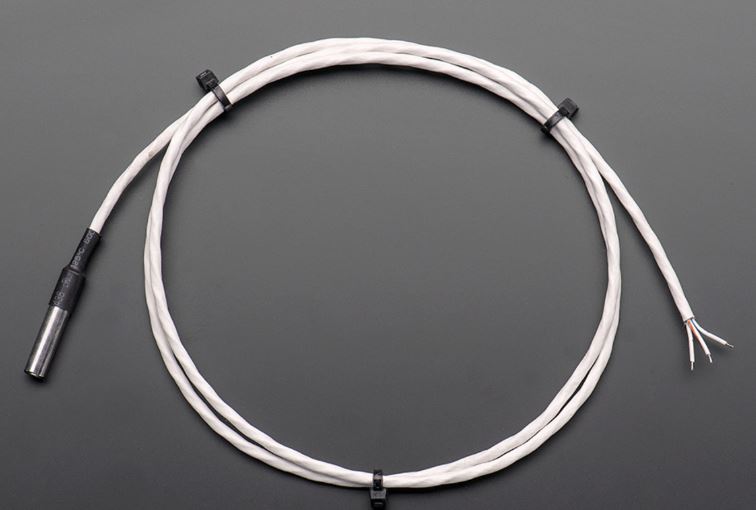
DS18B20 Temperature Sensor
DS18B20
The DS18B20 is a temperature sensor and one of my favorite one. Unlike other temperature sensors, the DS18B20 is one wire type of sensor. It only requires one wire for communication and also supports parasite modes. Parasite mode means it doesn’t need a power supply, and it can get powered from the same data line. One of the features of the DS18B20 and other one-wire sensors is the fact that you connect multiple sensors to just one pin. I have connected about 32 of those sensors to one single digital pin on the Arduino Uno. Continue reading “Interesting Sensors To Add To Your Weather Station Project”
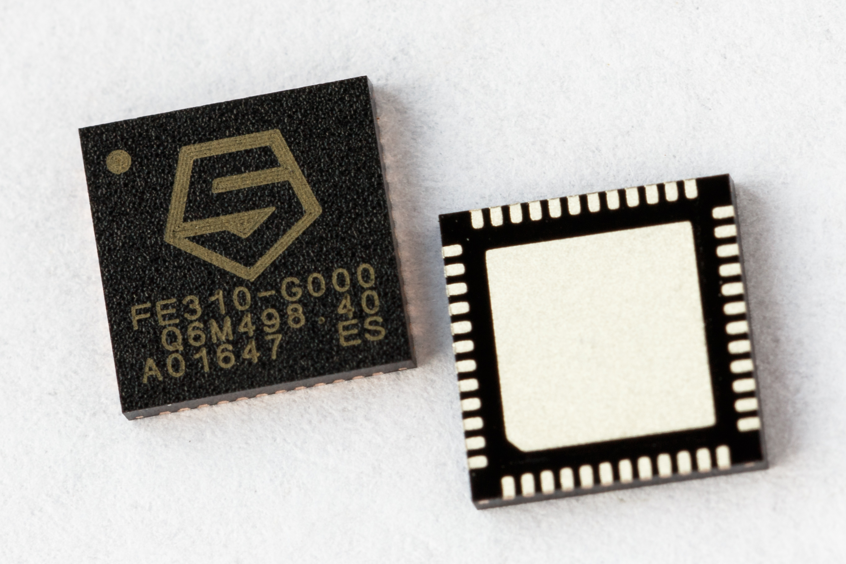
Developed in the dark hours of the night, between 2 and 8 o’clock in the morning of August 19th by Marcelo Samsoniuk, the DarkRISC-V stack is an experimental open source implementation of the RISC-V standard targeting the low-cost Xilinx Spartan-6 family of FPGAs. Following a week of debugging, Samsoniuk has released the implementation to GitHub under a BSD license.
RISC-V First Chip – Freedom everywhere 310 Chip
Marcelo Samsoniuk’s says:
The general concept is based in my other early RISC processors and composed by a simplified two stage pipeline where a instruction is fetch from a instruction memory in the first clock and then decoded/executed in the second clock. The pipeline is overlapped without interlocks, in a way the DarkRISC-V can reach the performance of one clock per instruction most of time (the exception is after a branch, where the pipeline is flushed and one clock is lost). As addition, the code is very compact, with around two hundred lines of obfuscated but beautiful Verilog code.
Although the code is small and crude when compared with other RISC-V implementations, the DarkRISC-V has lots of impressive features:
Implements most of the RISC-V RV32I instruction set.
Works up to 75MHz and sustain 1 clock per instruction most of the time
Flexible Harvard architecture (easy to integrate a cache controller)
Works fine in a real spartan-6 lx9
Works fine with gcc 9.0.0 for RISC-V (no patches required!)
Uses only around 1000 LUTs (spartan-6, core only)
It has BSD license.
With the first GAP8 processor samples by Open-Silicon shipping, we’re almost approaching a period where we have multiple vendors producing open silicon built around the RISC-V core, and when that happens we’ll be in a very different place. At that point, we’re in a real open hardware environment because we no longer have vendor lock in, and it’s going to be interesting to see whether that makes a difference to the availability of boards based on RISC-V.
Until then, however, the availability of implementations of the RISC-V architecture, and the ability for people to get hands on with it—whether that’s using an FPGA or not—is important to the ecosystems continued health.
For instructions on how to implement RISC-V visit its GitHub Repository.
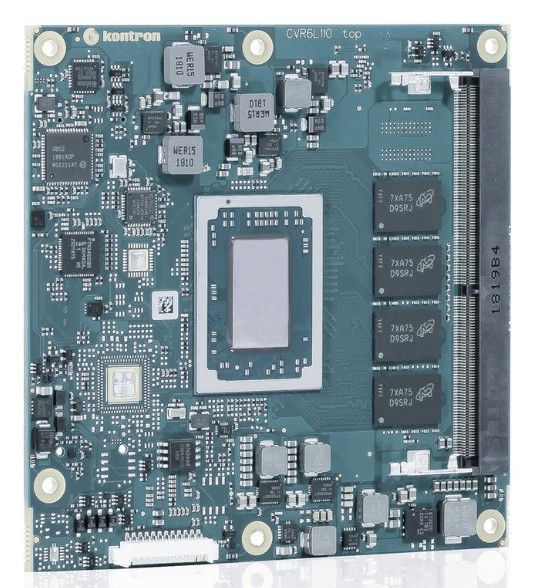
Kontron a global provider of IoT/ Embedded computer Technology (ECT) introduces its Linux friendly “COMe-cVR6” Express Type 6 module, that comes with a Ryzen embedded V1000 SoC with up to 24GB DDR4, including 8GB soldered on board. The board also comes with a quad- display support and optional- 40 to 85-degree Celsius operation and security features.
Kontron Module Powered by AMD Ryzen V1000 Chip
The COM Express compact module’s smaller form factor significantly saves space in comparison to most comparable solutions, allowing developers to create more compact designs with higher performance. Variants of the COMe-cVR6 (E2) are also resistant to vibration and shocks due to the permanently soldered memory, just as all other components, such as voltage smoothing capacitors, and controllers are selected for highest resistance to environmental stresses.
The new module is particularly suitable for applications in harsh environments, medical or industrial image processing systems. This product runs Linux or Windows 10. The new COMe-cVR6 adopts the 95x95mm COM Express compact Type 6 form factor. In COM Express Compact modules, external I/Os are placed next to the module instead of attaching them on the underside of the carrier board when using a larger basic form factor.
This allows the main board height to be reduced by up to 2cm. The new AMD Ryzen V1000 processor combines the extremely powerful Zen micro processor architecture with the new AMD Radeon Vega graphics supporting up to 11 compute units. The AMD Ryzen Embedded V1000 processor offers up to twice the performance than the previous versions and delivers up to 46% more multi- thread performance than competitive solutions. Other COM Express compact modules with the V1000 SoC includes Seco’s COMe-B75-CT6. V1000 based basic modules include Congatec’s Conga-TR4 and Advantech’s SOM5871.
The new APU offers a comprehensive feature set for data and application security. The built in AMD secure processor handles hardware- accelerated data encryption and decryption for secure virtualization, secure encrypted virtualization (SEV) isolates the hypervisors and virtual machines without having to modify any of the code. The Ryzen Embedded V1000 competes with intel’s 14nm- fabricated core processors.
The SoC offers up to four dual-threading Zen CPU cores for 8 threads total, as well as high-end Radeon graphics with up to 11 compute units. The COMe cVR6 supports all five quad and dual core models including the quad core V1404i model, which was missing from AMD’s original announcement, but is supported by the Seco and Congatec modules.
The V1404i lacks the other SoC variants’ dual threading but has a low 15W TDP. The COMe-cVR6 features dual SATA III interfaces, as well as an SDIO connection shared with GPIO. If you choose to skip the default GbE controller, you can get 6x PCIe 3.0 connections instead of the standard 5x interfaces.
There’s also an option for a PCIe switch in place of one of the PCIe interfaces and an “on request” option for 8x PCIe x1 (4x PCIe 3.0 plus 4x PCIe 2.0), along with 1x PEG x8. Four independent displays are supported, tapping a special capability of the V1000’s Vega graphics. Kontron did not mention resolution, but 4K should be available with the dual DisplayPort++ links if not the standard DisplayPort with optional VGA.
The fourth interface is a lower-resolution, dual-channel, 18/24-bit LVDS, which can be swapped out for eDP. The COMe-cVR6 is further equipped with 1x USB 3.0, 2x USB 3.1 Gen2, 5x USB 2.0, and 2x RX/TX only serial ports. Other interfaces include HD audio, I2C, LPC, SPI, and SMBus. You also get a staged watchdog timer, a real-time clock, TPM 2.0, and optional Kontron Apportect security. The latter includes a Wibu-Systems security chip and a software framework with IP- and copy/reverse engineering protection.
No pricing or availability information was provided for the COMe-cVR6. More information may be found in Kontron’s COMe-cVR6 announcement and product page.
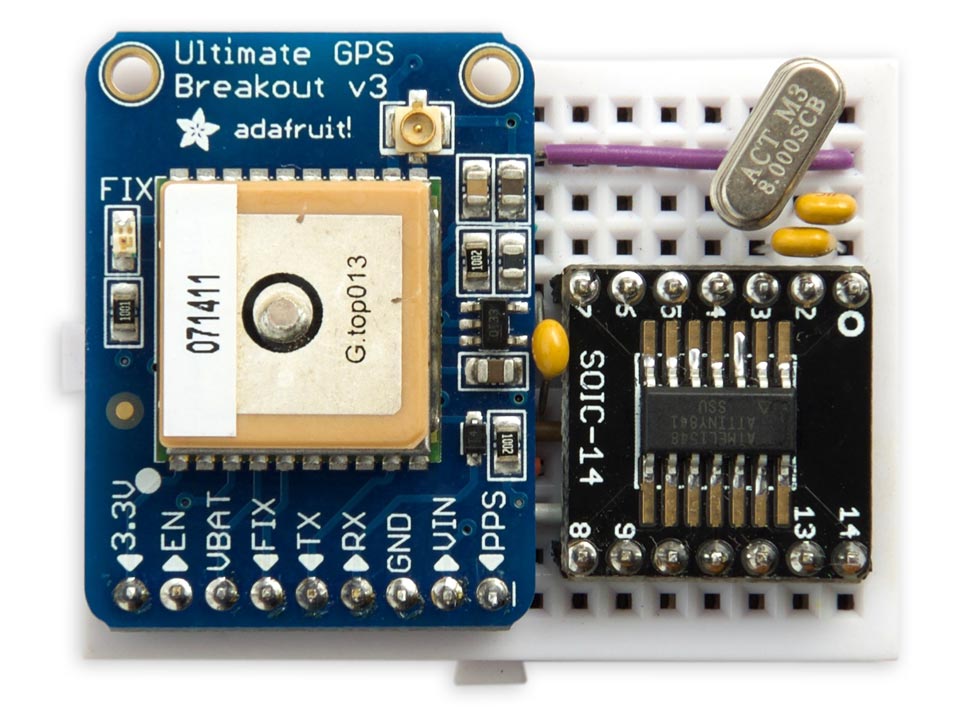
GPS module with an I2C interface, provided by an ATtiny841.
This project describes a simple GPS module which you can interface to via I2C. It uses an ATtiny841. David Johnson-Davies writes:
Incorporating GPS into a project is quite daunting. First you have to parse the NMEA sentences from the GPS module you’re using, and then if you’re doing any calculations with the received longitudes and latitudes, you need to incorporate a floating-point GPS library with routines to perform the calculations.
If you need to do any other significant processing there’s a chance that the GPS handling may interfere with your other tasks. Providing the GPS processing as a separate I2C module solves this problem.
I originally designed this to provide GPS support to boards running my Lisp interpreter, uLisp, but it could be useful for any other application where you want GPS data accessible via a simple I2C interface. It is based on my earlier project Making Your Own I2C Peripherals which described how to make an I2C slave device based on an ATtiny841.
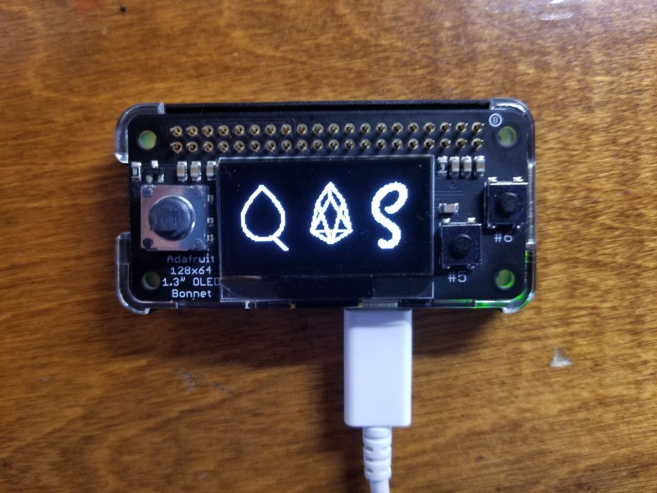
Liquid EOS in collaboration with Scatter (SSO authenticators) have recently invented the first open source EOS Hardware Wallet, which provides secure storage of blockchain based cryptocurrency. This device could be built from the comfort of your home. They have provided a step-by-step guide on how to build your own affordable Hardware Wallet for around $41 with off- the shelf parts.
Open Source Liquid EOS Hardware Wallet
The EOS Hardware Wallet is a relatively simple design that features a Raspberry Pi Zero W, an Adafruit 128×64 OLED Bonnet, a Pi Zero enclosure, and a 16GB micro SDHC card for storing EOS cryptocurrency. If you want to embark on building the Hardware, you have to be skillful with the soldering iron or otherwise you could go with a Zero WH that is already outfitted with pre-soldered pins.
Assembly of the hardware is pretty straightforward. Just connect the Bonnet to the Zero using the 20- pin header, then place the electronics inside the enclosure, install the microSD card and you are ready to move onto the software side. Regarding software, the hardware Wallet makes use of Liquid EOS Bancor based blockchain software that uses a protocol to keep tabs on your EOS cryptocurrency. Scatter Desktop is used to keep everything secure, authentication, permission, identities, blockchains, and currency and comes with an SSO that uses asymmetrical encryption.
The advantages of Hardware Wallets includes immunity to computer viruses that can steal money from software wallets. Also, the private key information will never be exposed to the working system and will be kept safe within the Hardware Wallet. Although the EOS Hardware Wallet is open source and Scatter is trusted to keep everything secure, there are several disclaimers to this device.
Your private key safety is as strong as your Wallet password.
Importing the seed phrase is not supported yet.
No Hardware encryption yet.
We are going to add encryption with a second key- entered in the Scatter Desktop App.
The transaction details info is currently trusted by the Scatter Desktop App.(This will be fixed in future releases).
Only key pair is currently supported.
This is an alpha. Do not use this Wallet for your “owner” keys.
Please wait a while before using it on mainnet until we and the community test it a little more. If you choose to create your own Hardware, visit Liquid EOS medium page for a complete step by step walk through on building an EOS Hardware Wallet, complete with BOM, and software files and firmware.
Munich, September 26, 2018 — SimScale, the provider of the world’s first production-ready SaaS application for engineering simulation (CAE), announced today the release of their new workbench.
The new and improved SimScale Workbench 2.0 was built entirely from scratch on the latest, state-of-the-art technology stack, with the goal of drastically improving user productivity by decreasing loading time and increasing interaction speed.
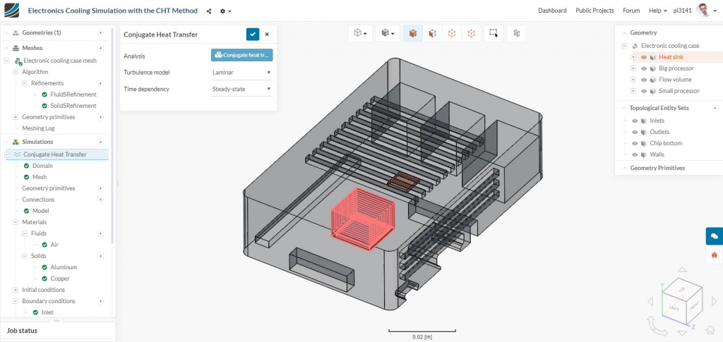
Figure 1: Screenshot of the SimScale Workbench 2.0
With this update, the SimScale web-based CAE platform is now as fast and interactive as a desktop application, while taking advantage of the unlimited computing power of the cloud. Furthermore, the new solution stack sets the stage for major new updates and features that are already in development and will be released in the coming months.
Right from the start I love it! Well done. This is a really nice improvement,
said Ben Lewis, President at Custom Machines and SimScale customer.
SimScale was built to bring simulation technology to every designer and engineer in the world. With the release of the new workbench, we take a big leap towards making CAE as easy as it needs to be to emerge from the expert’s toolbox into a web-based platform everybody can benefit from. Some exciting automation features are yet to come, so keep an eye on us,
said Alexander Fischer, VP Product and co-founder of SimScale.
In addition, the latest release from SimScale introduces some fundamental changes to the overall user experience, making the SimScale Workbench 2.0 the most advanced, yet user-friendly simulation interface version ever created by the cloud simulation company.
Compared to the old workbench, with the new version the viewer takes up significantly more screen real estate, becoming the heart of the interface. To improve the overall user experience, the settings panels now ‘float’ on top of the viewer, reserving as much space as possible for visualization. Together with a new model color scheme—which preserves the original CAD coloring if possible—and a translucent render mode, interaction with the model has been made significantly more efficient.
Figure 2: Conjugate heat transfer simulation of an electronics enclosure with SimScale
SimScale’s vision includes making engineering simulation as intuitive as possible. With the previous workbench, the meshing, simulation and post-processing steps were separated into three different tabs. The new version, on the other hand, consolidates the entire workflow into a single tree, helping users set up their projects faster and easier by following a straightforward, step-by-step approach, from top to bottom.
A third major change is the possibility for users to carry out a simulation directly on a CAD model. In practice, this means the user can now set up a complete simulation directly on their geometry with less exposure to mesh generation—something that will particularly help novice users to successfully simulate faster. The added benefit of this approach is that, in the case there is a need to change or refine the mesh, all settings and assignments will be kept.
More details regarding the new features that the release of SimScale Workbench 2.0 brings can be found on the SimScale Blog.
Since the platform’s official launch in 2013, SimScale has been challenging the “status quo” of the traditional computer-aided engineering (CAE) software market by offering a fully cloud-based engineering simulation solution with zero hardware and software footprint, available at a fraction of the cost of its competitors.
SimScale offers a Community plan which is free to all users willing to share their projects publicly. The Professional plan can be tested via a free 14-day trial. Getting started with the trial only takes a few minutes and only requires a standard web browser.
Electronics designers can boost their productivity with free symbols & footprints for Samtec products
Samtec is releasing new digital models for over 100,000 of its products on SnapEDA, the industry-leading circuit board design library.
Traditionally, designers have spent days creating digital models – such as symbols and footprints – for each component in their designs. Connectors are especially time-consuming to create models for, due to their non-standard shapes, pitches, pads, and cutouts.
With this new collaboration, designers can now easily discover, download, and design with over 100,000 ready-to-use Samtec connector models, helping accelerate the design process. The new models include USB, card edge, board-to-board, headers, and RF coaxial connectors.
Created by Samtec’s Signal Integrity Team, these detailed, high-quality models include accurate assembly, silkscreen and 3D features to support high density applications. The footprints employ courtyards, built-in dimensioning, and applicable metadata.
We pride ourselves on being the service leader, which means investing the time and energy into providing models that expedite the design process for SnapEDA users,
said Greg Horlick, ECAD Systems Architect, at Samtec.
Downloading the printed circuit board (PCB) models is simple: designers create a free account on the SnapEDA website, and then can download for free. Samtec has made the files available for OrCad, Allegro, Eagle and PADS, and using SnapEDA’s translation technology, the files can also be downloaded for Altium, KiCad, PCB123, Proteus 8.8, and Pulsonix.
Samtec is one of the most in-demand connector manufacturers on SnapEDA, so we know that designers will benefit greatly from these new PCB libraries to bring their products to life faster,
said Natasha Baker, CEO and Founder of SnapEDA.
Their commitment to quality and compliance ensures the reliability that professionals on our platform are looking for in their connectivity solutions.
SnapEDA has a trusted reputation in the market for quality, which makes them an excellent partner for Samtec. Together, we’re ensuring that engineers can quickly discover and more easily design Samtec parts into their systems. Our model library is constantly expanding, and we’ve been wowed by the speed and support SnapEDA has provided in delivering these to their users,
said Daniel Williams, Digital Marketing Director, at Samtec.
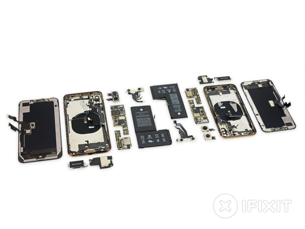
The teardown of the latest Apple iPhone XS is showing the key suppliers and a new battery design. [via & via]
The teardown by iFixit shows a single cell battery pack that is L-shaped to fit into the spare space in the handset. The XS has a 10.13 Wh battery (2,659 mAh at 3.81 V), weighing 39.5 g, slightly downgraded from last year’s iPhone X. The larger XS Max uses the same dual cell battery design that was introduced with the iPhone X.
Patents from 2014 show the ways Apple as addressed the thermal expansion of the L-shaped cell, using different layer sizes and precisely folding electrode sheets cut into complex shapes to fit those contours.
The teardown also shows the key suppliers of power chips for the new design in both the XS and XS Max.
Apple’s APL1W81 A12 Bionic SoC is layered over Micron MT53D512M64D4SB-046 4 GB LPDDR4X SDRAM with power management from an STMicroelectronics STB601A0 and Apple 338S00383-A0 power management IC provided by Dialog Semiconductors. There is also an another power management IC, the Apple 338S00456, and another Dialog chip for system power management, the Apple 338S00375.
A Cypress CPD2 is used for the USB power delivery, alongside a Texas Instruments 61280 battery DC-DC converter, and a separate charging board hosts TI’s SN26