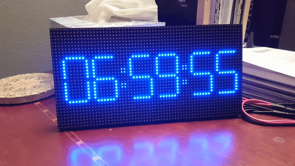
Thanks to the work of the Arduino and ESP8266 community, this cool clock is a surprisingly easy to build! Follow the detailed instructions to build your own.
Just two main components: Display (obviously) and a WiFi MicroController
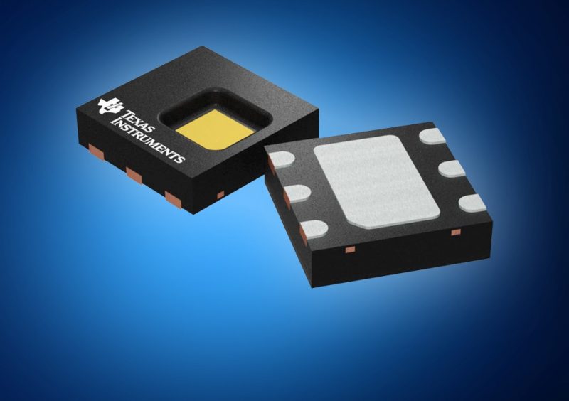
Distributor Mouser Electronics has added Texas Instruments’ HDC2080humidity and temperature digital sensor. It offers high accuracy and low power consumption in a compact package, reports the distributor and is suitable for a range of IoT and environment monitoring applications.
The TI HDC2080 humidity and temperature digital sensor is a capacitive-based device that uses an integrated heating element to dissipate moisture and condensation. The sensor integrates multiple digital features, allowing for the use of programmable input thresholds to deliver system wake-ups and alerts without needing to rely on a microcontroller to monitor the system. The HDC2080 sensor’s low power consumption allows developers to place their microcontrollers in deep sleep mode, because the sensor can initiate measurements without input from a microcontroller. The high-performance sensors offer a typical humidity accuracy of ± two per cent and a typical temperature accuracy of ±0.2 degrees C.
The sensor features an auto-measurement mode to initiate humidity and temperature measurements, enabling efficient performance in applications with power-budget restrictions. The sensor is designed for battery-operated systems and supports a supply voltage range of 1.62 to 3.6V. With an operating temperature range of minus 40 to 85 degrees C, the sensors can be safely used in applications such as home appliances, smart home devices, smart thermostats, HVAC systems and inkjet printers.
The HDC2080 humidity and temperature digital sensor is supported by the HDC2080EVM, a simple plug-and-play platform that features an MSP430F5528 microcontroller and a USB interface, for communication between the HDC2080 sensor and a PC. The module’s included software graphically logs humidity and temperature data, and the module also allows access to the sensor’s configuration registers.
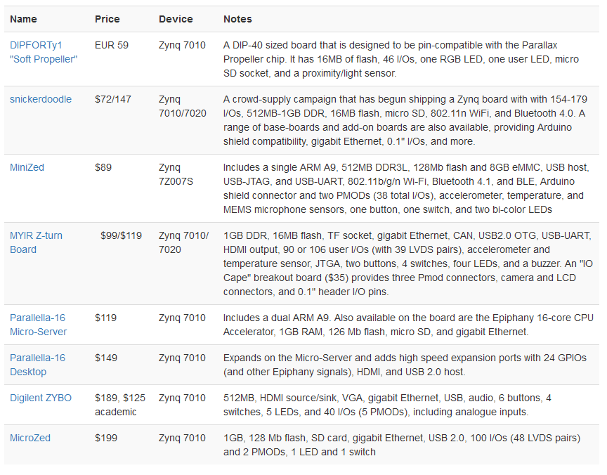
joel @ joelw.id.au has compiled a list of the cheapest available FPGA development boards. The list contains many boards from various manufacturers. He writes:
When choosing a development board, consider what you get with it and what you want to use it for. FPGAs are ideal for use with high speed peripherals, and in general it is much easier to buy a board that contains the part you want, rather than trying to add one on later (and inevitably giving up and upgrading to a more capable board).
[…]
I like having a board with many (at least 8) SPST switches and LEDs, and momentary buttons. Unlike a microcontroller where it’s relatively easy to spit debug information out of a serial port or to an LCD with a single C function call, debugging FPGA designs is a bit harder. LEDs provide a zero fuss way to break out internal signals for visualisation – if you’re tracking the progress of a complex state machine, you can light up an LED when it gets to a certain point without adding any extra logic. While these are easy enough to add yourself, I find that it’s better to get a board that has them so that you don’t waste valuable user IOs or waste time investigating failures caused by your terrible soldering skills.
(Taipei, Taiwan – August 21, 2018) – AAEON, a leading developer of advanced embedded controllers, releases the PICO-APL4, a compact and cost-effective SBC. The PICO-APL4 features onboard memory and storage along with dual Gigabit Ethernet support, and it’s ideally suited for factory automation and IoT gateway systems.
AAEON’s latest PICO form factor board is powered by an Intel® Atom™, Pentium® N4200, or Celeron® N3350 processor. By fitting the controller with up to 4GB of onboard DDR3L memory and up to 64GB of onboard eMMC storage, AAEON has not only made the board more resistant to the shocks and vibrations regularly experienced in industrial settings, but it’s also cut application development times as customers don’t need to test the compatibility of external memory and storage.
The flexible PICO-APL4 houses USB ports and connectors, COM ports, a HDMI port and optional eDP. There’s also a 4-bit DIO to manage peripherals and an optional four-lane MIPI-CSI. Expansion is easily achieved with M.2 B and E keys enabling the connection of additional storage and WiFi/Bluetooth modules. Through an optional board-to-board interface, customers can also extend the IO interface and add a larger DIO.
The PICO-APL4 is designed to give users everything they need for effective factory automation and IoT Gateway applications,” said Jones Huang, AAEON embedded computing division product manager. “Its combination of dual Gigabit Ethernet support with onboard memory and storage put it ahead of almost every competing board, and its flexibility and expansion options ensure that the PICO-APL4 can’t be matched.
SolidRun releases ClearFog GT 8K; a high-end computing, Virtual Customer Premises Equipment to deliver network services such as routing, firewall security and virtual private network connectivity to enterprises. The Clear Fog family has the Clear Fog Pro, Clear Fog Base and now the Clear Fog GT 8K which has taken a little of the other SBCs (Single Board Computers) in the family and has made certain modifications.
ClearFog GT 8K
At the heart of the ClearFog GT 8K is the quad-core Marvell’s ARMADA A8040 SoC, running at a speed of 2GHz and some other co-processors like DMA, XOR, and, others. Ideally, it is expected for the ClearFog GT 8K to share some similar traits with its other ClearFog boards, but it has less in common with them. The Marvell’s Armada 8040 SoC features a networking accelerator with a security co-processor, enabling the ClearFog GT 8K with “full” virtualization support as claimed by SolidRun.
The launching of ClearFog GT 8K means that SolidRun has now upgraded its entire ClearFog family with this newer networking board, powered on the same ARMADA A8040 processor as on the community board, and offering support for up to 16GB RAM, 6 network interfaces, including one 10GbE Small Form-Factor Pluggable Transceiver (SFP+) cage which is useful for telecommunication or data communications applications, and three PCIe slots. There is also the presence of a small RTC or CMOS battery that maintains the time, date, hard disk and other configuration settings in the CMOS memory when the main battery is removed.
ClearFog GT 8K offers vast application potential as a versatile networking solution with a large variety of interfaces. It also allows network functions virtualization and high-end edge computing. The 177 x 110mm measured ClearFog GT 8K is larger than the ClearFog Base but smaller than the ClearFog Pro. It offers an extended 0 to 70°C operating range and adds a -40 to 85°C option. Showing its difference with its family, the ClearFog Pro has a 12V DC input as compared to the wide-range input found on the ClearFog Base and Pro.
This Single Board Computer is capable of running the Linux Kernel version 4.4x, Ubuntu 16.04, and Google IoT Core for easy connection to the Google Cloud Platform.
Below are specifications for the ClearFog GT 8K SBC
Processor — Marvell Armada 8040 (4x Cortex-A72 cores @ up to 2GHz); packet, security, DMA, and XOR co-processors
Other features — User push buttons; LEDs; heatsink; RTC with battery; optional enclosure
Power — 12V DC input
Operating temperature — 0 to 70°C or -40 to 85°C
Dimensions — 177 x 110mm
Operating system — Linux 4.4x; Ubuntu 16.04; Google IoT Platform
There are four different models available. They vary in price due to the kind of eMMC and RAM embedded in each one. The starting price is $209 which comes with 8GB eMMC, the next type comes with 128GB eMMC, and it costs $304, the third one costs $526 and has 8GB eMMC with 16GB RAM, and the last one which goes for $621 has 128GB eMMC with 16GB RAM. As compared to most SBCs in the market, the ClearFog GT 8K is a closed-spec, commercial board. More information about the product can be found on the SolidRun’s ClearFog GT 8K product, wiki, and shopping pages.
Alpha & Omega’s high efficiency and simple to use regulators are designed for automotive, telecom, and networking equipment
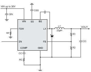
Alpha & Omega Semiconductor’s AOZ128x series are high efficiency, simple, step-down regulators ranging from 0.6 A to 4 A of continuous output current. These EZBuck regulators work from a 3 V to 36 V input range depending on the device. They also offer an adjustable output voltage down to 0.8 V. The fixed switching frequency of 1 MHz PWM operation in the AOZ1282 and 1.5 MHz PWM operation in the AOZ1281 allow for a reduced inductor size, while the AOZ1284 offers a switching frequency of 200 kHz to 2 MHz with an external resistor. The AOZ1284 also offers an integrated N-channel high-side power MOSFET.
These regulators feature internal soft start as well as an adjustable soft start (AOZ1284). The devices support fault protection including thermal shutdown, short-circuit protection, and cycle-by-cycle current limit. The EZBuck series are offered in SOT23-6L, DFN 2×2, and EPAD SO-8 packages making them ideal for automotive, telecom, and networking equipment.
Features
3.0 V to 36 V operating input voltage range
0.6 A to 4.0 A continuous output current
Up to 95% efficiency
Adjustable output voltage range from 0.8 V to 30 V
Cycle-by-cycle current limit
Short-circuit protection
Overvoltage protection
Overtemperature protection
Adjustable switching frequency from 200 kHz to 2 MHz (AOZ1284)
Internal soft start
Available in SOT23-6L, DFN 2×2, and EPAD SO-8 packages
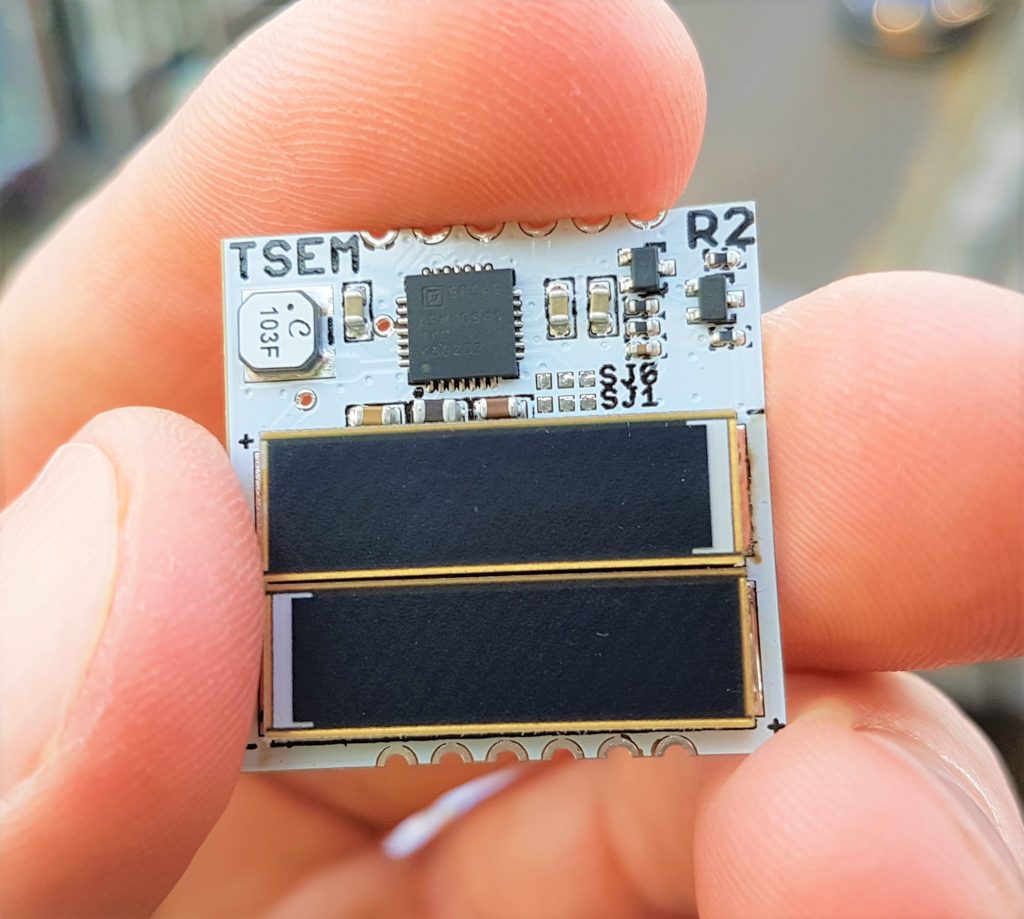
A 1 square inch PCB module with 2 tiny solar cells, a highly efficient Li-Ion charger and with 3.3V and 1.8V output by Jasper Sikken:
This is a 1×1 inch PCB module with two tiny solar cells, a highly efficient Li-Ion battery charger and with two regulated outputs (3.3V and 1.8V). It is unique because it is an easy to manufacture tiny module that other hackers can drop in their PCB design or bread board. Bessides it harvests enough power from indoor light to power a simple BLE or LoRa sensor.
The challenge is to design a TINY module that easily interfaces to other projects. I selected tiny surface mount solderable solar cells, a highly integrated energy harvesting IC, and left out the battery. The board has castellated vias so it can be surface mount soldered onto a mother PCB as well as soldered onto 0.1″ headers to be used in a bread board.
While building Arduino or any other microcontroller platform project over time the need will arise to establish communication between two of the Arduino boards or microcontrollers for data exchange and/or control. This communication could be achieved using either wired or wireless process. For wireless communication between devices, quite a number of options exist including WiFi, GSM/GPRS, Bluetooth, RF and more recent technologies like LoRaWAN among others. All of these communication protocols have their pros and cons and the situation is in which they are the best fit. For mid-range communication between two microcontrollers, for example, one of the most suitable communication protocol is RF (radio frequency) as it has a good cost to performance ratio and a very good communication range can be attained using certain modules.
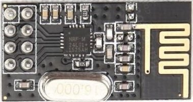
Today, we will look at the radio frequency based communication between microcontrollers using one of the most popular RF communication modules; the NRF24L01 communication module.
The NRF24L01 module is a low-cost (less than$3) ultra-low power, bi-directional transceiver module. It is designed to operate within the 2.4GHz ISM band which means it can be used for projects with industrial, scientific and medical applications. The module can achieve data rates as high as 2Mbits! and uses a high-speed SPI interface in order to communicate with the Arduino and other kind of microcontroller and development boards.
Communication Between Two Arduinos Using NRF24L01 – [Link]
While building Arduino or any other microcontroller platform project over time the need will arise to establish communication between two of the Arduino boards or microcontrollers for data exchange and/or control. This communication could be achieved using either wired or wireless process. For wireless communication between devices, quite a number of options exist including WiFi, GSM/GPRS, Bluetooth, RF and more recent technologies like LoRaWAN among others. All of these communication protocols have their pros and cons and the situation is in which they are the best fit. For mid-range communication between two microcontrollers, for example, one of the most suitable communication protocol is RF (radio frequency) as it has a good cost to performance ratio and a very good communication range can be attained using certain modules.
Today, we will look at the radio frequency based communication between microcontrollers using one of the most popular RF communication modules; the NRF24L01 communication module.
The NRF24L01 module is a low-cost (less than$3) ultra-low power, bi-directional transceiver module. It is designed to operate within the 2.4GHz ISM band which means it can be used for projects with industrial, scientific and medical applications. The module can achieve data rates as high as 2Mbits! and uses a high-speed SPI interface in order to communicate with the Arduino and other kind of microcontroller and development boards.
NRF24L01 module
One of the best features of this module, aside from the ease with which it can be used with Arduino and other microcontrollers, is its low power consumption. This module consumes, less than 14mA in full communication mode and consumes only a few microamps in power down mode. This makes it ideal for projects with long battery life specifications.
To demonstrate the use of this module with Arduino, we will build a simple transmitter and receiver project. The transmitter sends data at a regular interval to the receiver which displays the received data on the serial monitor. This dummy data being transferred could be data from sensors in a real life application or signals to get the receiver to perform certain actions.
Required Components
The following components are required to build this project;
The exact components used for this tutorial, as usual, can be bought via the links attached to them.
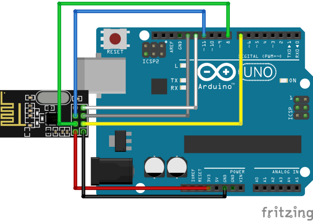
Schematics
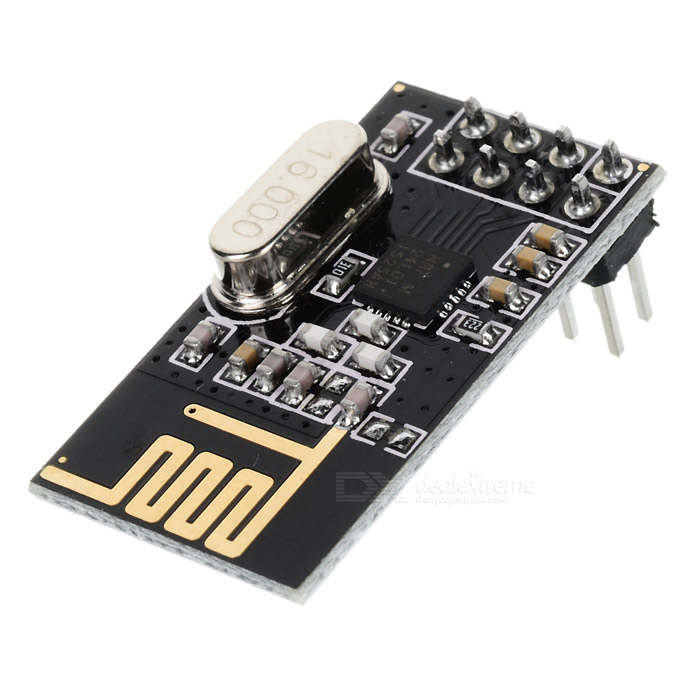
The schematics for this project is quite simple, all we need to do is to connect the NRF24L01 to the Arduino. The NRF24l01’s design is not breadboard friendly, so we will have to connect it to the Arduino with jumper wires.
Connect the components as shown in the schematics below.
Schematics
Don’t forget that the same component will be used to build both the transmitter and receiver so we only need to replicate this for the receiver too.
To make the connection easier to follow and implement, a pin map showing which pins of the Arduino to which the RF module is connected, is shown below.
It’s important that the NRF24L01 module’s VCC pin is not connected to the Arduino 5v pin as this will damage the NRF24L01 module. It is a 3.3V device.
Code
We will write two different Arduino sketches for this project. One of the sketches will be for the transmitter and the other one, for the receiver. The transmitter sketch basically performs the task of sending data at time intervals to the receiver which after receiving the message, prints it on the serial monitor. Both the transmitter and the receiver code are heavily reliant on the RF24 library which can be downloaded from here.
To do a brief explanation of the code starting with the Transmitter, the first thing we do, as usual, is to include the libraries that we will be using for the sketch which in this case is the SPI library which comes with the Arduino IDE and the RF24 library mentioned above.
#include <SPI.h>
#include "RF24.h"
Next, we create an instance of the RF24 library with the pins of the Arduino to which the CE and the CS pins of the NF24Lo1 are connected as arguments.
RF24 myRadio (7, 8);
Next, we create the struct package which is basically a function to package the data to be sent after which we move to the void setup function.
struct package
{
  int id=1;
  float temperature = 18.3;
  char  text[100] = "Text to be transmitted";
};


typedef struct package Package;
Package data;
Under the void setup function, we initialize the NRF24L01 module setting communication parameters like power level, channel, and data rate. It is important to pay attention to the channel used on the transmitter as the same channel needs to be used on the receiver.
With the above done, we then write the void loop function.
The void loop function generates the dummy data to be sent to the receiver by increasing the value assigned to the dummy variable temperature in the struct package by 1 every time the loop runs. After generating the data, it is sent to the receiver using the myradio.write() function which is located at the beginning of the loop.
The second sketch for the receiver is similar to the first, this sketch receives data from the transmitter and displays it on the serial monitor. We start this sketch also by including the libraries that are needed for it.
#include <SPI.h>
#include "RF24.h"
Next, we create an instance of the RF24 library also with the pins of the Arduino to which the CE and CS pins of the NRF24L01 is connected after which we create the struct package to which the temperature data is received.
Next, is the void setup function. Just as we did for the transmitter’s sketch, we will initialize the RF module setting the communication parameters to match the parameters in the transmitter sketch.
With the above done, we write the void loop function. The void loop function for the receiver is fairly simple when data is available, we read the data using the myRadio.read function and display it on the serial monitor.
The complete sketch for both the transmitter and receiver is attached to the zip file under the download section
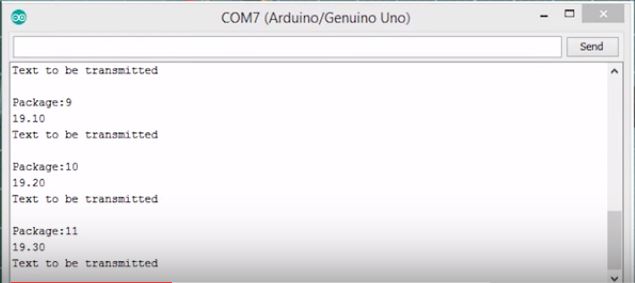
Demo
Upload the corresponding sketch to each board and keep the board on which the receiver code is running connected to the computer so you can view the data being displayed over the serial monitor. After a while, you should see the data from the transmitter being displayed on the serial monitor as shown in the Image below.
Serial Output
All though we used dummy data for this tutorial, this could have been a real-life data being sent from one Arduino to the other providing a solution to a real-life problem. That’s it for this tutorial guys, let me know via the comment section if you build any cool stuff based on this tutorial.
The video version of this tutorial can be watched on youtube here.
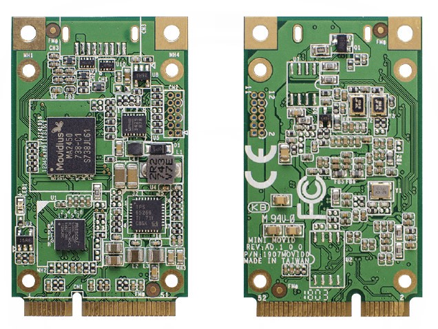
Popularized as the “first embedded ultra-compact artificial intelligence processing card,” and built around the same Intel Movidius™ Myriad™ 2 2450 VPU as Intel’s own Neural Compute Stick. UP’s AI Core is a mini-PCI Express module that enables Artificial Intelligence on the Edge.
The UP AI Core board
The UP AI Core has 512MB of DDR SDRAM and 4 GB of onboard storage. It is a standard looking PCI-e board measuring 51×30 mm. The onboard Movidius™ chip supports the use of both TensorFlow and Caffe frameworks, both are symbolic math libraries used for machine learning applications such as neural networks.
In order to support the board, the host computer needs to have at least 1GB of RAM, and 4GB of free storage space. Right now, only 64-bit x86 boards running Ubuntu 16.04 are fully supported. None the less that is an only requirement for the Movidius™ VPU rather than something essential in the design of the UP board itself.
However, there’s been a lot of effort since the release of the Movidius™ Neural Compute Stick to get it working on the Raspberry Pi. It’s possible now that it can be used with an Arm-based board with an appropriate PCI-e slot like the Pine H64. But without official support, it is limited to an extent.
The UP AI Core is now available for $69. It is compatible with the UP Core Plus but should work with any single-board computer that has a mini-PCIe interface. Although the user has to be careful about toolchain support for the Movidius™ chip.