In one of our previous tutorials we did an introduction on how to use the Nokia 5110 LCD with the Arduino, the tutorial covered displaying texts with different fonts etc. For this tutorial, we are taking things a little bit further and will be working through the display of customized graphics on the Nokia 5110 LCD display. This tutorial will particularly be useful for those who want to display their brand logo or any other kind of image on the LCD asides ordinary texts.
Arduino Nokia 5110 Tutorial #2- Displaying Customized Graphics – [Link]
In one of our previous tutorials we did an introduction on how to use the Nokia 5110 LCD with the Arduino, the tutorial covered displaying texts with different fonts etc. For this tutorial, we are taking things a little bit further and will be working through the display of customized graphics on the Nokia 5110 LCD display. This tutorial will particularly be useful for those who want to display their brand logo or any other kind of image on the LCD asides ordinary texts.
The Nokia 5110 display is basically a graphic LCD display useful for a lot of applications. It was intended originally to be used as a screen for cell phones and was used in lots of mobile phones during the 90’s. This display uses a low powered CMOS LCD controller/driver PCD8544, which drives the graphic display of size 84×48. In a normal state, the display consumes about 6 to 7mA which makes it quite ideal for low power usage.
A detailed explanation on the operational principle of the display is found here.
Requirements
Both software and hardware requirements exist for this tutorial. To start with the hardware;
Required Components
The following components will be needed for this tutorial;
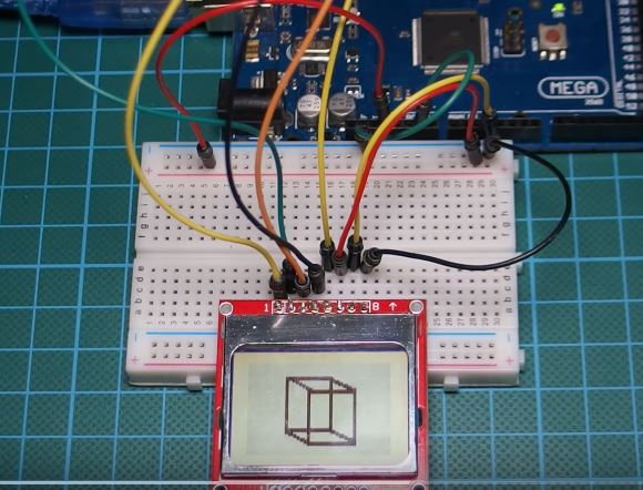
To interface with a micro controller and power itself, the display has two parallel 8-pin port to which headers pins can be connected. You can pick one of the sides and solder header pins to it for connection to the Arduino board.
There are two main power sources needed. The first one is the operational power supply which according to the data sheet should be between the range of 2.7V to 3.3V. The second power supply is required for the LCD back-light. The LCD circuit has no current limiting resistor inbuilt so its better to play safe and only power with 3.3V max.
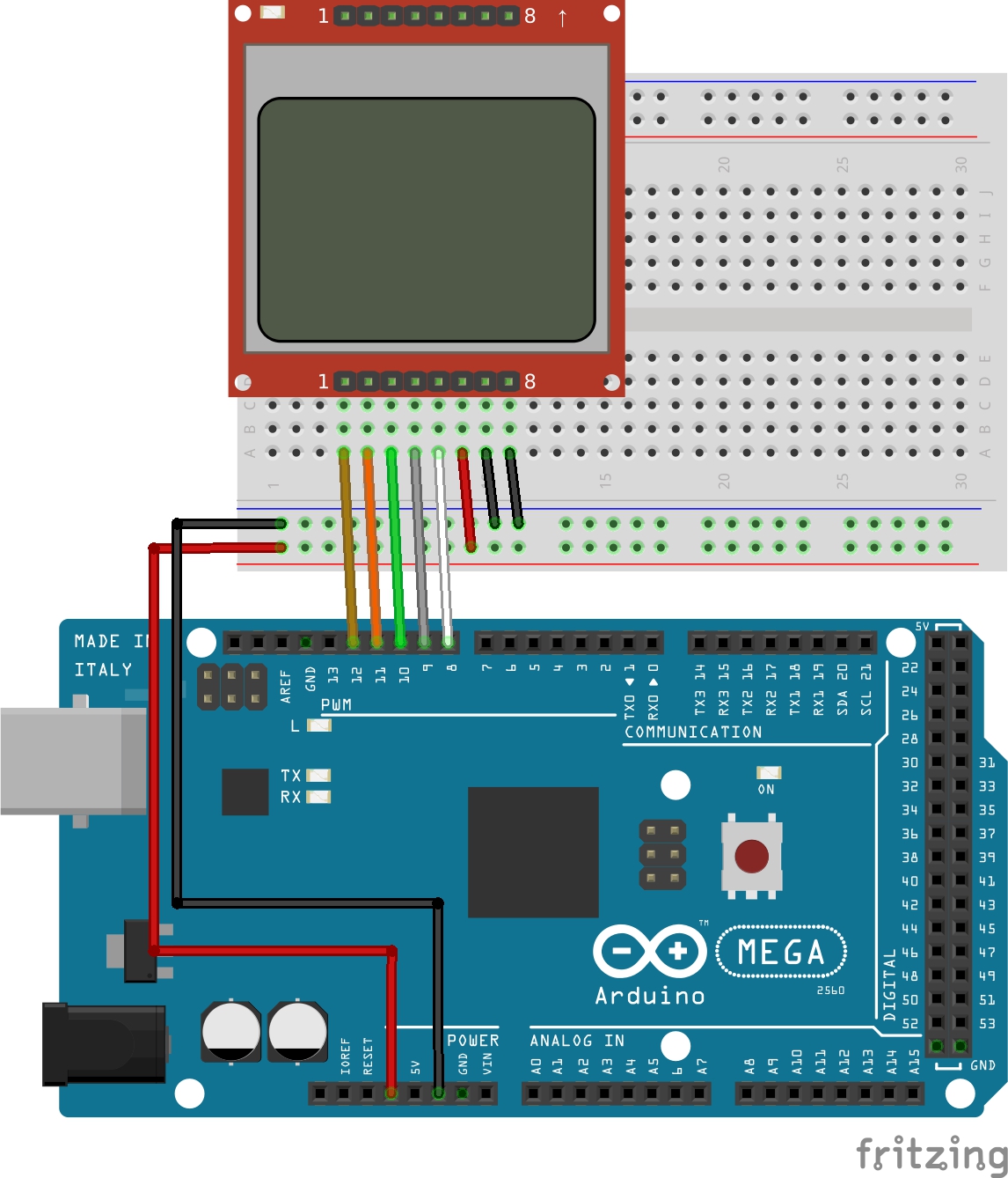
The LCD is connected to the Arduino as shown in the Schematics below.
After connecting the LCD to our Arduino, the next line of action is to prepare the graphics to be displayed.
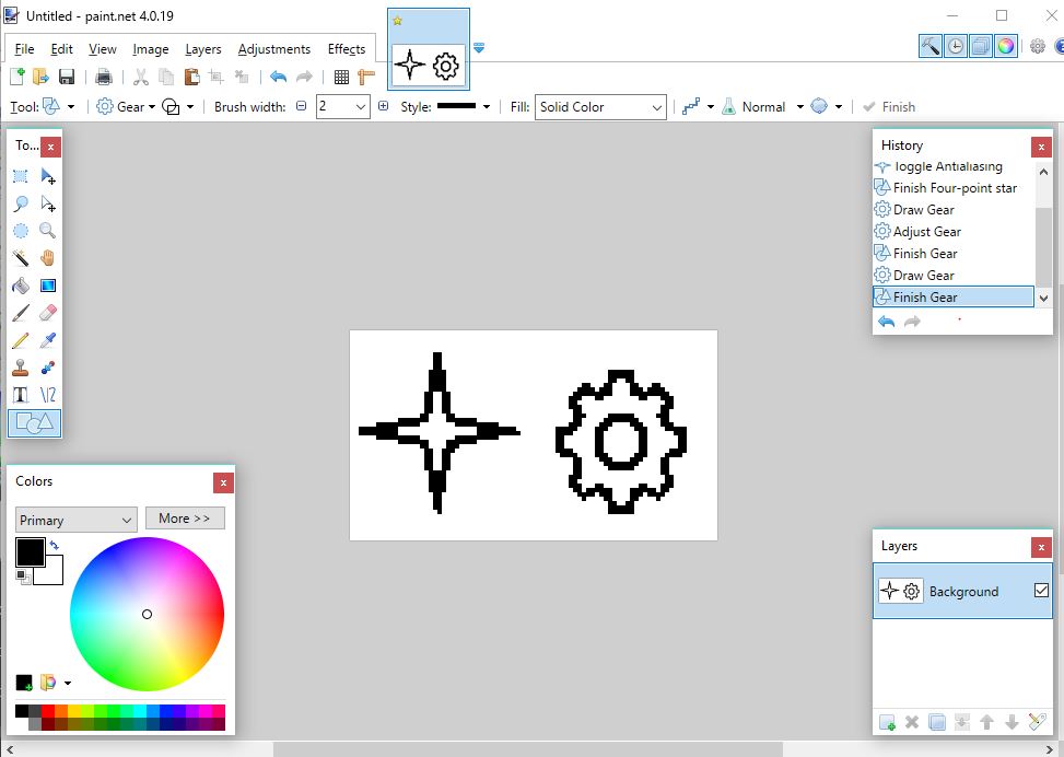
The graphics can be created using tools like, Microsoft paint, Corel draw, Paint.net or Adobe Photoshop. The important thing is to ensure the image is saved as a bitmap.
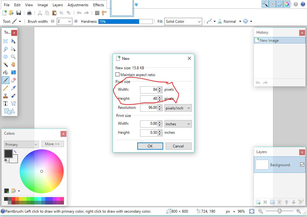
For the purpose of this tutorial, we will be using the paint.net tool to create the graphics. It is easy to use and can be downloaded from here. One thing that should be kept in mind while creating the graphics or logo is the canvass size. Since the LCD is 84×48, its important the canvass size is same as the screen, to ensure the designed graphics shows perfectly on the display.
Specify Canvas Size
Graphics design with paint.net
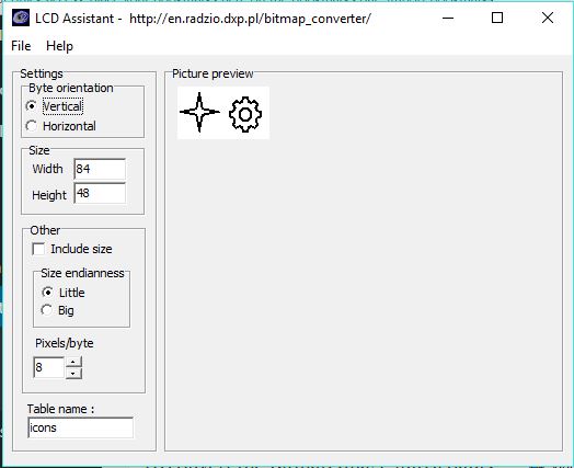
In order to load our own graphics into the Arduino to be displayed by the Nokia 5110 display, we will need to use the LCD assistant software. It is a free and easy to use software that converts bitmap images into a data array which can then be used in C programming language based firmware for any micro-controller. The software is available for download here.
To convert the Bitmap Image into a data array, the bitmap image is loaded into the LCD Assistant software.
Load bitmap into LCD Assistant
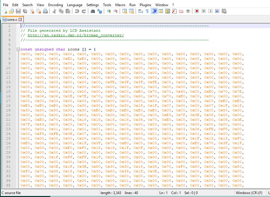
Then save output (Also found under file) as Graphics.c. The file can be previewed using a tool like notepad++ and your output should look something like the image below.
Output File (data array)
With this done, we are then ready to import the C file into our Arduino code.
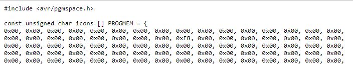
For better performance, we can save the data array in the program memory of the arduino instead of the sram, to save as much space as possible. To do this we will need to include some line of code to the data array file as shown in the image below.
Data array modified
The data array generated is attached in the zip file at the end of this tutorial.
Code
The Arduino code for this project is a fairly simple one, especially if you have checked out the previous tutorial on Nokia 5110 LCD Display Module.
The first thing we do is include the LCD5110 graph library by Henning Karlsen which can be downloaded here.
//Written by Nick Koumaris
//info@educ8s.tv
//educ8s.tv
#include <LCD5110_Graph.h>
After including the library, we then declare the pins on the Arduino to which the LCD is connected.
LCD5110 lcd(8,9,10,12,11);
Moving on, we declare the various graphics that will be used. For this example, we will be using three different graphics ( Icons, pi, cube) all loaded in the same Graphics.c file. Check the attached Graphics.c file attached at the end of the tutorial to see how they were merged.
We then move into the setup function and initialize the LCD.
void setup()
{
  lcd.InitLCD();
}
With the LCD initialized, we then move to the loop proper. For each of the graphics to be displayed, we first clear the screen using lcd.clrscr() and then draw the graphics using lcd.drawbitmap() with the coordinates, name of the file, and the size as parameters. update the display with lcd.update() and set a delay to give the graphics enough time to display on the screen.
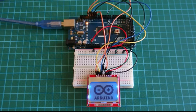
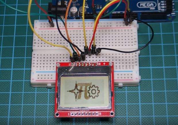
Copy the code, paste in the Arduino IDE, and upload to your Arduino board, you should get an output like the image below on your screen. Don’t forget to include the Graphics.c file in the Arduino sketch folder.
That’s it for this tutorial guys. As usual, let me know via the comment section, if you have any questions.
Happy holidays!
The youtube video of this tutorial is available here.
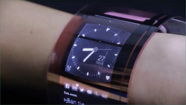
Nowadays, there is a lot of technology that implements wearables in fashion, medicine, worker safety, accessories and much more. Many wearables are coupled with uncomfortable charging cables that are irritating for users to handle, some even have big batteries that make wearables a burden instead of an advantage. Statistics show that people tend to abandon this devices after only 6 months of buying them, and battery life and portability is one of the issues. Addressing portability, the nanoengineers at the university of California San Diego have developed a new material that allows the creation of flexible, stretchable, and rechargeable batteries which can be printed into clothes.
This material named SIS can be expanded twice its size in any direction without any damage. SIS is made from a hyper elastic polymer material made from isoprene and polystyrene. The ink used to print the batteries is made with Zinc silver oxide with bismuth (to make it rechargeable). The whole flexible battery is made from both SIS and the ink. When zinc battery runs out, their electrodes react with the liquid electrolyte inside the battery which eventually shorts circuits the battery, bismuth prevents this from happening and ensures battery durability.
The prototype has 1/5 the capacity of a hearing aid rechargeable battery and it´s 1/10 as thick. It costs only $0.5 USD to produce and uses commercially available materials which makes it cheaper and smaller, but not as efficient as a common wearable battery. Two of these batteries are needed to power a 3 v LED, so a lot of them would be needed to power a bigger device.
The engineers are working towards improving performance to make them a good choice for wearable developers. They also want to extend their work towards lithium ion batteries, supercapacitor, and photovoltaic cells. Commercially, the short-term objective is to replace coin batteries for printable batteries which have a competitive price.
When performance is improved these batteries could power all kind of wearables for medical purposes such as shirts that can detects fever, or glucose sensor in diabetic patients. Also, for recreational purposes such as a sweatshirt with LEDs to run during night, or a shirts that detects movement and helps you with your movements while playing golf. Engineers for this project should consider implementing wireless charging to make it even more comfortable for the user by ending the need of cables and small connectors which are a nightmare for most of the people.
Pressure sensors are used today in many fields, such as automotive industry, touch screen devices, aviation and biomedical instrumentation, many of these applications require precise and accurate measures. Many times, this can not be achieved because of the limitations of the sensors such as the inability to measure on round surfaces (if they are twisted or wrinkled). To solve this problem a transparent and bendable nanofiber sensor was developed.
The sensor contains organic transistors and electronic switches which are made from carbon and oxygen based materials, this makes the sensor capable of bending over a radius of 80 millimeters, measuring in 144 locations simultaneously. It is only around 8 micrometers thick, and it’s not sensitive to distortion.
Additionally, the pressure sensor is transparent and small, so it can be incorporated in wearables and implants. Wearables have been developed to shorten hospitals visits, to keep track of chronic diseases and for older citizens who do not want to live in assisted living facilities. Wearable technologies are capable of sensing different parameters of various diseases and transfer the data to a health center or directly to the patient, so they can take actions regarding their health. This technology improves the life quality of many patients, and can stay on for really long periods of time. Also, the main objective of wearables is to go unnoticed by both the patient and other people which is why the developed pressure sensor needs to be capable of bending, and adapting to a person´s constant moves.
Many applications have arisen from this project. For example, this device could allow breast tumor detection avoiding uncomfortable mammographs, and invasive biopsies. Also, it can be used to detect pressure and speed of blood allowing easy and superficial examination and diagnosis. Woman could now be cancer tested from home, and people who suffer from cardiac or blood pressure diseases could now be monitored away from the hospital.
The flexible nanofiber was created by combining carbon nanotubes, graphene and elastic polymers which makes the sensor really accurate even when stretched and deformed. Many companies are developing sensors with the same capabilities, but this is the first one which is not sensitive to distortion. Even though the researchers are only looking toward improving biomedical industry, the applications for this pressure sensor could be expanded to many industries. There is still a long way to go to achieve this objective, but this sensor is the first step, and health industry its a great place to start.
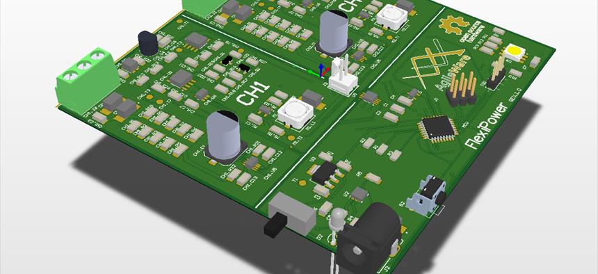
Hobbyists, makers, students and pretty much everyone who works with electronics has encountered the same issue, not having a handy power supply to test their projects. Usually, controllable power supplies are big, expensive and for some people difficult to access, and most small power supplies are not controllable. As a result, Roberto Lo Giacco created Flexipower, a small, portable, flexible, and remotely controllable dual channel power supply.
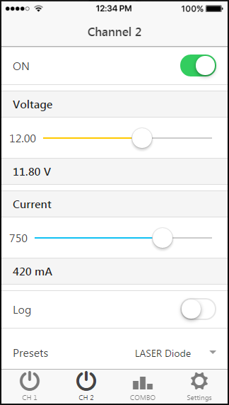
Flexipower is controlled via a mobile application and its battery operated. It can work up to a voltage of 20 V and a current of 1 A (per channel). Power supply is powered by two cell Li-Ion or Li-Poly batteries which provide 8.4 v when fully charged, to reach higher voltages the battery is fed into a voltage step up circuit, and to get lower voltages the battery is fed into a high current linear voltage regulator. Also, a simple voltage divider along with the 10-bit ADC is used to measure the produced voltage, and adjust accordingly.
Current measuring is done through a 1 Ohm shunt resistor network made by ten 10 Ohm resistors in parallel which results in 1 mV voltage drop per mA. In the case of currents lower than 320mA, the integrated circuit INA219 is used to obtain a very precise reading. When the supplied current goes above the capacity of the INA219 the shunt resistor voltage drop is measured using the 10 bit ADC.
As mentioned before, Flexipower uses 2 rechargeable batteries that are charged via a barrel jack connecting a 12 V source capable of around 1 A. An RGB LED is used to inform the user about the status of the device (power on, battery warning, connection status etc.). The LED is also used to indicate the battery status. Additionally, each channel has a green/red LED to indicate if it is enabled (green), or over current (yellow).
Furthermore, the device can create “Flexipower SSID”, an access point for people to connect and control the power supply. The app was created to avoid using a big LCD screen with limited data logging capabilities. The app allows control, unlimited data logging and visualization just with the use of a smartphone.
For complete specifications, list of materials used, schematics and app download go to official website. The creator always tried to minimize components costs while still providing a lot of capabilities. It still can be improved, but it’s a project that could make the life of people easier. Its important to clarify that this device is not a replacement for benchtop power supplies, but for portability is a great option.
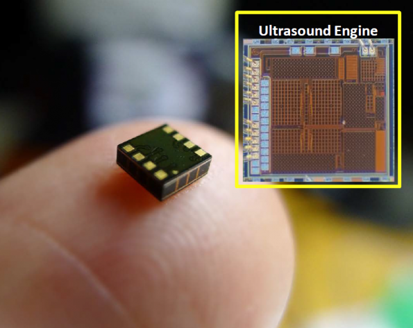
Recently Californian startup ChirpMicrosystemsofficially announced two discrete ultrasonic Time-of-Flight (ToF) sensors, the CH-101 and CH-201, with maximum sensing ranges of 1m and 5m, respectively. Both chips have a 3.5×3.5mm package and they are powered by same ASIC or application-specific integrated circuit for signal processing. To achieve different sensing ranges, the Piezoelectric Micro-machined Ultrasonic Transducers (PMUT), the MEMS parts of the sensors are tuned and built differently.
Chirp Microsystem designed smallest and most accurate ultrasonic Time-of-Flight sensors
Chirp Microsystems was founded in 2013 and the CH-101 is their 2nd generation design while the CH-201 is an upgraded third generation design. Their 4th generation design of chips is under development and prototypes are being tested recently. Chirp Microsystems declares that with each design so far, they’ve improved their transmitter and receiver performance by 4 times. David Horsley, Chirp Microsystems’ CTO, told,
In fact, we have been sampling the CH101 for two years now and we realized we had never made a product announcement for it.
According to Chirp Microsystems, the chips are the first commercially available MEMS-based ultrasonic ToF sensors and can beat all other ToF solutions on the small size and low power consumption. The “Sonars on a chip” draw 100 times less power and are a thousand times smaller than the conventional ultrasonic rangefinders used in today’s industrial automotive applications. Unlike infrared based ToF sensors, these new MEMS sensors do not rely on optical path clearance. So, it’s now easier for engineers to design bezel-free smartphones with precise gesture recognition.
The CH-101 and CH-201 include an interrupt pin and a GIO pin. That pin is used in hardware trigger mode to connect several transducers on the same I2C bus so they can operate in a synchronous fashion. For Virtual Reality applications, data from multiple chips are mixed to detect the position of user’s hand in 3D space.
Previously the California based startup also made monolithic linear arrays that had ten transducers in a row. Using that design, one can perform beamforming and identify both range and position of an object. Though they stayed away from commercializing it. “We didn’t want to bite too much at a time” – said the CTO of the startup. Rather they decided to focus on solving various manufacturing and packaging issues first. Horsley, the CTO of the Chirp Microsystems, also added,
We are pioneers in this area, and we are not close to the optimum yet, we still have a lot of design space to improve the specs.
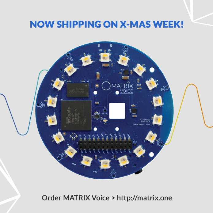
MATRIX Voice is a”Voice Recognition” development board, designed for the Raspberry Pi or Stand-alone with ESP32 (WiFi/BT/MCU)
MATRIX Voice is an open-source VOICE RECOGNITION platform consisting of a 3.14-inches in diameter dev board, with a radial array of 7 MEMS microphones connected to a Xilinx Spartan6 FPGA & 64 Mbit SDRAM with 18 RGBW LED’s & 64 GPIO pins. Providing developers the opportunity to integrate custom voice & hardware-accelerated machine learning technology right onto the silicon. An ESP32 Wi-Fi / BT enabled 32 bit microcontroller version is available. It’s for makers, industrial and home IoT engineers.
The project is already funded on indiegogo.com and shipping begins next week.
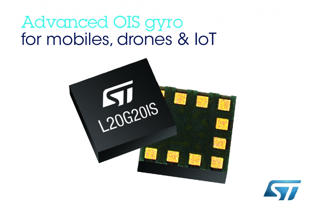
STMelectronics introduces a super tiny two-axis gyroscope (L20G20IS), a Micro-Electro-Mechanical system (MEMS) designed for the optical image stabilization for Smartphones with less energy consumption compared to its predecessor (L2G2IS).
A gyroscope, or gyro for short, adds an additional dimension to the information supplied from the accelerometer by tracking rotation or twist. An accelerometer measures linear acceleration of movement, while a gyro on the other hand measures the angular rotational velocity.
The gyro and the accelerometer work together to detect the rotation of phone and other features like tilting of phone while playing racing games, enhancing the overall gaming experience or in this case, achieving optical image stabilization.
The L20G20IS ultra-compact square gyro uses 25% less surface to shrink camera module size, simplify circuit design and allowing development of thinner devices. The gyro fixes the thin substrates deformations resulted by smartphone moves to ensure consistent measurements for image stabilization.
Features:
±100 dps / ±200 dps full-scale range
5 degree phase delay · 3.8 mdps/√(Hz) rate noise density
Wide supply voltage range: 1.7 V to 3.6 V
Low-voltage compatible IOs
3- and 4-wire SPI digital interface
Embedded temperature sensor
Embedded self-test
Integrated low-pass filters with user-selectable bandwidth
Power-down and sleep modes for smart power saving
ECOPACK®, RoHS and “Green” compliant
Volume (2.0 x 2.0 x 0.7)mm
Zero-rate Level: 0.03dps/°C (range: -20°C to 75°C)
Also L20G20IS includes a sensing element and an IC interface capable of providing the measured angular rate to the application through an SPI digital interface. It is compatible with single- or dual-camera modules and is available now in the 12-lead 2mm x 2mm LGA package.
Zero-rate level: This value indicates “the deviation of an actual output signal from the ideal output signal if no acceleration is present”, or more clearly the output value that will be generated when there is no movement on the device. This is very important for the phone, it needs to know when it is not moving to be able to stabilize the images with the appropriate values.
Results
Smaller but more efficient gyroscope! The L20G20IS boots 30% faster (in less than 70ms) consuming just 1.4mA (50% less of current than usually). Although, the temperature can affect the sensitivity and the zero-rate level of the gyro, producing wrong measurements for image stabilization by the phone. However, the L20G20IS device has a integrated temperature sensor to guarantee sharper images to the users even with long exposure times.
The smart-camera software saves even more battery with the power-down and sleep modes. Another improve is the suppression ratio of 6dB, it gives outstanding optical correction to banish camera shake from smartphone photography.
Source: Micro-Electro-Mechanical Systems (MEMS). ST is a world leader in MEMS devices for mobile applications, with more than 900 MEMS-related patents and patent applications worldwide.
The transistor revolutionized the field of electronics, and paved the way for smaller and cheaper radios, calculators, and computers, among other things since its very first practically implemented device as a point-contact-transistor invented in 1947 and getting the Nobel Prize in Physics in 1956.
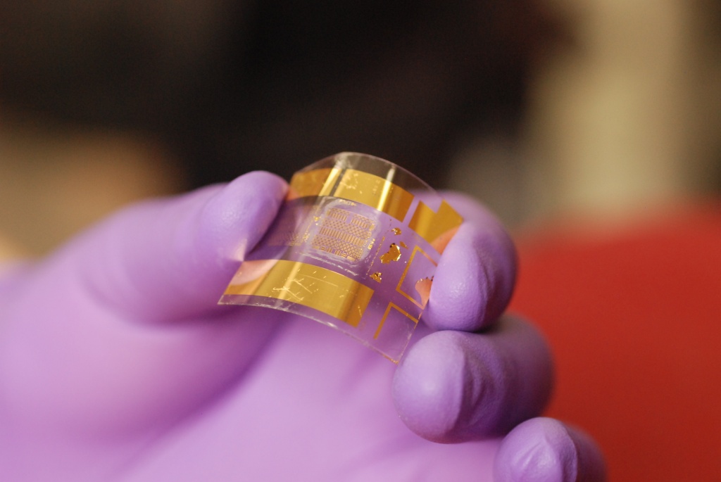
Now, engineers from the University of Wisconsin-Madison (UW-Madison) have built the most flexible, fully-functional transistor in the world! The BiCMOS (Bipolar Complementary Metal Oxide Semiconductor) thin-film transistor has all current transistor’s characteristics: speed, carrying large current and low dissipation – but it is extremely flexible.
This is an interesting advance that could open the door to an increasingly interconnected world, enabling manufacturers to add smart wireless capabilities to any number of large or small products that curve, bend, stretch and move.
Making traditional BiCMOS flexible electronics was difficult, in part because the process takes several months and requires a multitude of delicate, high-temperature steps. Even a minor variation in temperature at any point could ruin all of the previous steps. This fabrication process is not currently as commercially viable for most of applications.
However, the engineers fabricated their flexible electronics on a single-crystal silicon nanomembrane on a single bendable piece of plastic. The secret to their success is their unique process, which eliminates many steps and slashes both the time and cost of fabricating the transistors.
This new electronic has the potential to change the electronic’s industry in a new way. Everything touched by electronics (computers, microcontrollers, sensors…) could be completely flexible due the easily of this new technology to scale up to commercial levels.
The vast majority of transistors are now produced in integrated circuits. A logic gate consists of up to about twenty transistors whereas an advanced microprocessor, as of 2009 and with a cost of just a couple of usd, can use as many as 3 billion transistors. This is the best transistor’s advantage: mass-production with a extremely low cost.
For that reason, the transistor is the key active component in practically all modern electronics. The transistor is on the list of IEEE milestones and many consider it to be one of the greatest inventions of the 20th century.
This new flexible transistor could be in future electronic boards for a flexible electronics development and applications never even seen before. Definitely, the future is now.
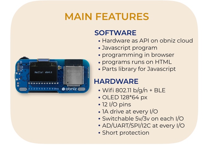
Obniz is the world’s first development board which IO is available as API on the cloud. It’s Tiny but powerful, Internet connected board.
obniz has 12 IO and WiFi module and It can be controlled through the APIs on obniz cloud, either through the REST or WebSocket API. The API can be used in javascript, so obniz programs written in JavaScript can run on a webpage, so “Turning on a motor by pressing a button on the Web” is an easy task!
With obniz, it’s easy to make any hardware project you can think of! Just connect motors or sensors to an obniz then program it via the Internet. No App or firmware flashing is required. Program it from your PC or smartphone now!