Researchers Develop Long Range Backscatter Sensors That Consume Almost No Power

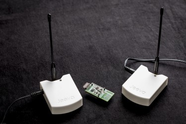
Researchers at the University of Washington developed a new backscatter sensors that can operate over long ranges with very little power. The researchers demonstrated for the first time that the device runs on almost zero power and can transmit data across distances of up to 2.8 kilometers.

The long-range backscatter system developed by UW researchers

Backscatter communication works by emitting a radio signal and then monitoring the reflections of that signal from sensors. As the transmitter generates the signal, the sensors themselves require very little power. But this kind of system badly suffers from noise. Noise can be added anywhere – on the transmitter side, on the channel or on the sensor array. The key to solving this problem is a new type of signal modulation called chirp spread spectrum.

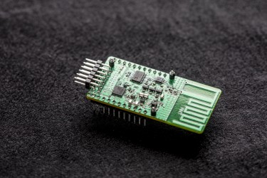
By using the chirp spread spectrum modulation technique, the team was able to transmit data up to 2.8 kilometers while the sensors themselves consumed only a few microwatts of power. Such extremely low power consumption lets them run by harvested ambient energy and very small printed batteries. The cost is surprisingly cheap too. The sensors would cost just 10 to 20 cents per unit if bulk purchased.

Today’s flexible electronics and other sensors need to operate with very low power typically can’t communicate with other devices more than a few feet or meters away. By contrast, the University of Washinton’s long-range backscatter system achieved pretty strong coverage throughout a 4800-square-foot house, an office area including 41 rooms, and a one-acre vegetable farm at extremely low power and low cost.

Shyam Gollakota, the lead faculty and associate professor in the Paul G. Allen School of Computer Science & Engineering, said,

Until now, devices that can communicate over long distances have consumed a lot of power. The tradeoff in a low-power device that consumes microwatts of power is that its communication range is short. Now we’ve shown that we can offer both, which will be pretty game-changing for a lot of different industries and applications.

These low-power sensors have endless potential applications. They can be used for everything from wearable health monitors to scientific data collection devices. Though there are no confirmed products yet, the team has created few prototypes in the form of flexible sensors worn on the skin, smart contact lenses, and more.

2.9″ ESPaper Lite Kit for $39.90

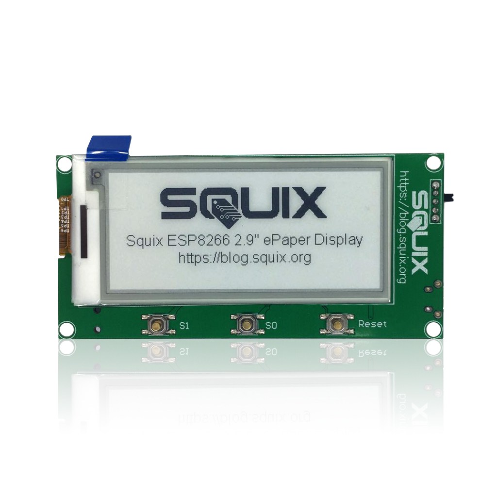
The 2.9″ ESPaper Lite Kit contains most of the parts you need to display data over wifi:

With the 2.9″ ESPaper module you can display data retrieved over WiFi on an ePaper with little effort. The integrated ESP8266 Wroom-02 module updates the 296×128 B&W ePaper display over the SPI bus. The module also features a charging circuit for LiPo batteries and a JST connector which allows you to run the module for weeks or even months from a battery. How long the module can be run from battery mostly depends on the update frequency and the battery capacity. In tests we could run the module from a 800mAh LiPo battery for several weeks by updating weather information every 20 minutes.

2.9″ ESPaper Lite Kit for $39.90 – [Link]

Teardown & Repair of an Agilent N1912A P-Series Power Meter

In this episode Shahriar investigates a peculiar problem with an Agilent P-Series Power Meter. While the instruments works during startup, after about 10 minutes the LCD screen begins to flicker and become scrambled. Initial investigation reveals that the issue is not likely with the main motherboard since USB connection to the instrument and data-readout is possible even when the LCD screen is malfunctioning.

Teardown & Repair of an Agilent N1912A P-Series Power Meter – [Link]

FemtoUSB Board (Atmel ARM Cortex M0+)

Arduino compatible, Atmel SAM D21 chip, open source!

This is one of the smallest ARM powered boards in the world. If you are ready to transition away from AVR 8-bit hardware to the very powerful ARM 32-bit stuff, this is the way to learn! The board design, schematic, and parts lists are completely open-source.

FemtoUSB Board (Atmel ARM Cortex M0+) – [Link]

Dremel Introduces The First-Ever Dremel Digilab Laser Cutter

The Dremel Laser Cutter backed by 85 years of the Dremel brand legacy, will provide a higher level of safety, ease, reliability and quality to users. (PRNewsfoto/Dremel)

The Dremel DigiLab Laser Cutter enables Makers to expand portfolio and business capabilitie.

MOUNT PROSPECT, Ill., Sept. 23, 2017 /PRNewswire/ — At World Maker Faire New York, Dremel introduces the first-of-its-kind Dremel DigiLab Laser Cutter. Dremel designed this machine to provide Makers of all levels and practices with an outlet for innovation. As the brand’s latest addition to its lineup of digital fabrication tools, it has the ability to customize a variety of materials quicker and easier than ever before.

The Dremel Laser Cutter backed by 85 years of the Dremel brand legacy, will provide a higher level of safety, ease, reliability and quality to users. This tool can cleanly slice through tougher materials like wood, acrylic, leather and paper as well as neatly engrave tougher surfaces such as glass and anodized metal. Dremel President John Kavanagh shared how the new Dremel Laser Cutter will enhance the productivity of Makers and industrial professionals across a broad spectrum of applications.

The new Dremel Laser Cutter allows a level of precision you just can’t get by hand because it is so detailed,” Kavanagh said. “It is truly designed and built for business owners to personalize any project and improve efficiency. With a higher level of reliability and ease of use, the Dremel DigiLab Laser Cutter eliminates many of the repetitive, laborious steps and allows Makers to create new projects they couldn’t necessarily do before.

iEAT – A Powerful Keychain Detector To Detect Food Allergens

For kids and adults with food allergies, having meals from restaurants or hotels can sometimes be very risky. Even when ultimate care is taken, freshly prepared meals can accidentally become cross-contaminated with an offending food and trigger an allergic reaction. Every year many people end up in the emergency room due to food allergies. Researchers of the Harvard Medical School developed an affordable device called iEAT for detecting allergens, which can reduce the anxiety of the people prone to allergies.

iEAT - A Portable allergen-detection system
iEAT – A Portable allergen-detection system

Conventional methods to detect the hidden allergens require massive laboratory equipment. They are slow and also do not work on a low concentration of allergens. Ralph Weissleder, Hakho Lee, and their colleagues at the Harvard Medical School wanted to make a more practical, consumer-friendly alternative. They reported in the journal ACS Nano the development of a new portable allergen-detection system that features a keychain analyzer for detecting allergens in food anywhere, anytime.

The portable allergen-detection system called integrated exogenous antigen testing or iEAT is small enough to fit in your pocket and it costs $40 only. The iEAT consists of a handheld device to extract allergens from food and an electronic keychain reader for sensing allergens. Then, the result is wirelessly sent to a smartphone. The prototype is able to detect five allergens within 10 minutes, one each from wheat, peanuts, hazelnuts, milk, and egg whites, even if they are in very low concentration.

The main device uses a disposable sample collector which is inserted into the small-sized main unit. The device is so sensitive that the scientists were able to detect gluten in foods advertised as being “gluten-free”. For example, the device detected gluten in salad and an egg protein in beer. Although the prototype was primarily designed to sense five allergens only, the researchers say the device could be expanded to test for many additional compounds, including other allergens and non-food contaminants such as pesticides.

3A Thermoelectric Cooler (TEC) Driver

3A TEC Driver Module is a complete power stage solution to drive Thermoelectric Cooler (TEC). The required DC voltage input controls the output current. It consists of the Texas instruments DRV593 power driver IC, along with a few discrete passive components required for operation. It also includes jumpers for configuring the features of the device, LEDs for fault monitoring, and an output filter. The 4 Pin header connector  for the inputs, 4 pin header connector for  output, and 4 Pin header connector for power supply, provide ease of connection to any system, from an existing design to a bread-boarded prototype. Connect a dc control voltage to CN1 Pin 3 (IN+), ranging from ground to VCC. The Pin 7 of the IC is held to VCC/2 with a resistor voltage divider, as shown in the schematic. Therefore, a dc control voltage of VCC/2 provides 0-V output from PWM to H/C. Input DC voltage range is 1.2V to 3.8V when supply voltage is 5V and 1.2V to 2.1V when supply voltage is 3.3V.

Features

  • 3A Maximum Output Current
  • Low Supply Voltage 2.8V To 5.5V
  • Frequency 500 KHz (Refer to Note To change Frequency)
  • High Efficiency Generates Less Heat
  • Over Current and Thermal Protection
  • Fault LED for Over Current, Thermal & Under Voltage Conditions
  • When J3-Jumper is closed, the board is configured for 500-kHz operation.

3A Thermoelectric Cooler (TEC) Driver – [Link]

3A Thermoelectric Cooler (TEC) Driver

3A TEC Driver Module is a complete power stage solution to drive Thermoelectric Cooler (TEC). The required DC voltage input controls the output current. It consists of the Texas instruments DRV593 power driver IC, along with a few discrete passive components required for operation. It also includes jumpers for configuring the features of the device, LEDs for fault monitoring, and an output filter. The 4 Pin header connector for the inputs, 4-pin header connector for output, and 4 Pin header connector for the power supply provide ease of connection to any system, from an existing design to a bread-boarded prototype. Connect a dc control voltage to CN1 Pin 3 (IN+), ranging from ground to VCC. The Pin 7 of the IC is held to VCC/2 with a resistor voltage divider, as shown in the schematic. Therefore, a dc control voltage of VCC/2 provides 0-V output from PWM to H/C. Input DC voltage range is 1.2V to 3.8V when the supply voltage is 5V and 1.2V to 2.1V when the supply voltage is 3.3V.

The DRV593 is a high-efficiency, high-current power amplifier ideal for driving various thermoelectric cooler elements in systems powered with 2.8V to 5.5V. The operation of the device requires only one inductor and capacitor for the output filter, saving significant printed-circuit-board area. Pulse width modulation (PWM) operation and low output stage on-resistance significantly decrease power dissipation in the amplifier. The IC is internally protected against thermal and current overloads. Logic level fault indicators signal when the junction temperature has reached approximately 128 degrees centigrade to allow system level shutdown before the amplifier’s internal thermal shutdown circuitry activates. The fault indicators also signal when an over-current circuitry is tripped, and the devices automatically reset. The PWM switching frequency has been set to 500 KHz, this can be changed to 100 KHz by changing capacitor value C2 1nF. The amplifier’s gain is at 2.3V/V.

Note: This board requires DC input voltage to control the TEC temperature, 1.2 V to 3.8 V when using a 5-V supply, and 1.2 V to 2.1 V when using a 3.3-V supply.
When J3 Jumper is Open, the device is configured for 100kHz operation. However, capacitor C2 must be removed and replaced with a 1nF capacitor for proper operation.

Features

  • 3A Maximum Output Current
  • Low Supply Voltage 2.8V To 5.5V
  • Frequency 500 KHz (Refer to Note To change Frequency)
  • High Efficiency Generates Less Heat
  • Over Current and Thermal Protection
  • Fault LED for Over Current, Thermal & Under Voltage Conditions
  • When J3-Jumper is closed, the board is configured for 500-kHz operation.

Connections

  • J2-Jumper closed for normal operation
  • J1-Jumper closed for normal operation when the jumper is open device goes into shutdown mode
  • The common mode input range is 1.2 V to 3.8 V when using a 5-V supply, and 1.2 V to 2.1 V when using a 3.3-V supply

Schematic

Parts List

Connections

Fault Table

Photos

DRV593 Datasheet

Tyre pressure monitoring system using Bluetooth Low Energy

Author: Maurizio Di Paolo Emilio

A tyre pressure monitoring system (TPMS) aims to monitor air pressure on various automotive systems. The most common TPMS sensors mainly use sub-GHz radio standards to transfer information to the vehicle’s computer. There are two different types: direct (dTPMS) and indirect (iTPMS). The use of bluetooth low energy (BLE) connectivity makes it possible offering a high performance. All information will be displayed in real-time by simple user interface with low power consumption. With low power consumption, applications can run on a small battery for many years. As result, it’s actually extremely positive when talking about M2M communication and automotive systems.

TPMS helps to avoid the tyre wear and improves road safety.  Due to the advantages of a longer battery life and connectivity, DA14585 is suitable for IoT applications in various industries. The figure 1 show a typical block diagram for a TPMS system.

block diagram of TMPS general system
Figure 1: block diagram of a TPMS. The block of transmission (transmit data) can implement the bluetooth low energy protocol.

Bluetooth low energy for automotive industry

Connectivity, Intelligence and energy saving are the main features for the new generation of IoT devices. Luckily, SmartBond can achieve all these features. Especially relevant is one of the series, DA14585 SoC. It offers all benefits, such as, full support of all bluetooth standards, including version 5. Moreover, it is suitable  for many applications, as remote controls, proximity tags, headlights, connected medical devices, smart home and smart automotive (Figure 2). The figure 2 shown the block diagram of DA14585, where is visualized the ARM M0 core and other peripherals.

block diagramm of DA14585 for bluetooth low energy applications
Figure 2: block diagramm of DA14585

With 96 kB of RAM and retention capability, DA14585 offers a wider memory than its predecessor in order to fully utilize standard features. Moreover, it also includes an integrated microphone interface for low-cost voice support. DA1485 supports a wide range of power supply voltages from 0.9 to 3.6 V. This range offers a wider choice of energy sources with a great design performance.

As a result, DA14585 represents the ideal solution to add bluetooth low energy technology to various applications. It supports Data Packet Length Extension, Link Layer Privacy v1.2, Secure Connections, Bluetooth Low Power Mesh and Efficient Connectable Advertising. Dialog Semiconductor has started contacting with the automotive industry for the construction of first TPMS devices with BLE. The goal is to manage the entire measurement process with the addition of sensors for measuring temperature and pressure. All powered by a simple battery.

The initial adoption of BLE technology for TPMS is a great opportunity for the automotive market and for new TPMS devices. As a result, the advent of BLE connectivity in automotive systems will open many connectivity scenarios for the smart automotive market.

LT8362 – Low IQ Boost/SEPIC/Inverting Converter with 2A, 60V Switch

The LT8362 is a current mode, 2MHz step-up DC/DC converter with an internal 2A, 60V switch. It operates from an input voltage range of 2.8V to 60V, suitable for applications with input sources ranging from a single-cell Li-Ion battery to automotive and industrial inputs. The LT8362 can be configured as either a boost, SEPIC or an inverting converter. Its switching frequency can be programmed between 300kHz and 2MHz, enabling designers to minimize external component sizes and avoid critical frequency bands, such as AM radio. Furthermore, it offers over 90% efficiency while switching at 2MHz. Burst Mode operation reduces quiescent current to only 9μA while keeping output ripple below 15mVP-P. The combination of a 3mm x 3mm DFN or high voltage MSOP-16E package and tiny externals ensures a highly compact footprint while minimizing solution cost.

LT8362 – Low IQ Boost/SEPIC/Inverting Converter with 2A, 60V Switch – [Link]

TOP PCB Companies