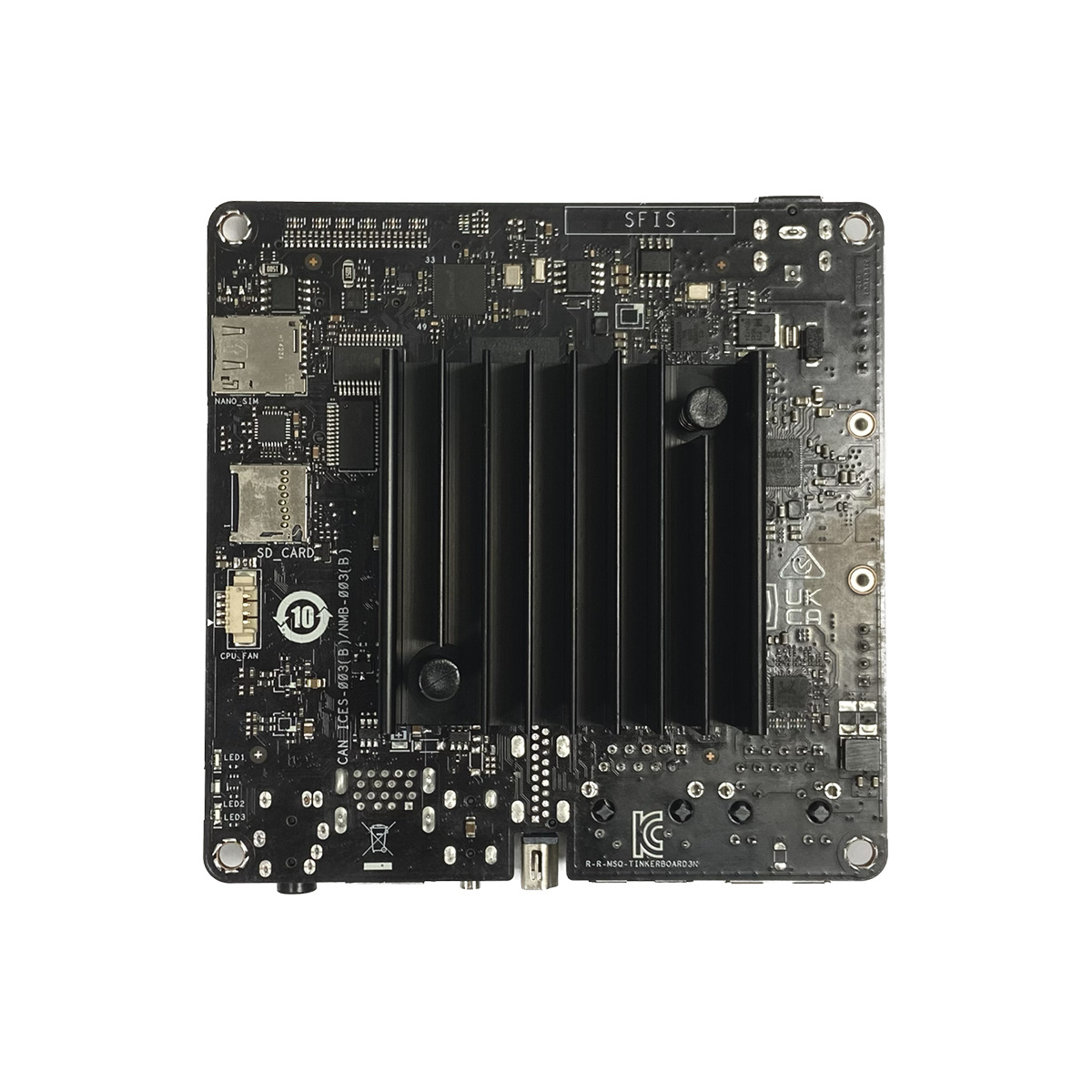
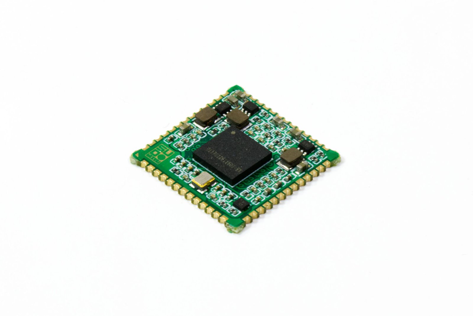
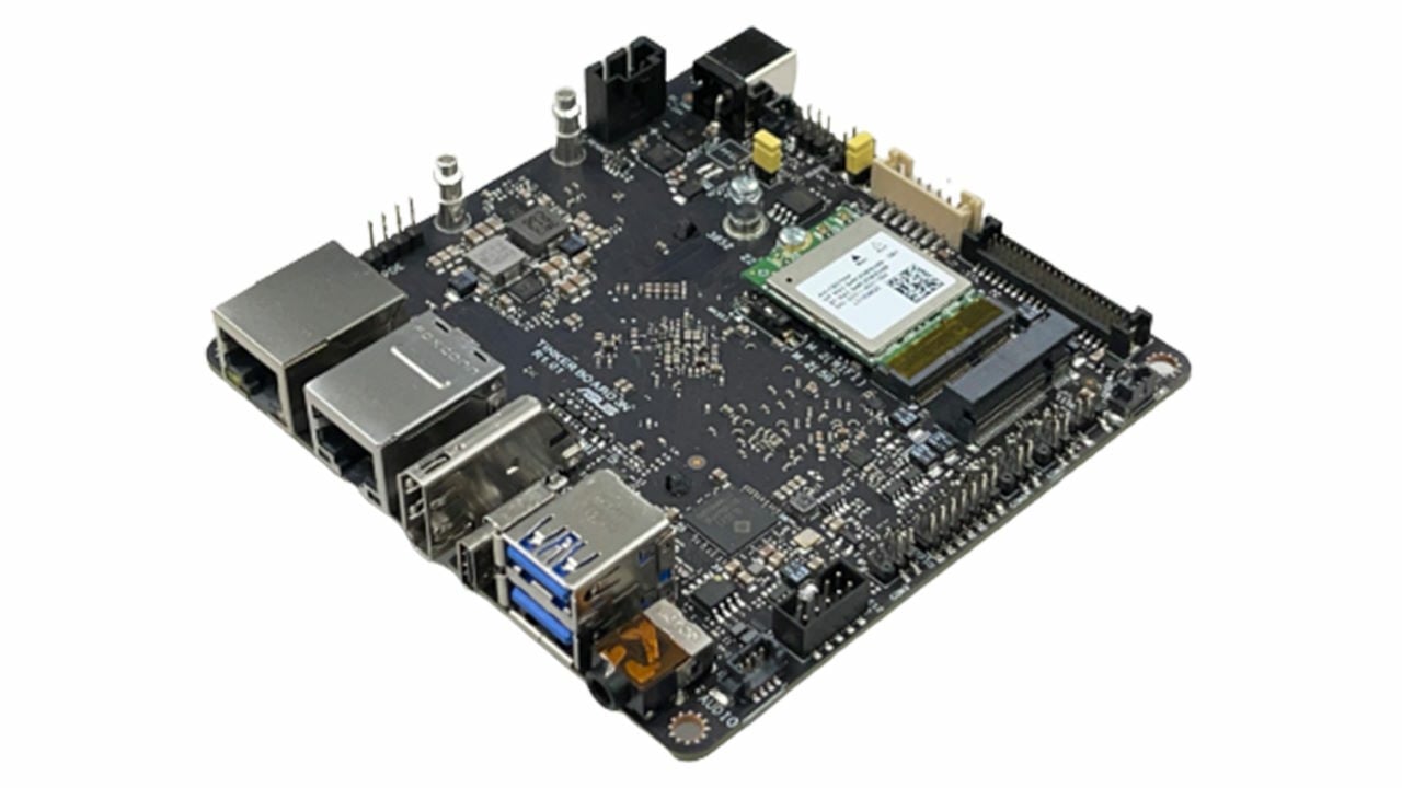
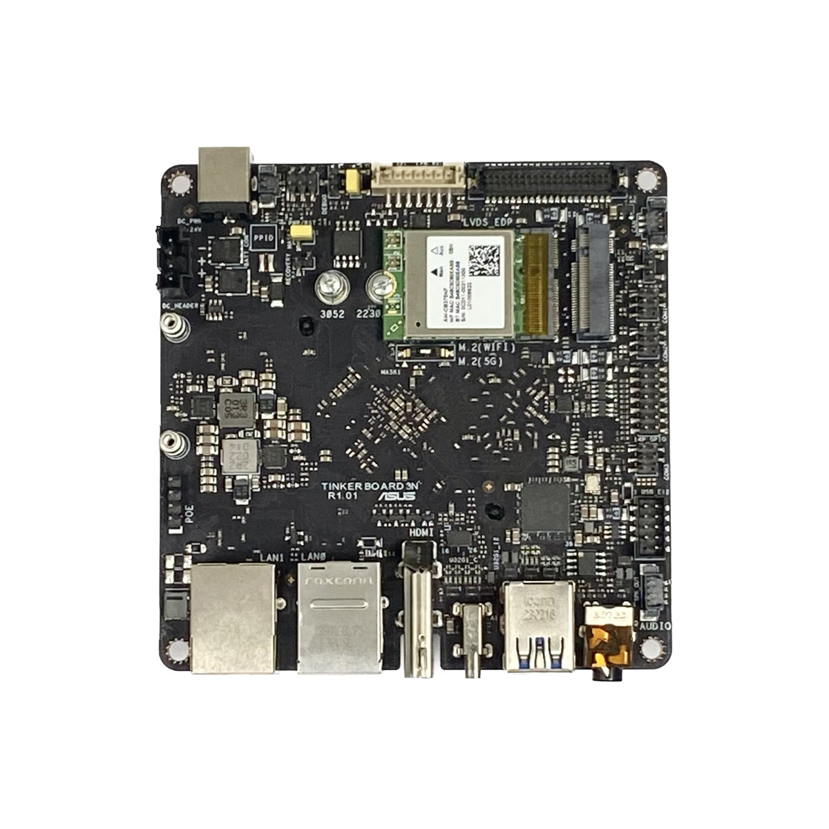
ASUS IoT has announced Tinker Board 3N series, a versatile, Arm-based single-board computer (SBC) that empowers easy system integration, broad adaptability and expandability.
The NUC-sized SBC series is equipped with rich I/O and supports Linux Debian, Yocto, and Android operating systems, presenting an all-new premium option for developers and system integrators’ diverse IIoT projects. Its optimised thermal design simplifies the deployment of embedded applications, ensuring efficient operation in demanding environments.
With its durable and reliable design, Tinker Board 3N offers enhanced computing performance, low power consumption and a wide range of interfaces, so it’s primed and ready for smart manufacturing applications powering the IoT revolution.
Versatile performance and advanced graphics processing
To deliver the raw power and versatility demanded by IIoT applications, Tinker Board 3N is equipped with a 64-bit, quad-core Arm Rockchip RK3568 processor. Built on the Arm v8 architecture, this generates remarkable GPU performance for seamless graphics processing with low power consumption. Exacting in-house tests show that Tinker Board 3N delivers up to 17%-higher GPU performance and up to 31% increase in total UX score, encompassing data security, processing capabilities and image and video processing, Tinker Board 3N excels in IoT gateway, human-machine interfacing (HMI), and factory automation.
Robust and resilient thermal design
In addition to its outstanding computing performance, Tinker Board 3N incorporates several mechanical design enhancements to facilitate embedded application use with flexibility. For example, it features a low-profile pushpin heatsink and SoC placement on the back side for added strength and ease of installation, with its diminutive NUC-scale dimensions allowing for SWaP-constrained space deployment and flexible system integration. It is also engineered to operate smoothly in harsh industrial environments, with an impressive operating-temperature range of -40 to 85°C in order to fulfill industrial automation needs.
Enhanced connectivity for diverse applications
Tinker Board 3N-series devices are equipped with PoE, LVDS, COM, and CAN bus interfaces, along with M.2 E and M.2 B slots to accommodate WiFi 5/6 and 4G/5G expansion modules for cloud computing. The onboard LVDS supports FHD output via dual channels, making it suitable for multiple display solutions, while embedded COM headers and CAN bus can be utilized in diverse applications, such as controllers and robotic arms, expanding the board’s usability. Delivering enhanced computing performance, remarkable expandability and cost-effectiveness, Tinker Board 3N series is perfectly suited for industrial automation and smart factory environments. It fulfills the need for real-time communication, frictionless integration, long-term operation, and stringent revision control, making it an ideal choice for fulfilling the demands of versatile applications in these settings.
Support for the latest operating systems
Tinker Board 3N supports a variety of the latest and mainstream operating system platforms, catering to different development environment needs. Users can choose from Linux Debian, Yocto, and Android operating systems. The latest ASUS IoT SBC supports firmware over the air (FOTA) for both Android and Linux, ensuring regular software updates and system maintenance for efficient and optimal performance.
Tinker Board 3N is available in three distinct flavors to meet diverse project requirements. These include Tinker Board 3N PLUS, Tinker Board 3N and Tinker Board 3N LITE.
Offered in Compact 1.85 mm by 1.2 mm by 0.6 mm SMD Package, Device Features CTR of 31 %, Sensing Distance of 15 mm, and Lower Power Consumption.
The Optoelectronics group of Vishay Intertechnology, Inc. today introduced a new reflective optical sensor for industrial, computer, consumer, and mobility applications. Saving space compared to previous-generation solutions — while delivering improved performance with a higher current transfer ratio (CTR), increased sensing distance, and lower power consumption — the Vishay Semiconductors VCNT2030 features a vertical-cavity surface-emitting laser (VCSEL) and a silicon phototransistor in a miniature 1.85 mm by 1.2 mm by 0.6 mm surface-mount package.
The device released today features a compact construction in which the emitting light source and detector are arranged in the same plane. It offers excellent internal crosstalk suppression due to the VCSEL’s narrow ± 17°emission angle, which also enables improved proximity performance behind cover glass. The VCNT2030’s analog output signal at the phototransistor is dependent on the amount of light emitted by the VCSEL and reflected off an object in the sensor’s field of view. The device offers a sensing distance of 15 mm, which is three times higher than the closest competing device on the market.
With its compact footprint, the VCNT2030 saves > 40 % PCB space compared to previous-generation devices, allowing the sensor to serve as a space-saving solution for optical switching in industrial infrastructure, home and building controls, notebook and desktop computers, home appliances, consumer electronics, and metering applications; optical encoding for motor control in e-bikes, golf carts, tractors, and harvesters; and paper presence detection in printers and scanners. In these applications the low 8 mA driving current of the device’s VCSEL is enough to achieve the same performance as solutions using 20 mA infrared emitters, dramatically lowering power consumption.
The sensor offers a detection range of 0.3 mm to 6 mm, an emitter wavelength of 940 nm, and a typical output current of 2.5 mA, which represents a typical CTR of 31 % under test conditions. This value is > 100 % higher than previous-generation solutions and the closest competing sensor. The device features a Moisture Sensitivity Level (MSL) of 3 for reflow soldering according to J-STD-020. It is RoHS-compliant, halogen-free, and Vishay Green.
Samples and production quantities of the VCNT2030 are available now, with lead times of eight to 16 weeks.
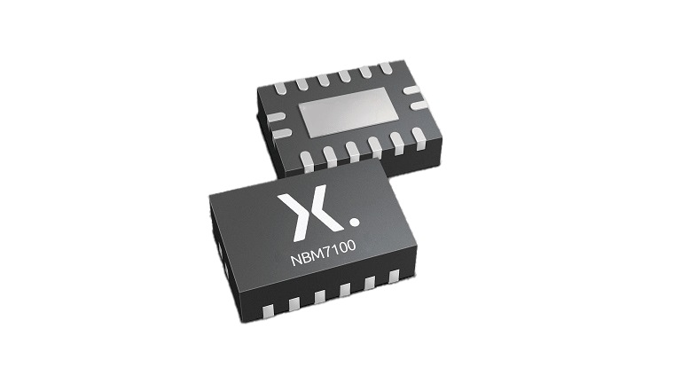
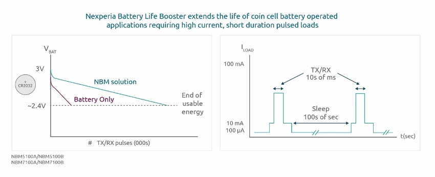
The NBM7100 and NBM5100, are revolutionary new types of battery life boosting ICs designed to extend the life of a typical non-rechargeable lithium coin cell battery by up to 10x compared to competing solutions while also increasing its peak output current capability by up to 25x compared to what a typical coin cell can deliver without a battery booster. This unrivaled extension in working life will significantly reduce the amount of battery waste in low-power Internet of Things (IoT) and other portable applications while making coin cells a viable power source for applications that could previously only operate from AA- or AAA- batteries.
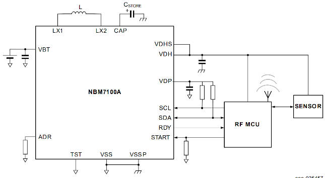
The NBM7100A/B contains two stages of high-efficiency DC-DC conversion and an intelligent learning algorithm. The first stage DC-DC conversion transfers energy from the lithium battery at a low constant current to a capacitive storage element. Once charged, a second DC-DC conversion cycle utilizes this stored energy to supply a regulated voltage with high pulse load current capability on the VDH output pin. The battery is never directly subjected to large load pulse currents, resulting in a longer, more predictable battery lifetime.
Key features
Extends useful battery life of coin cell-powered IoT devices
Regulated output voltage powers RF circuits requiring high pulse current
Low standby current minimizes battery drain
Protection against battery voltage dips (brown-out)
Additional features
Programmable constant battery load current: 2 to 16 mA
Protection against battery voltage dips (Brown-out)
Pulse load output current: ≤ 200 mA
Regulated programmable output voltage VDH: 1.8 V to 3.6 V
Ultra-low standby current: < 50 nA
Typical conversion efficiency of > 90% with adaptive optimization
63 adaptive load optimization settings
Integrated fuel gauge
Small 16 pin lead-free package (SOT763-1/DHVQFN16; 2.5 mm × 3.5 mm × 0.85 mm)
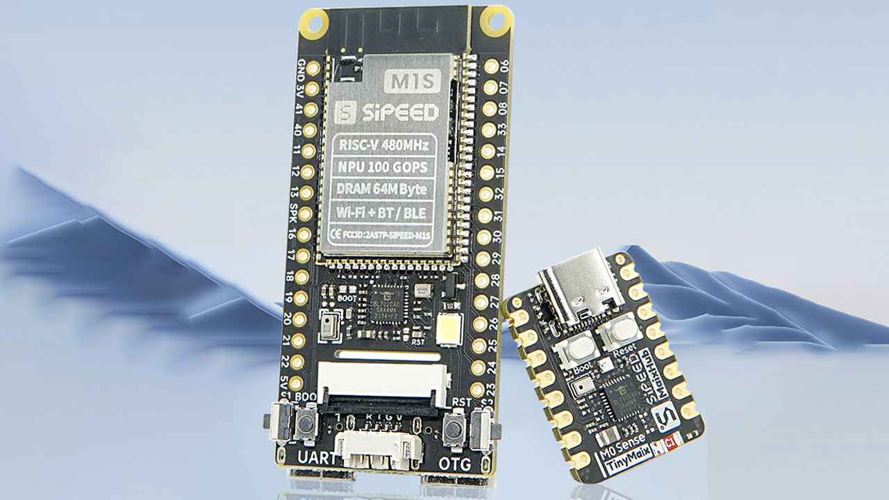
Sipeed a well-known manufacturer of sensor and development boards has recently released two cutting-edge RISC-V development boards – the MAIX M1s and M0sense. This board not only supports AI on Edge, but it can also run TinyML applications. With a price tag of only $6 and $4, these boards outperform their Arduino and ESP counterparts in functionality.
The Sipeed M1s is built around the Buffalo Lab BL808, which features a tri-core RISC-V system-on-chip, boasting a 480MHz 64-bit RISC-V core, a 320MHz and 160Mhz 32-bit processors cores with a 100GOPS NPU. This board also features WIFI/BLE/Zigbee, USB OTG HS, MIPI Camera, and an RGB LCD, with basic Linux support.
M0sense, on the other hand, is a typical TinyML board equipped with Audio/IMU sensors, designed to support Keywords Spotting, Human Activity Recognition, and Gesture Recognition applications.
Sipeed MAIX provides a user-friendly experience with support for drag-and-drop applications, lightweight Python scripting, and easy sharing of models via the app stores. Additionally, the platform offers an efficient inference library called TinyMaix, specifically made for MCUs with TinyML support. TinyMaix has been designed for easy porting and has already been successfully integrated into more than 40 chip/platform combinations, with minimal core code and memory usage.
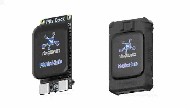
To make training AI models easy, Sipeed has developed MaixHub – an online AI model training and sharing platform. The platform facilitates semi-automatic labeling, making it more accessible to a broader audience.
With a commitment to making TinyML accessible for every MCU, Sipeed has also developed the TinyMaix inference library and the RISC-V TinyML board, M0sense. The M0sense board comes equipped with most TinyML peripherals and is capable of running typical TinyML models. Priced at only $4, it is an ideal starting point for TinyML enthusiasts.
Sipeed has also built a No-SDK solution, that allows users to drag and drop Python scripts or C modules making the platform very easy to use. Other than that the device also has An optional carrier board, the M1s Dock that provides breadboard-friendly pin headers for GPIO connectivity.
Features of Sipeed MAIX M1s & M0sense
Processor System:
M1s: Triple-core Bouffalo Lab BL808; 480MHz 64-bit, 320MHz 32-bit, 160MHz 32-bit RISC-V cores; Neural processing unit (NPU) at 100 GOPS
M0sense: 32-bit Bouffalo BL702 running at 144MHz
Memory:
M1s: 758kB SRAM, 64MB PSRAM, 16MB flash storage
M0sense: 132kB static RAM, 512kB flash
Camera Support (M1s only):
MIPI and DVP support up to 1080p
Two-megapixel OV2685 camera module with LED flash (M1s Dock)
Connectivity:
Wi-Fi (M1s only)
Bluetooth Low Energy (BLE)
Zigbee (M1s only)
USB 2.0 On-The-Go (OTG) (M1s only)
I/O Interfaces (M1s only):
SPI and RGB for external displays
I2S and analog audio
UART, I2C, SPI, SDOI, Ethernet
ADC and DAC
Video/Audio Acceleration (M1s only):
Motion JPEG (MJPEG), G2D, H.264, and OSD workloads
Displays and Sensors:
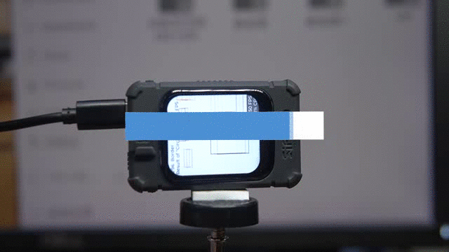
M1s: 1.69″ 280×240 display with capacitive touch support (M1s Dock)
M1s: Analog MEMS microphone (M1s Dock)
M0sense: Optional 0.96″ display
M0sense: On-board microphone and inertial measurement unit (IMU)
The Sipeed M1s Dock, which includes a breakout board, a display, and a case, is available on AliExpress for $19.99. Additionally, the M0sense board is available on AliExpress for $7.33. Both items are part of Sipeed’s selection of boards, and they can be conveniently purchased online.
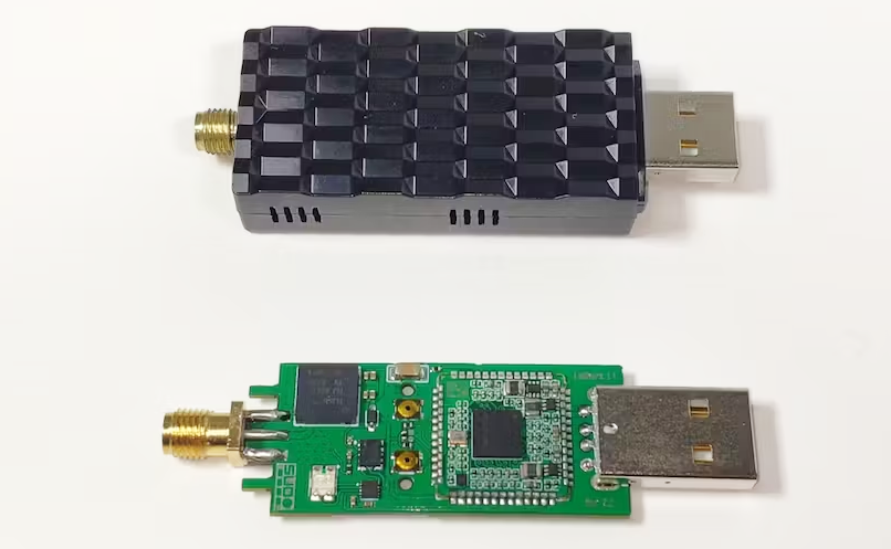
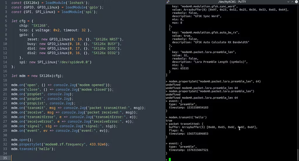
The Loshark is a USB Thumb Drive seized LoRa Debugging tool capable of running mainline Linux and executing javascript (ES2015) through Resonanceruntimeenvironment. Based on the Ingenic X1501 System-on-Chip module, it can run independently or alongside a computer, which makes it useful for various IoT and data-driven applications.
What is Resonance Framework?
Resonance, LoShark’s upcoming runtime environment, is currently in active development. Once completed, it will let devices run JavaScript (ES2015) on LoShark and similar instruments. It will have an open-source license, making IoT debugging and data collection easier.
The X1501 Pico SOM Module
Powered by the X1501 Pico SOM Module, the shark can execute complex algorithms and audio codes like Codec2 and Opus and software-based error correction codes such as DSSS and LDPC.
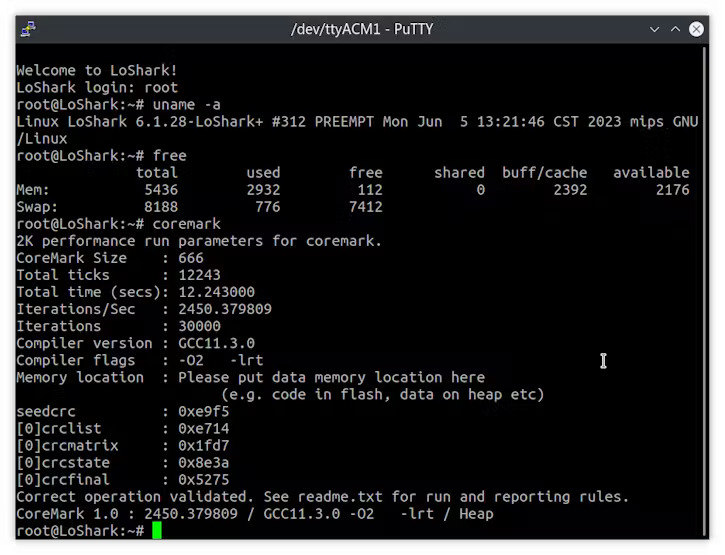
The SOM packs a fast, power-efficient, 32-bit MIPS32r2 RISC processor with a full-featured hardware FPU, 2200+ CoreMark, and 333+ MWIPS. More details bout this processor can be found in the product datasheet.
JavaScript Support with Resonance
The Loshark device’s primary strength is executing JavaScript (ES2015) through a resonance runtime environment. The runtime environment is still in the early development stage, but once the development is completed, it will be made open-source and accessible for everybody to use. If you are interested in testing or tinkering with Thai pieces of software, you can join their Discord for alpha testing.
The company has released a simple Javascript application and a NodeJS-like console interfacing directly with the SX126XLoRA chip.
This feature enables users to program specific tasks, like capturingpacketssending and monitoringLoRapackets manually or automatically with a delay. This is an open-source project so all the schematic PCB files and software can be found in Loshark GitHub Riopo. there is also a Hackaday page that talks about its features in deeper detail.
Linux Support
The device runs mainline Linux, allowing users to run C and C++ applications directly within the LoSharK device. By optimizing your C code, you can do a lot of exciting projects with this device.
Other features include a Real-Time Clock (RTC) capable of retaining time configurations for a minimum of two days and a programmable RGB LED indicator accessible via I2C for status indication. The device can be configured with any LoRa module with the following frequency bands: 433MHz, 869MHz, or 915MHz.
Features List of the LoShark Module
The complete feature list of the Loshark module is shown below:
A Compact and Portable USB-type Design makes the device easy for portability and convenience.
It has the ability to execute JavaScript (ES2015) through the Resonance runtime.
It runs mainline Linux, allowing users to write applications in C and C++.
This device has 8MB of DRAM, 8MB of PSRAM, and additional storage options (starting from 128MB up to 4GB).
LoShark consumes 150mW while plugged into a PC and not transmitting, which is ultra-efficient.
The device is built on top of X1501 Pico SoM powered by a MIPS32r2 RISC processor for max efficiency.
The LoShark is compatible with various different antenna types, thanks to its onboard SMA connector.
It offers powerful RTC that can operate independently for at least 2 days.
The device has an RGB LED for indication accessible via the I2C interface.
The LoSharK Debugger is provided in two variants. The version with 256MB storage is available for $59.99, while the 4GB Flash storage variant is priced at $72.99.
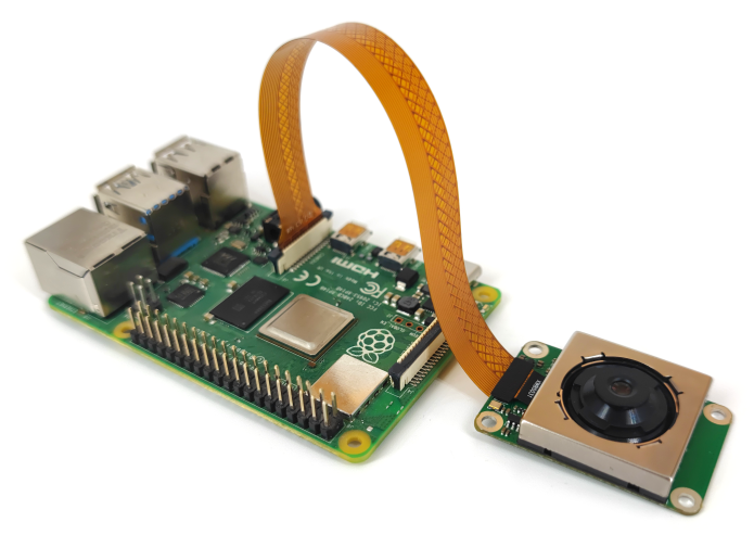
British and Finnish robotics, RBTS.co has introduced a crowdfunding campaign for its cutting-edge C50M Camera module, aiming to provide 8k-resolution video footage and 50-megapixel still images to single-board computers (SBCs) like NVIDIA Jetson, Raspberry Pi, and Rockchip RK3588-based SBCs. This state-of-the-art camera module, equipped with the Samsung ISOCELL GN2 image sensor (also found in the Google Pixel 8 Pro), opens up new possibilities in various industries, including drones, machine vision, and industrial automation.
The C50M Camera module’s capabilities are revolutionary, particularly in the realms of aerial and machine vision. For drone enthusiasts, this advancement means capturing everyday moments from the skies with unprecedented detail and clarity. Similarly, machine vision applications benefit from the high resolution, enabling more comprehensive data collection and precise image analysis, enhancing object recognition and defect detection.
The ISOCELL GN2 sensor within the C50M Camera module stands out with its exceptional 50MP photo-taking ability, making it an ideal choice for drones to capture the world below with incredible precision. Moreover, machine vision systems benefit from this high resolution as it leads to more accurate feature detection and identification.
Low-light conditions are no longer a hindrance with the C50M Camera module. The large 1.4μm pixels of the ISOCELL GN2 sensor allow for impressive low-light performance, ensuring clear and bright images, whether the drones are flying in poorly lit environments or machine vision systems are operating in dimly lit factories.
The lightning-fast autofocus of the ISOCELL GN2 sensor, utilizing the Dual Pixel Pro technology, is a boon for both drones and machine vision applications. It enables quick focusing on any object, making it perfect for drones tracking fast-moving subjects and critical for machine vision systems requiring swift response times.
High Dynamic Range (HDR) capabilities integrated into the C50M Camera module ensure vibrant photos are captured even in mixed lighting conditions. This is especially advantageous for drones and machine vision systems functioning in environments with contrasting light settings, maintaining image clarity and quality.
The RBTS.co team has invested significant effort in bringing this advanced camera technology to the market for drones, mobile robots, and various other projects. The crowdfunding campaign aims to secure the necessary funding to initiate the production of these camera modules. The current budget supports the smallest viable production run, and backers’ support will help gain the traction required to deliver these outstanding camera modules to their hands.
At present, RBTS.co has developed 8 prototype cameras, with the modules already undergoing testing by the production partner. The green carrier PCBs are also in the testing phase, while the prototypes are utilized for driver development and debugging, which is an ongoing process. The team anticipates that most features will be fully operational by the time they start shipping the first batch of production modules. Regular updates on driver developments can be found through the campaign page or product page at rbts.co/c50m.
The production camera modules are expected to be nearly identical to the prototypes showcased. However, there will be one main change – the addition of the ‘frame sync’ function. While the prototypes can only output this signal, the production modules will have the capability to use it as an input as well. This enhancement will enable hardware frame synchronization between multiple modules, further expanding the camera’s potential for various applications.
In conclusion, RBTS.co’s C50M Camera module, powered by the Samsung ISOCELL GN2 sensor, represents a significant leap forward in drone technology, machine vision, and industrial automation. With its high-resolution capabilities, low-light performance, lightning-fast autofocus, and HDR features, this camera module opens up endless possibilities for capturing the world from new perspectives and observing minute details in unparalleled clarity. By supporting the crowdfunding campaign, backers play a crucial role in making this groundbreaking camera technology accessible to enthusiasts and professionals alike, paving the way for advancements in diverse fields of robotics and vision-based applications.
The camera module is currently seeking funding on Indiegogo, available at a discounted rate of $97 for “Early Bird” backers, with the price increasing to $130 for those who join later.
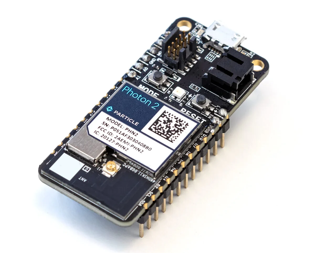
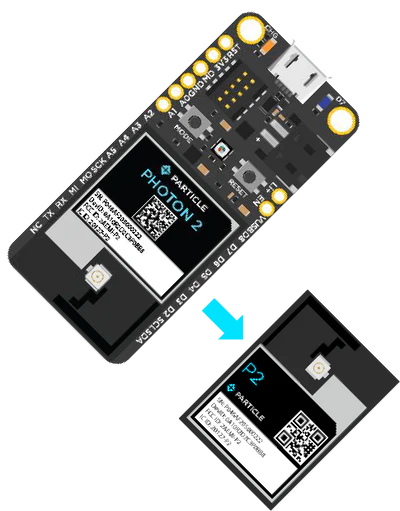
Particle, the integrated IoT Platform-as-a-Service, has unveiled its latest offerings: the P2 and Photon 2 hardware modules, which represent updates to their advanced embedded IoT Wi-Fi solutions. These modules, powered by the Particle Platform-as-a-Service, bring enhanced functionality and flexibility to enterprise IoT applications. The P2 module, available from July 29, offers advanced functionality suitable for low-cost, integrated designs in areas that may have limited cellular connectivity, such as factory floors, hospitals, smart buildings, and security monitoring. On the other hand, the Photon 2, expected to be available in late 2023, provides an improved feather form factor compatible development kit designed for rapid prototyping.
One notable achievement with these updates is the introduction of a combination of Wi-Fi and cellular connectivity options for enterprise IoT applications. Historically, securing connectivity with the necessary processing power for enterprise applications required costly and data-intensive cellular connectivity. With the advent of P2, Particle delivers enterprise-grade security and connectivity protocols, more powerful processing capabilities, and ensures secure and guaranteed availability.
Particle’s Wi-Fi modules and development kits are purpose-built for enterprise-grade applications, prioritizing RF performance, low power consumption, security, and rapid time-to-market. These latest components mark the introduction of a new enterprise Wi-Fi product line, succeeding the P0/P1 and Photon/Argon, and come with supply security and added support for low-power Bluetooth, a more powerful processor, increased memory, and broader support for enterprise Wi-Fi configurations, including 5GHz and 802.1X networks.
Adam Warmington, Senior Product Manager at Particle, emphasized the importance of device and network versatility and security, considering the staggering 700% increase in IoT cyber attacks since 2019. The P2 and Photon 2 updates are designed to address the constantly evolving IoT cyber threat landscape and provide developers with the power to achieve seamless forward compatibility and faster market entry.
To ensure a predictable and reliable supply chain for chip-based components, Particle has introduced the Supply Secure hardware portfolio. This proactive program updates and replaces legacy hardware, ensuring a consistent supply chain for its products.
The Particle Photon 2 features a dual-band Wi-Fi and Bluetooth 5.3 Low Energy (BLE) development board powered by a Realtek RTL8271DM microcontroller with a single Arm Cortex-M33 CPU core running at up to 200MHz, along with 3MB of RAM and 2MB of available program storage. The module includes a 2MB flash file system and an integrated PCB antenna with support for an external antenna if needed.
The P2, on the other hand, is the same hardware as the Photon 2 but is offered in a module format rather than a breadboard-friendly development board. This allows developers to prototype their ideas using the Photon 2 and then transition to productization using the P2 module, available at a slightly discounted price in multiples of 10 units.
Additionally, Particle offers an edge machine learning (ML) bundle that combines the Photon 2 with various sensors like an accelerometer, microphone, gas sensor, and motion sensor, along with a breadboard and other prototyping hardware for on-device artificial intelligence projects, with full support in the Edge Impulse Studio platform.
The new hardware is now available for purchase on the Particle store, with the Photon 2 priced at $17.95 and the Edge ML bundle costing $69.
The P2 module can be purchased at $15.36 per unit, available exclusively in multiples of 10 units. As an added bonus, the introduction of the P2 module has led to a significant discount on the earlier P1 module, priced at $6.50 per unit while stocks last. These advancements offer promising opportunities for developers and enterprises seeking advanced IoT solutions with enhanced connectivity and security features.
In this series of articles, we considered PCM (Pulse Code Modulation) as a method of digital representation of an analog signal. In the PCM method, the samples of the continuous wave are allowed to take only certain discrete values. These amplitudes are then assigned a code, where each code uniquely represents the magnitude of the sample. These code words as digitaldata find application in various contexts.
Analog-to-digital converters (ADCs) are devices or circuits that practically transform analog signals into digital ones using the PCM concept. They have many applications in the industry. For example, many modern microcontrollers are equipped with built-in ADC converters. This allowed designers to interface easily with analog sensors, convert analog signals from the environment into digital data, and process it within the microcontroller for various applications.
The process of analog-to-digital conversion can be executed through various architectures, such as successive approximation register (SAR), parallel (flash) conversion, sigma-delta conversion, and more.
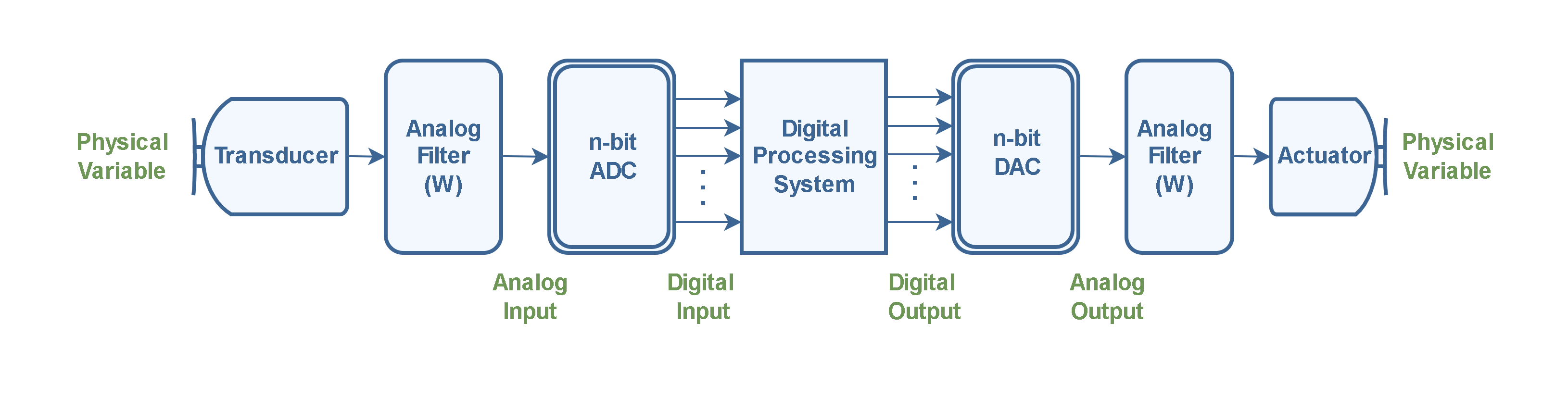
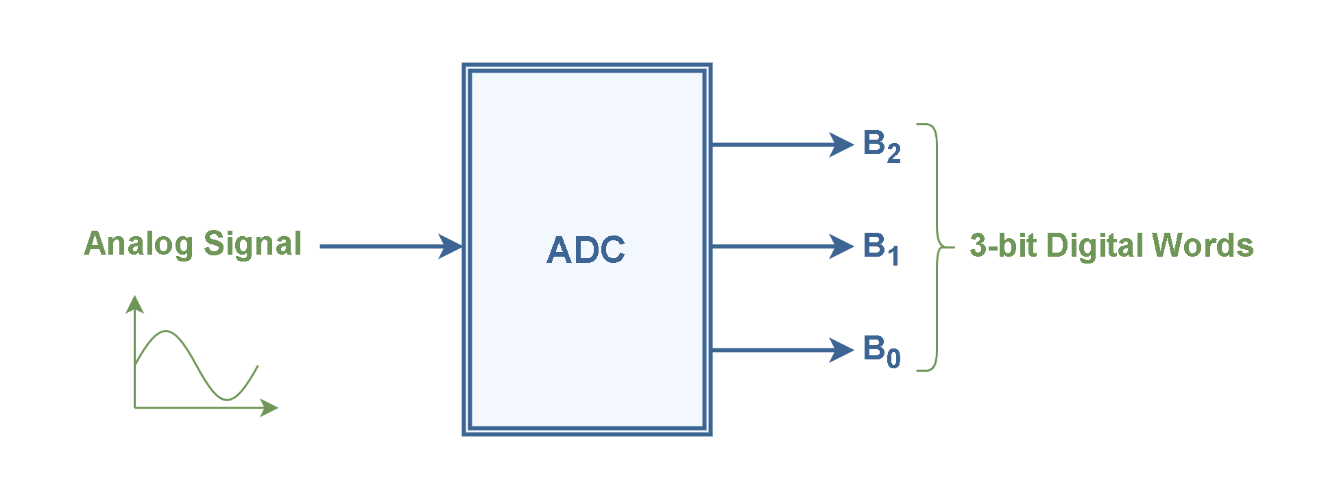
The task of the digital-to-analog converter (DAC) is the inverse of the ADC: it converts numerical digital values back into continuous analog signals. DACs are employed to translate the outcomes of digital processing into real-world variables for control, information display, or other forms of analog processing. Figure1 illustrates a general block diagram of a digital processing system.
Figure 1: Interfacing digital processing system with the analog world using n-bit ADC and DAC
Analog quantities are often representative of real-world phenomena. In this configuration, the primary variable typically relates to a physical parameter like temperature, light, etc., which is transduced into electric voltages or currents by a transducer.
Here, analog filters are used to comply with the sampling theorem. The first filter placed before the ADC is an LPF called an anti-alias filter. This filter, placed prior to the ADC, eliminates frequency components above half of the sampling rate (fs/2) that could lead to aliasing during sampling. The filtered analog signal is then transformed into digital codes by the ADC block and directed into the digital processing system, which could be a microcontroller or other forms of data processing and manipulation.
After that, the processed digital signal is fed to the DAC stage to convert it back into an analog signal. The second filter placed after the DAC block is also an LPF and is called a reconstruction filter. It also removes frequencies above the Nyquist rate (fs/2). Finally, the analog output signal is transduced back to the physical world by an actuator stage for any further physical operations.
As an example, in an audio signal processing configuration, an ADC converts the analog audio signal captured by a microphone, into a digital signal for computer-based sound effects processing. The DAC then converts the processed digital signal back into analog form, which can be played through a loudspeaker.
In contemporary electronics, instrumentation, information technology, data acquisition and transmission, control systems, medical imaging, professional and consumer audio/video, and computer graphics, converting analog signals to digital has become a fundamental process.
In this article, we explore the key performance criteria that define the effectiveness of ADCs in their applications.
Quantization Errors
There are various sources of errors in conversion circuits. Among them, quantization error (Qe) or quantization uncertainty stands out as one of the most critical factors that significantly impact the performance of A/D or D/A converters.
Quantization errors occur in analog-to-digital conversion when the continuous analog signal is approximated by discrete digital values. In a PCM encoder, every voltage sample is already rounded off (quantized) to the nearest available level and then translated into its corresponding binary code. When the code is converted back to analog at the decoder, any round-off errors are reproduced.
Theoretically, the conversion will never be 100% accurate; that is, a finite amount of information will be lost forever during the conversion process. It means when the digital representation is converted back to analog, the result will not be identical to the original waveform.
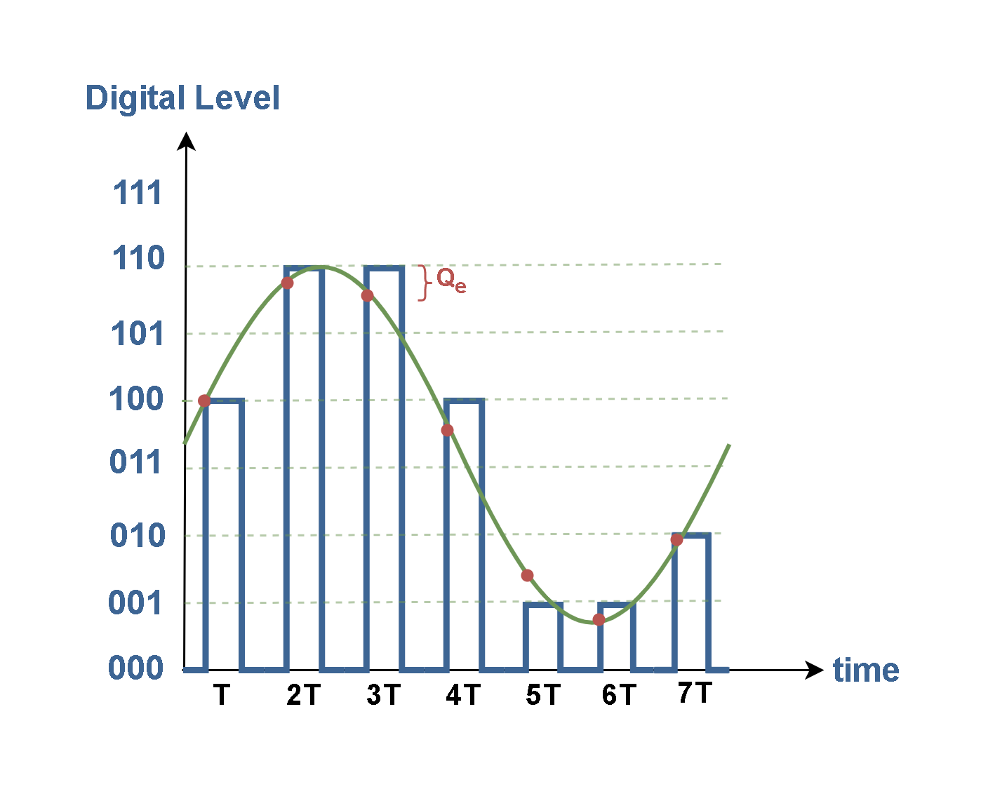
Let’s refer to Figure 2 as the block diagram of a 3-bit A/D converter.
Figure 2: Block diagram of a 3-bit ADC
Obviously, a 3-bit ADC has 8 digital (quantum) levels. The output digital results of this system in comparison to the analog input, are represented in Figure 3 and a typical sample of Qe is indicated on the graph.
Figure 3: Digital representation of the analog waveform by a 3-bit ADC
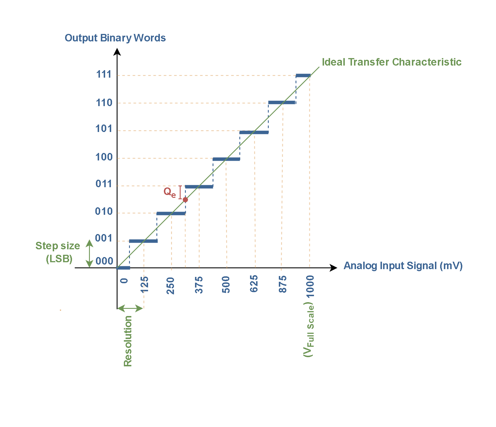
Now, we may look at the effects of quantization. Figure 4 shows the transfer characteristics for a 3-bit unipolar ADC with a full-scale voltage of 1 volt.
Figure 4: The characteristic diagram of the 3-bit ADC with a full-scale voltage of 1 volt
Figure 4 represents a 3-bit quantizer, which maps a range of analog input values to only eight (23) possible output digital values. If the maximum peak-to-peak value of the input signal is 1 V, each step in the staircase has (ideally) the same size along the y-axis, which is defined as 1 LSB (the least significant bit) in terms of voltage. In this case, 1 LSB is equal to 1/8 V (or 125 mV).
Under these conditions, as an example, it would be impossible to perfectly encode a value of 300 mV. The nearest value available would be binary 010, which yields 250 mV. Obviously, the resulting round-off creates some error in the digital representation.
In an ideal assumption, the characteristic of the conversion system could be a straight diagonal line with no steps at all. But in reality, an ADC quantizes a sampled signal by selecting a single discrete value from a pre-established finite list of such values to represent each analog input sample. This rule gives the transfer function of analog input to digital output a uniform ‘staircase’ characteristic.
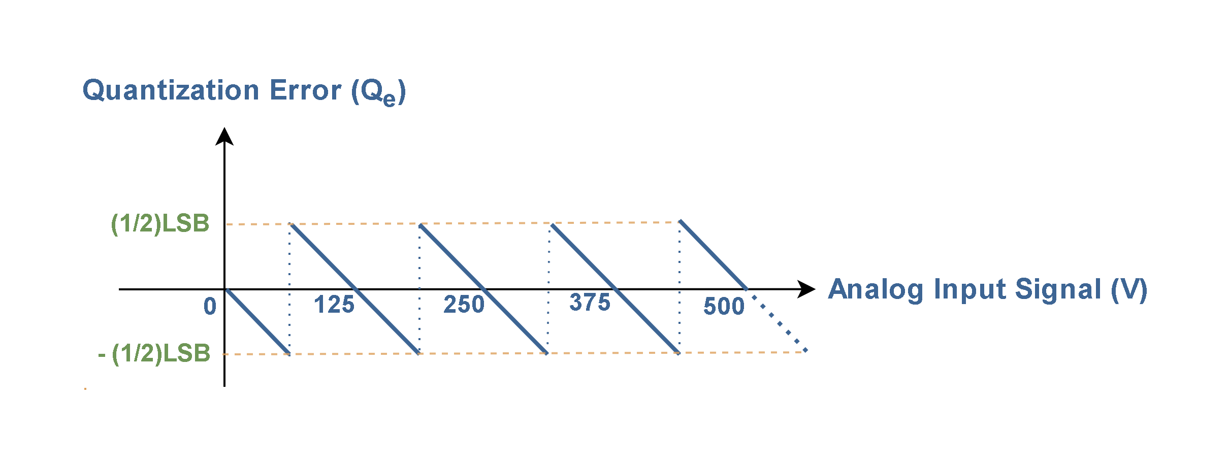
The vertical difference between the actual analog value and the quantized digital value at each sample point defines the quantization error (Qe). The graph of quantization errors in Figure 5 is resulted from the subtraction of ideal values of the linear function from the actual values of the staircase function. The maximum magnitude of the quantization error equals half of a quantum level (q/2) where q is the width of an individual step. Then, Qe can fluctuate within the range of ± (1/2) LSB or ± (q/2) as illustrated in Figure 5.
Figure 5: The characteristic diagram of the quantization error
The result is a sawtooth-pattern error voltage that manifests itself as white noise added to the analog input signal. The quantization error is an actual voltage, as it alters the signal amplitude. Consequently, the quantization error is also referred to as the quantization noise(Qn).
The quantization error is generally larger when the number of bits used for conversion (n) is small, as there are fewer quantization levels to represent the continuous signal accurately. As the number of bits increases, the quantization error becomes smaller, resulting in a more accurate representation of the original analog signal. In practical terms, it is possible to reduce the error to such small values that it may be ignored in many applications.
The Signal-to-Quantization Noise Ratio (SQNR) is a measure of the ratio between the power of the original analog signal (Ps) and the power of the quantization noise (Pqn) introduced during the analog-to-digital conversion. However, it is assumed that the ADC is relatively free of random noise and that the transitions can be easily measured.
Then, the Signal-to-Quantization Noise Ratio (SQNR) can be generally calculated in terms of dB using Equation 1.
Equation 1: Calculating Signal-to-Quantization Noise Ratio
In an ideal n-bit converter scenario where the input signal is a full-amplitude sine wave, the corresponding SQNR can be determined using Equation 2.
Equation 2: Calculating SQNR for an n-bit ADC
This gives the ideal value for an n-bit converter and shows that each extra 1 bit of resolution provides approximately 6 dB improvement in the SQNR.
SQNR is a valuable metric for assessing the quality of the analog-to-digital conversion in contrast to the quantization error. A higher SQNR value indicates better accuracy and a smaller impact of quantization noise on digital representation.
A/D And D/A Conversion Performance Criteria
The specifications which impact the performance of an ADC are similar to those for a DAC. In addition to SQNR, some other major factors that determine the performance of D/A and A/D converters are resolution, sampling rate, speed, accuracy and dynamic range. They are explained below.
Resolution: In an A/D system, the resolution is the smallest change in voltage at the input that the system can detect and convert into a corresponding change in the digital code at the output. Similarly, for a D/A circuit, resolution refers to the smallest change in the output analog signal that the circuit can produce.
D/A or A/D IC manufacturers usually specify the resolution in terms of the number of bits in the digital code (n) or voltage corresponding to the least significant bit (LSB) of the system.
Another approach to expressing resolution is by indicating the voltage step magnitude between quantization levels, also termed the quantization width (q). For an n-bit DAC, the LSB carries a weight of 2-n. For instance, an 8-bit DAC can resolve 1 part in 28 or 0.39% of the full-scale output voltage when the binary input code is incremented by one LSB. Then, for full-scale voltage (VFS = Vmax – Vmin) equals 10 volts, the resolution of the 8-bit system is 0.039 (= 10/28) volts.
Generally, it can be calculated in terms of voltage by Equation 3.
Equation 3: Calculating resolution for an n-bit ADC
Sampling Rate: The sampling rate denotes the frequency at which the analog signal can be sampled and translated into a digital code per unit of time. For proper A/D conversion, the minimum sampling rate must be at least two times the highest frequency of the analog signal being sampled to satisfy the Nyquist sampling criterion. The more samples taken in a given unit of time, the more accurately the analog signal is represented in digital form.
Speed: For A/D converters, the speed is specified as the conversion time, which represents the time taken to complete a single conversion process, including sampling the analog signal, processing, and generating the digital output. In A/D converters, conversion speed, along with other timing factors, must be considered to determine the maximum sampling rate of the converter.
For D/A converters, the speed is specified as the settling time, which is the delay between the binary data appearing at the input and the output voltage reaching a stable value. This sets the maximum data rate that the converter can handle.
Accuracy: Accuracy is the degree of conformity between the converter’s output and the actual analog signal value. The resulting round-off error occurs due to the quantization process, leading to some deviation from the actual analog value.
As the number of bits increases, the step size between quantization levels decreases, leading to higher accuracy when converting between analog and digital signals. For example, an eight-bit word (n = 8) provides 256 distinct values (28) for representation, offering a more precise conversion of the analog signal than using a four-bit word with 16 distinct values (= 24).
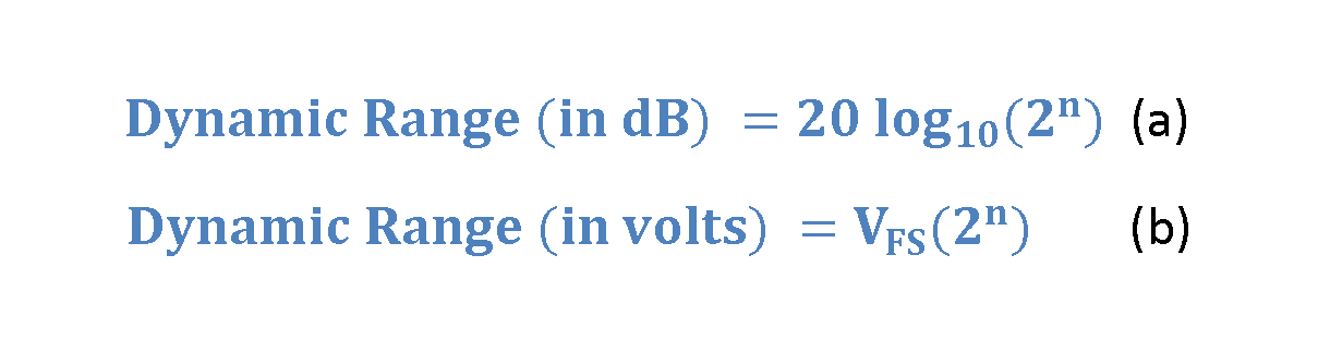
Dynamic Range: Dynamic Range refers to the range of signal amplitudes that an ADC can accurately represent in its digital output without significant loss of accuracy. In other words, the dynamic range is the difference between the maximum and minimum input signal levels that the ADC can handle effectively.
Dynamic range is expressed as the ratio of the maximum input voltage to the minimum detectable voltage and, it is subsequently transformed into decibels. Calculation of the Dynamic Range (DR) is defined in Equation 4, combining logarithmic (dB) and linear (voltage) aspects.
Equation 4: Calculating dynamic range for an n-bit ADC
The full-scale voltage (VFS = Vmax – Vmin) is the voltage range that the ADC uses to represent the analog input signal.
For example, if the ADC uses a reference voltage of Vref = 5 volts, the input voltage should fall within this range for accurate conversion. For a 12-bit ADC (n = 12) and the reference voltage of 5 volts, the dynamic range can be assessed as follows:
Dynamic Range (in dB) = 20 log (212) = 20 log (4096) ≈ 72 dB
or,
Dynamic Range (in volts) = 5 .212 = 5 (4096) = 20480 volts
It is essential to remember that all performance parameters of electronic components, including converters, can be influenced by variations in supply voltage and temperature. Datasheets commonly specify these parameters under specific temperatures and supply voltage conditions to offer standardized information. However, in practical systems, operating conditions may deviate significantly from the specified figures. As a result, actual performance can differ from what is outlined in the datasheet.
Summary
The real-world analog input to an ADC is a continuous signal with an infinite number of possible states, whereas the digital output is, by its nature, a discrete function with a finite number of different states.
An ADC is a device that performs PCM. It samples and translates an analog signal into a digital format, where each sample is represented by a binary code.
A digital binary code is converted to an analog output (current or voltage) by a DAC.
Quantization Error (Qe), also known as quantization noise, is the error introduced during the process of converting a continuous analog signal into a discrete digital representation. It is essentially the error caused by approximating the continuous signal with discrete digital values. Obviously, the resulting round-off creates some errors in the digital representation. It results in a deviation between the actual analog value and its digital representation.
There may be a difference of up to ½ LSB between the actual input and its digital form.
This error can be reduced by increasing resolution so that finer steps may be detected.
For A/D circuits, the resolution is the smallest input voltage that is detected by the system. Resolution is the smallest standard incremental change in the output voltage of a DAC. The number of discrete steps or bits that an ADC/DAC can represent, determines its precision in converting analog signals to digital data or vice versa. Typically, the resolution is specified using a number of bits in digital codes (n), although a voltage specification (LSB) is also possible.
The sampling rate is the frequency at which the ADC samples the analog input signal to convert it into discrete digital data points.
For A/D converters, the speed is specified as the conversion time i.e., the time to perform a single conversion process. For D/A converters, the speed is specified as the settling time e., the delay between the binary data appearing at the input and a stable voltage being obtained at the output.
As the number of bits increases, the step size between quantization levels decreases. Therefore, the accuracy of the system is increased when a conversion is made between an analog and digital signal.
The dynamic range (DR) of an ADC is the ratio of the largest to the smallest signals the converter can represent. It measures the range of signal amplitudes that an ADC can accurately represent in its digital output without significant distortion.
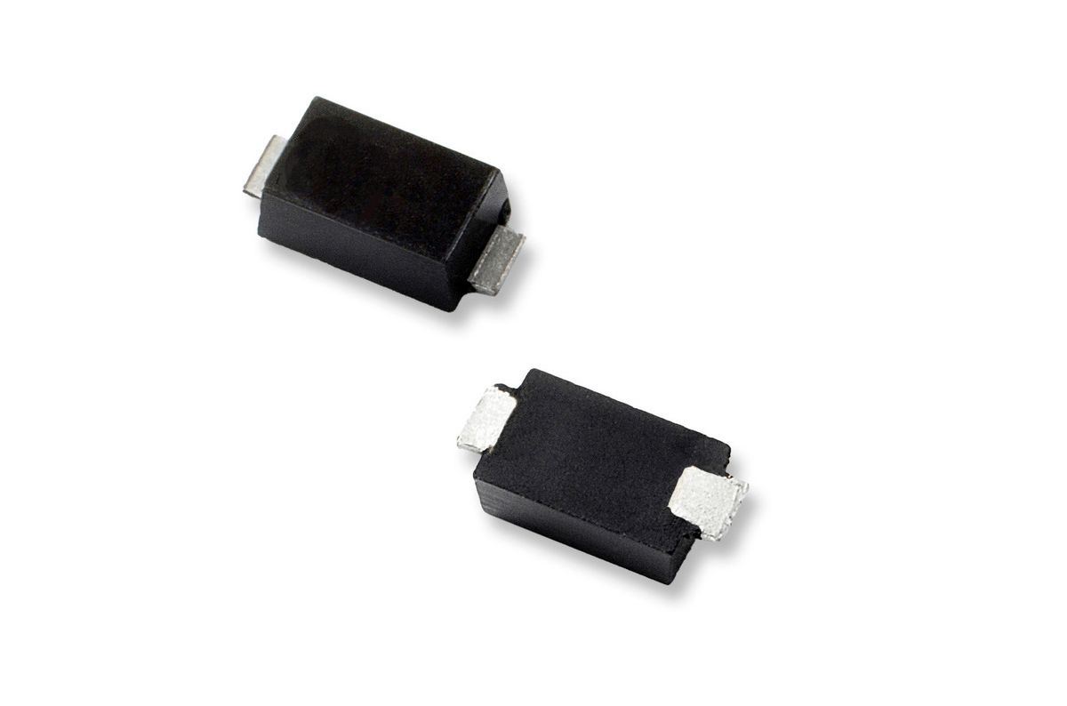
Littelfuse, Inc, an industrial technology manufacturing company empowering a sustainable, connected, and safer world, announced the release of its new SZSMF4L 400 W TVS Diode Series. As automotive electronics continue increasing in volume and sophistication, all these components require protection from high voltage, high energy transients.
The SZSMF4L TVS Diodes protect these sensitive systems with fast response time, low Zener impedance, high surge handling, and excellent clamping capabilities. Its low leakage current is also ideal for protecting sensors. Due to its small size, it is suitable for most automotive applications, especially vehicle electrification. View the video.
The SZSMF4L Series is ideally suited for a range of automotive electronics applications, including:
EV powertrain,
On Board Charging (OBC),
Battery Management System (BMS),
EV Invertor,
Power Distribution Unit (PDU),
Domain Controller,
Zone Controller,
Body Control Module
Low leakage current required for sensor protection.
“With the megatrend of vehicle electrification and autonomous driving, TVS diode miniaturization is becoming more critical to automotive electronics engineers and PCB designers,” said Charlie Cai, Director Product Marketing SBU, Littelfuse. “The automotive grade SZSMF4L TVS diodes offer greater flexibility and space-savings, providing the ideal 400-watt solution in a small (SOD-123FL) TVS diode package with both uni- and bi-directional protection.”
The SZSMF4L Series SMD TVS Diodes offer the following key features and benefits:
Compact SOD-123FL package compatible with automated PCB assembly processes.
Uses ~40% less printed circuit board space than previously available components.
Working peak reverse voltage range: Uni-directional (5 to 78 V) and bi-directional (10 to 78 V).
Low Leakage Current performance.
High operating temperature: up to 175°C.
Availability
The SZSMF4L Series SMD TVS Diodes are available in tape and reel packages of 1500 and 5000. Place sample requests through authorized Littelfuse distributors worldwide. For a listing of Littelfuse distributors, please visit Littelfuse.com.
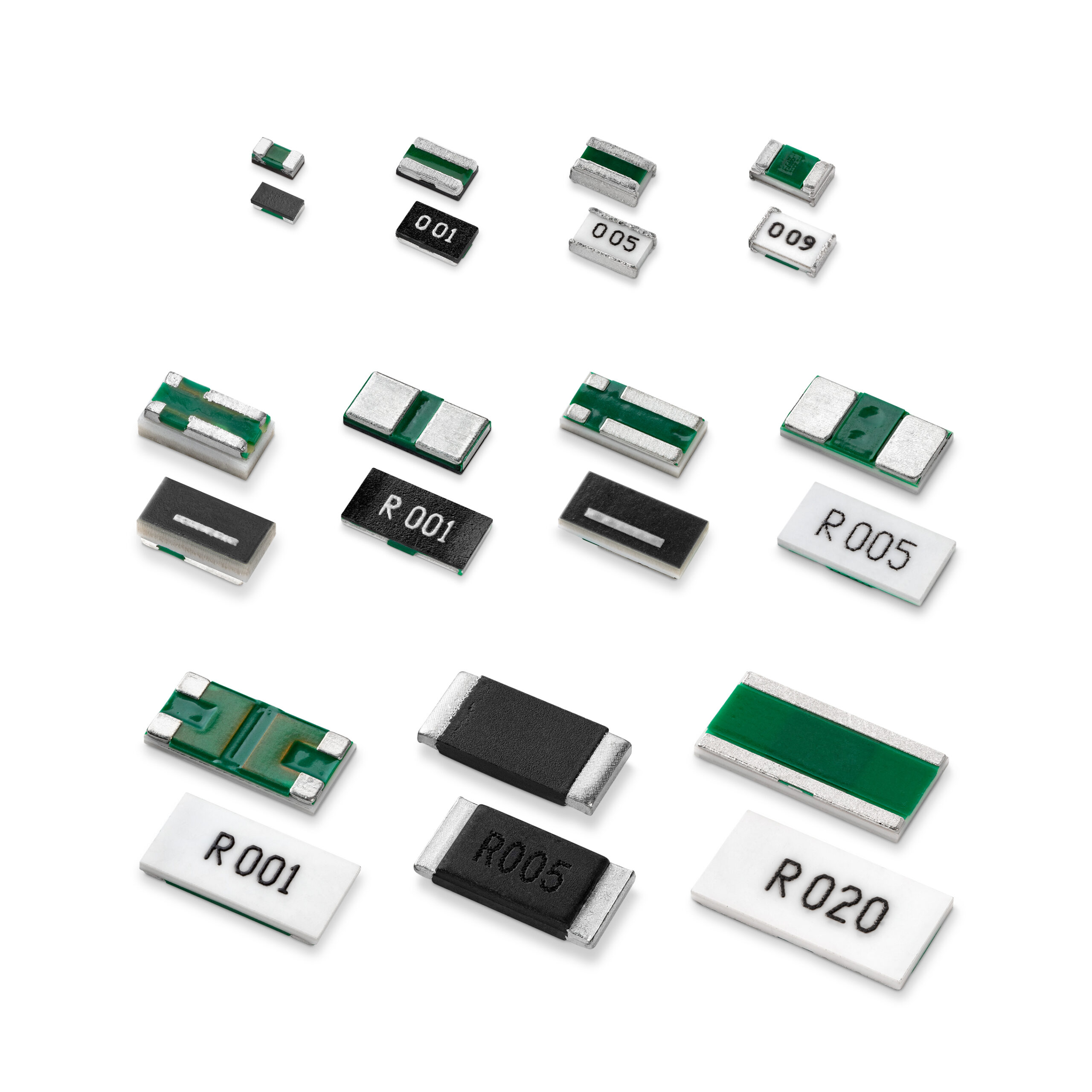
Littelfuse, Inc. , an industrial technology manufacturing company empowering a sustainable, connected, and safer world, announced the launch of its new Current Sensing Resistor (CSR) family. These new CSRs offer a more cost-effective solution for measuring current within circuits, enabling voltage monitoring, control, and power management of functions such as battery charging and motor speed, while also providing overcurrent protection. View the video.
The Current Sensing Resistors Series is a game changer for both automotive and consumer electronics markets and are ideal for numerous applications, including:
Automotive electronics
Electric vehicles, including 2- and 3-wheelers
Home appliances
Consumer electronics
Industrial automation.
“Our customers include industry leaders in automotive and consumer electronics, who require precise current and voltage monitoring for their advanced technologies,” said Stephen Li, Product Manager at Littelfuse. “To address these needs, the CSR family provides a more cost-effective solution than competing technologies like Hall Effect sensors, current transformers, flux gate sensors (DC only), and Rogowski coils (AC only). Additionally, CSRs work in AC and DC circuits without requiring additional power or equipment to enable measurement.”
The CSR Series offers the following key benefits:
Cost-effective, compact solution
Current measurement
Voltage monitoring
Power control
Overcurrent protection.
The new Littelfuse CSR family of products extends the company’s circuit protection solutions portfolio, deepening its current and voltage monitoring focus. Each of the eight CSRs is either a metal foil, metal strip, or metal plate resistor used for measuring currents in circuits due to its high precision and low resistance rating.
Availability
The Current Sensing Resistors (CSR) Series are available in tape-and-reel quantities of 5,000. Place sample requests through authorized Littelfuse distributors worldwide. For a listing of Littelfuse distributors, please visit Littelfuse.com.

 Robust and resilient thermal design