96-Layer Memory Chips By Toshiba

The need for larger memory storage for smartphones will never stop, especially with the continuous development of larger and stronger applications. This need is always pushing semiconductor manufacturers to keep trying to fit as much bits as possible in  smaller volumes and with lower costs.

To achieve this, memory chips are now growing in three dimensions instead of two. Recently, Toshiba has developed a new 96-layer BiCS 3D flash memory device with a storage capacity of 32 GB. The new device meets market demands and performance specifications for applications that include enterprise and consumer SSD, smartphones, tablets and memory cards.

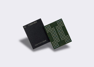
This memory chip was built with three bits per cell, known as triple-level cell (TLC) technology. Stacking layers and manufacturing process increase the capacity of each chip with 40% per unit size. They also reduce the cost per bit, and increase the manufacturability of memory capacity per silicon wafer.

In order to add more layers to the chip, Toshiba is working on increasing the number of bits in every cell. In the near future, it will apply its new 96-layer process technology to larger capacity products, such as 64 GB. It will also develop chips with QLC (quadruple-level cell) technology.

By stacking 64 layers of QLCs, the engineers at Toshiba have created a 96-gigabyte device. Integrating 16 of them in one package will achieve a capacity of 1.5 TB, that corresponds to 12 trillion bits.

If you are interested, you can check these out at the 2017 Flash Memory Summit in Santa Clara, California from August 7-10.

Source: elektor

RandA, Combining Raspberry Pi & Arduino

Two years ago, open electronics had produced “RandA“, an Atmega328-based board for Raspberry Pi to deliver the advantages of both, Raspberry Pi and Arduino. Earlier this month, an updated version of RandA has been released to be compatible with Raspberry Pi 3.

RandA is a development board that leverages the hardware equipment and the computing power of Arduino with its shields, and the enormous potential of the Raspberry Pi. It features Atmega328 microcontroller, has RTC (Real Time Clock) module, power button and sleep timer, connectors for 5 volts and connectors for mounting Arduino shield.

Combining these two platforms is a way to exploit specific characteristics of both. Raspberry Pi could use Arduino as configurable device, and Arduino might work as a controller for Raspberry Pi allowing access to complex environments like the network, allowing complex processing or access to multimedia.

RandA was created at first for Raspberry Pi 2 and B+, using the first 20 pins to connect them, the serial port for programming the Atmega328 and for communication with Raspberry Pi. With the enhancements that come with the third version of Raspberry Pi, such as upgrading CPU to a quad-core 64 bit ARMv8 clocked at 1.2 GHz and adding WiFi and Bluetooth transceivers, there were some structure modifications that require updating the RandA.

Raspberry Pi 3 uses the standard UART0 serial port for connection via the Bluetooth interface equipping version 3. Therefore, it is no longer available on GPIO14/15 as it was in the first and second version of Raspberry Pi. The secondary UART1 serial is configured on those pins instead, but this serial port is based on a simulated serial not on a preset UART hardware. In particular, its clock is connected to the frequency of the clock of the system which varies in function of the load in order to save energy.

To solve this, the software is configured to recover the UART0 on GPIO 14/15 pins without modifying any hardware parts. This way will disable the Bluetooth peripheral, but the WiFi is still working and you can use Bluetooth by connecting a Bluetooth dongle via USB.

To know more about the new version of RandA you can review this post, and reading this post to learn more about RandA in general. You can get your RandA board for about $36 and this tutorial will help you get starting with it.

Open-Hardware Reaches The Outer Space with UPSat Satellite

Libre Space Foundation completed the mission of building a completely Open-Source 2U CubeSat Satellite from scratch. It’s called “UPSat”.

On April 18th at Cape Canaveral in Florida, Atlas V Rocket launched Private Cygnus Cargo Ship, and UPSat was among its cargo.

Subsystems of UPSat. Image courtesy of UPSat

With both software and hardware parts published on github. UPSat seems to be a real open hardware project.

Let’s have a quick overview of the UPSat’s subsystems:

  • Electrical Power Subsystem EPS: This subsystem controls the CubeSat’s electrical power. UPSat is powered by 7 PV solar cells and 3 Li-Po rechargeable batteries (3.7V, 4Ah).
  • Image Acquisition Component IAC: The goal of the IAC is to shoot relatively good quality images pointing down to the Earth. IAC consists of a linux embedded board( DART4460 running OpenWRT), and a USB camera Ximea MU9PM-MH with attached lens.
  • Attitude Determination and Control Subsystem ADCS: The ADCS is armed with 3-axis digital gyroscope, magnetometer, Sun Tracker’s pointing vector GPS and Magneto-Torquers. This subsystem is responsible for stabilization of the cube satellite and orienting it in the desired direction.
  • On Board Computer subsystem OBC:  The brain of the satellite for decision making and monitoring of all subsystems. It’s based on STM32F4 microcontroller and uses FreeRTOS firmware.
    OBC PCB


  • Communications Subsystem COMMS: It’s based on CC1120, the TI’s High-Performance RF Transceiver.  Because of the low current consumption, the success of employing it in previous missions and other couple of reasons, the folks behind this project selected CC1120 among the others.

The project is completely open-Hardware and even the UPSat’s structure design files are available.

Source: Open Electronics

MEMS — A 22-billion-dollar-worth industry by 2018

Thanks to Micro-Electro-Mechanical-Systems MEMS technology, which will be a 22-billion-dollar-worth industry by 2018, our mobile phones are equipped with accelerometers and gyroscopes so they know the direction and rotate our mobile screen as needed. The applications of MEMS had expanded a lot in various fields like: energy harvesting using piezoelectric effect, microphones, gyroscopes, pressure sensors, accelerometers and many more. Moreover, this micro-level technology is going to be nano-level with Nano-Electro-Mechanical-Systems NEMS.

The basic idea behind MEMS is about having moving parts inside the silicon chip. Accelerometers for example, one of the most famous applications of MEMS, sense the acceleration by measuring the change of the capacitance C1, C2 between a moving part/mass and fixed plates. So when acceleration is applied in a particular direction it can be detected and measured.

Image is adapted from engineerguy YouTube channel

The amazing “How a smartphone knows up from down” video presented by Bill Hammack (engineerguy) can demonstrate in a clear way the principle of MEMS.

Last but not least, MEMS has applications in medical and health related technologies like Lab-On-Chip. LOCs can integrate a laboratory function in a single chip. So MEMS may not only solve technical problems, but they may also play an important role in solving problems in human health field.

“Genotyper” device. via NIAID

A New Material For Unbreakable Smart Devices

Most of smartphones parts are made of silicons and other compounds, which are expensive and easily-breakable. This problem is making all of smart devices manufacturers looking for stronger and cheaper solutions.

By combining a set of materials, a group of researchers have successfully discovered a new material which could finally finish the disaster of cracked smartphone and tablet screens. The research group is led by a Queen’s University’s School of Mathematics and Physics researchers, with scientists from Stanford University, University of California, California State University and the National Institute for Materials Science in Japan.

Alongside conducting electricity at novel speeds, the new material is light, durable, and can be easily produced in large conventional semiconductor plants. It is a combination of  C60 fullerenes with layered materials such as graphene and h-BN (boron nitride), which presents a unique material with special properties that will be particularly relevant for use in smart device manufacturing.

This material composition has properties that are not naturally found in other materials. The hBN provides stability, electronic compatibility and isolation charge to graphene, while C60 can transform sunlight into electricity. The combining process is known as “der Waals solids” that allows compounds to be brought together and assembled in a pre-defined way.

The material also could mean that devices use less energy than before because of the device architecture so could have improved battery life and less electric shocks. This cutting-edge research is timely and a hot-topic involving key players in the field, which opens a clear international pathway to put Queen’s on the road-map of further outstanding investigations.
~ Dr Elton Santos, leader of the research group

The research shows that the material has the same properties as silicon, but higher chemical stability, lower weight and greater flexibility. These features would make the screens made of this material more difficult to break.

There is still one problem needs a solution. The graphene and the new material architecture is lacking a ‘band gap’, which is an important property to make active semiconductor devices. The team is planning to solve this using transition metal dichalcogenides (TMDs) which are chemically highly stable and have bandgaps like silicon.

According to the research group, this findings will pave the way for further exploration of new materials in the future. You can find more details about this by reviewing the research paper, which was published in the scientific journal ACS Nano, and by reading the official announcement.

Digitool – DIY 4 channel logic analyzer with LCD

Juan Antonio Rubia Mena tipped us with his DIY logic analyzer based on PIC18F2525 @ 32 Mhz. He writes:

One of the most useful tools for micro-controller design is the logic analyzer. You can find one for every budget or performance, but lately those based in USB connection to PC have gained popularity (not not mention the chinese copies). The main drawback of USB based logic analyzer is the need of using a computer, which uses to be a bit difficult when doing field testing. Digitool isn’t intended to replace a logic analyzer; it’s main purpose is being a quick test tool for microcontroller based development.

Digitool – DIY 4 channel logic analyzer with LCD – [Link]

Raspberry Pi ATX Power Board

Control 16 Relays with your Pi, supplying 12V to 16 DC jacks. All powered from and ATX Power Supply, with sensor support on board. You can find more details on the author’s website. by Rodney Balent @ kickstarter.com:

I started out with the simple goal of wanting to automate a few things around the home starting with my vertical garden using a Raspberry Pi.

With that goal in mind I decided to make a 16 bay relay board so I could control as many devices as possible from a single point. It was then I found how much space this would take up, and how long it would take to wire up and it became impractical.

So the next logical step was to look into making my own PCB. I noticed that virtually all the devices I wanted to control ran on 12V, I also noticed how many spare ATX power supplies I had lying around and the gears in my head started turning.

1.7K Voters Choose From about 100 SBC’s — The Results of Linuxgizmos 2017 Survey

Each year, Linuxgizmos does a survey about Single Board Computers (SBC) to find out how many of hackers and makers are using each of which . The results this year show apparently, the domination of Raspberry Pi 3 over the other 97 boards by a proportion of 4-to-1. Raspberry Pi 3 was launched in the first quarter of 2016 and brought some enhancements to RPi2 especially in the CPU side which was 300 MHz faster than the RPi2 one, and an updated ARM architecture: Cortex-A53.

The scores for each SBC was calculated using a Borda scores format: (3 x first choices) + (2 x 2nd choices) + (1 x 3rd choices).


Survey Results. Image courtesy of Linuxgizmos

Raspberry Pi didn’t win the first place only, but also the second and the third places went to Raspberry Pi models — the new Raspberry Pi Zero W and Raspberry Pi 2 Model B a Cortex-A53 version of the Raspberry Pi 2.

Dozens of RPi-like clones where on the 98 list of SBCs. Only one has a good result; The Odroid-C2 was in the top 10.

Chinese cheap SBCs like Orange Pi and NanoPi Neo, the 8$ SBC,  which are among the leaders in price and performance on paper had poor results — Orange Pi Zero was in the 28th place and the 31st was for NanoPi Neo.

Even that the most used CPU architecture in the hobbyists’ SBCs is ARM architecture (83 of the 98 boards in Linuxgizmos catalog are ARM based), the list also has eight x86-based boards and seven MIPS-based boards. However, Udoo x86 came in the sixth place, and Aaeon’s Intel Atom based UP Squared came in the 13th.

Last year, the highest ranked from x86-based boards was Intel’s MinnowBoard Turbot Dual.

Talking about the most important features that makers look for in the SBC; Open source software and community support were the most important factors. The other important features are purely about technical specs, except for the price in 5th place and the open source hardware info in the 4th place.

Image courtesy of Linuxgizmos


Last but not least, the results of this survey seem to be North America- and Europe-centered as shown in the following diagram. The centric results have some logical explanation. The folks behind linuxgizmos said that SurveyMonkey is blocked in China,the biggest Asian country. Only eight respondents came from China.

To see the full report, please refer to linuxgizmos website, and you can see the linuxgizmos list of 98 SBCs with specs. A table of all SBC scores is available also.

Cinque, Combining RISC-V With Arduino

After announcing “HiFive1” at the end of 2016, SiFive is introducing its second RISC-V based development board “The Arduino Cinque“. It is the first Arduino board that is featuring RISC-V instruction set architecture.

Arduino Cinque is running SiFive’s Freedom E310, one of the fastest and powerful microcontrollers in the hardware market. It also includes built-in Wi-Fi and Bluetooth capabilities by using the efficient, low-power Espressif ESP32 chip. During the Maker Faire Bay Area on May 20th, only some prototypes of Arduino Cinque were available for demonstration.

The FE310 SoC features the E31 CPU Coreplex (32-bit RV32IMAC Core) with 16KB L1 instruction cache and 16KB data SRAM scratchpad. It runs at 320 MHz operating speed and it also has a debugging module, one-time programmable non-volatile memory (OTP), and on-chip oscillators and PLLS. FE310 also supports UART, QSPI, PWM, and timer peripherals and low-power standby mode.

The availability of the Arduino Cinque provides the many dreamers, tinkerers, professional makers and aspiring entrepreneurs access to state-of-the-art silicon on one of the world’s most popular development architectures. Using an open-source chip built on top of RISC-V is the natural evolution of open-source hardware, and the Arduino Cinque has the ability to put powerful SiFive silicon into the hands of makers around the world.
~ Dale Dougherty, founder and executive chairman of Maker Media

Details and other specifications of the Cinque are still poor, but we can expect its strength from the chips and SoCs it uses. It uses STM32F103, that has Cortex-M3 core with a maximum CPU speed of 72 MHz, to provide the board with USB to UART translation. ESP32 is also used as for Wi-Fi and Bluetooth connectivity.

Espressif ESP32 Specifications

  • 240 MHz dual core Tensilica LX6 micrcontroller
  • 520KB SRAM
  • 802.11 BGN HT40 Wi-Fi transceiver, baseband, stack, and LWIP
  • Classic and BLE integrated dual mode Bluetooth
  • 16 MB flash memory
  • On-board PCB antenna
  • IPEX connector for use with external antenna
  • Ultra-low noise analog amplifier
  • Hall sensor
  • 32 KHz crystal oscillator
  • GPIOs for UART, SPI, I2S, I2C, DAC, and PWM
A first look at the RISC-V-based Arduino Cinque, a SiFive R&D project.

The RISC-V Foundation is working to spread the idea and the benefits of the open-source ISA. Its efforts include hosting workshops, participating in conferences, and collaborating with academia and industry. The foundation had also worked with researchers from Princeton University to identify flaws with the ISA design. They presented their findings at the 22nd ACM International Conference on Architectural Support for Programming Languages and Operating Systems.

TOP PCB Companies