
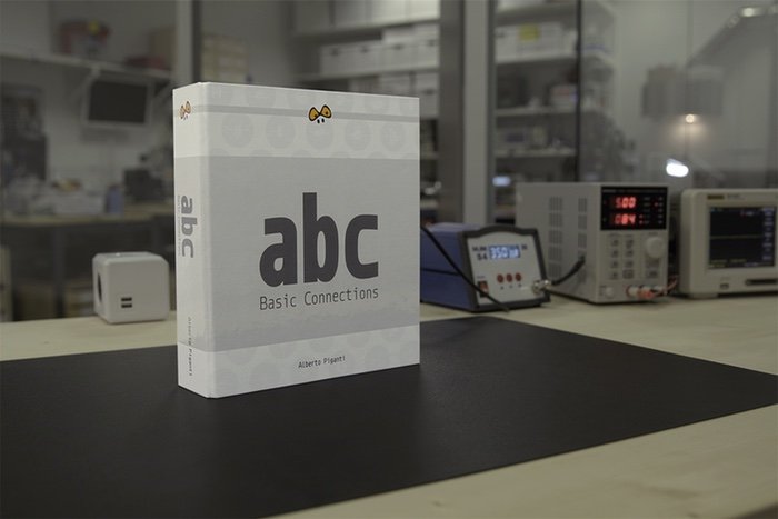
A collection of neat circuit diagrams that shows you how to properly connect almost anything to your Arduino compatible board. Live on kickstarter.
ABC: Basic Connections – The Essential Book for Makers – [Link]
A collection of neat circuit diagrams that shows you how to properly connect almost anything to your Arduino compatible board. Live on kickstarter.
ABC: Basic Connections – The Essential Book for Makers – [Link]
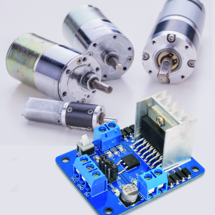
Boris Landoni writes about a new open source project a DC motor controller with control LEDs:
The circuit board we are presenting this time is based on the dual-bridge driver L298N, in a traditionally mounted version in a Multiwatt container with 15 staggered pins; it has two terminal blocks for attaching to DC motors or the coils of a bipolar stepper motor and a terminal block for powering logics and motors. Each of the two output channels of the circuit can provide a maximum current of 2 A, which is enough to drive two 2 A direct current motors or a bipolar stepper motor absorbing 2 A per phase.
A DC Motor Controller with Control Leds – [Link]
Dilshan Jayakody has published a new build:
The current source introduced in this article is capable to handle current up to 6A with maximum input voltage of 50V. This is an operational amplifier based adjustable current source and it uses LM358 in a general voltage follower configuration. To handle large currents we use four 0.1Ω 20W resistors as “load resistor”, and those load resistors are drive through pair of 55N06 N-channel MOSFET transistors.
The power supply unit of this project is build around 9V x 2 (2A) step-down transformer and it is design to get regulated 12V DC voltage. In our design this 12V power source is used to drive LM358 Op-Amp and 12V cooling fan.
Adjustable constant current source – [Link]
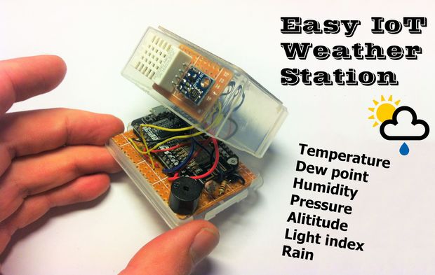
@ instructables.com show us an easy to build IoT weather station able to measure temperature, dew point, humidity, pressure, light index, and rain. He writes:
A weather station is a fun project that teaches you a ton about electronics with the added benefit being an actually useful little device. The project requires a bunch of cheap parts and sensors totaling less than $15, and the whole thing ends up fitting in your hand. The station creates a web site that monitors temperature, dew point, humidity, pressure, light index, and rain (Thingspeak channel). It’s a pretty easy set up, and you’ll just need some basic electronics skills to get it going.
Easy IoT Weather Station With Multiple Sensors – [Link]
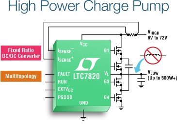
The LTC7820 is a fixed ratio high voltage high power switched capacitor/charge pump controller. The device includes four N-channel MOSFET gate drivers to drive external power MOSFETs in voltage divider, doubler or inverter configurations. The device achieves a 2:1 stepdown ratio from an input voltage as high as 72V, a 1:2 step-up ratio from an input voltage as high as 36V, or a 1:1 inverting ratio from an input voltage up to 36V. Each power MOSFET is switched with 50% duty cycle at a constant pre-programmed switching frequency. System efficiency can be optimized to over 99%. The LTC7820 provides a small and cost effective solution for high power, non-isolated intermediate bus applications with fault protection.
LTC7820 – Fixed Ratio High Power Inductorless (Charge Pump) DC/DC Controller – [Link]
SK Hynix Incorporated introduced the world’s first 72-Layer 256Gb (Gigabit) 3D (Three-Dimensional) NAND Flash based on its TLC (Triple-Level Cell) arrays and own technologies. This company also launched 6-Layer 128Gb 3D NAND chips in April 2016 and has been mass producing 48-Layer 256Gb 3D NAND chips since November 2016. Within 5 months the researchers in SK Hynix developed the new technology of producing 72-layer 3D NAND flash.
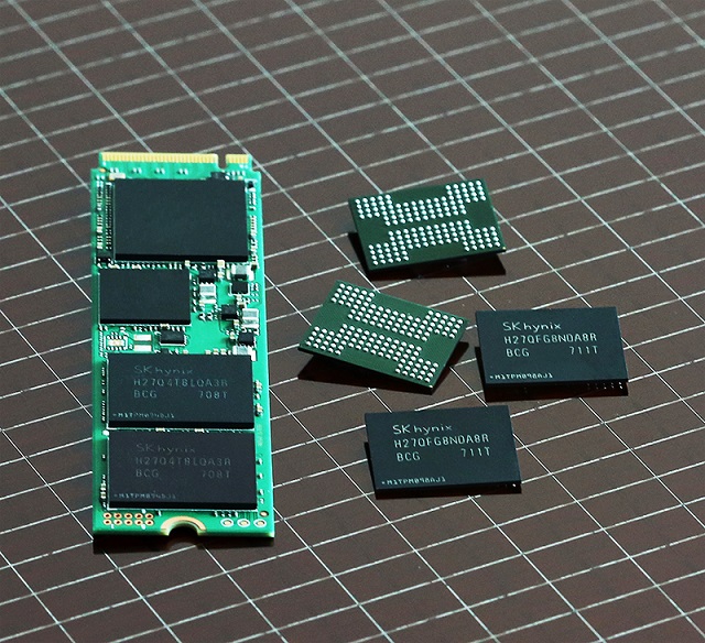
The technological achievement of this 72-Layer 3D NAND is compared to the difficulty of building approximately 4 billion 72-storied skyscrapers on a single dime. Well, now the question maybe, “Is the difficulty and complexity of this new technology giving any remarkable outcome?”. The answer is a big YES. The 72-layer NAND is said to stack 1.5 times more cells than the 48-layer, achieving 30% more efficiency in productivity and 20% higher read/write performance than a 48-layer 3D NAND chip, the predecessor of this 72-layer .D 256Gb NAND flash.
With this new chips having 30% more efficiency in productivity and 20% higher performance, SK Hynix has been currently developing NAND Flash solutions such as SSD (Solid State Drive) and storage for mobile devices such as smartphones. Having high reliability and low power consumption this 3D NAND flash should be an ideal solution for storage problems of mobile devices.
SK Hynix plans to expand the usage of the product to SSDs and mobile gadgets to further improve its business structure weighted towards DRAM. The vice president Jong Ho Kim said in the press release,
With the introduction of this industry’s highest productivity 3D NAND, SK Hynix will mass produce the 256Gb 3D NAND in the second half of this year to provide this to worldwide business clients for optimum use in storage solutions
According to a market research, 3D NAND flash demand is rapidly increasing across AI(Artificial Intelligence), big data, and cloud storage. The research by Gartner says that NAND Flash market revenue is expected to total USD 46.5 billion in this year and it will grow up to an amount of USD 56.5 billion in 2021.
PandwaRF, is a portable low-power RF device that captures, analyses and re-transmits RF signals via an Android device or a Linux PC. It uses Bluetooth (BLE) or USB connection to transmit data in a simple and fast way, comes in the form of a controllable housing from a smartphone or a computer.
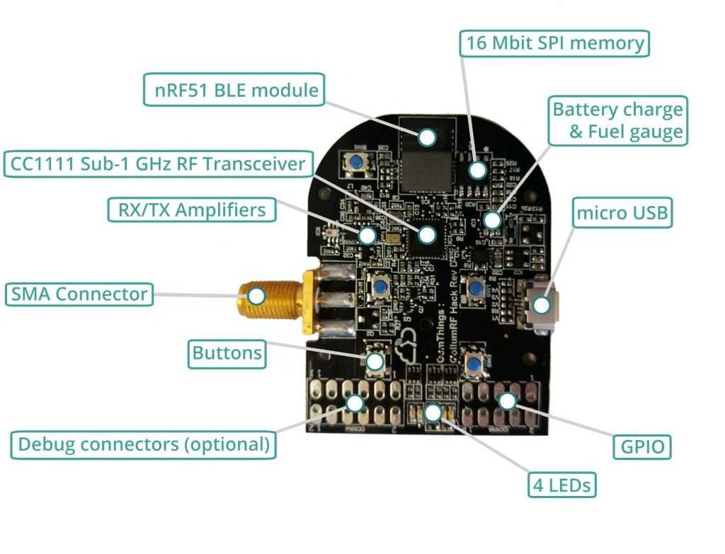
This pocket-size device operates at sub-1 GHz range, and it replaced the ‘standard SDR Grind’ of capturing, demodulating, analyzing, modifying and replaying by hand with a simple powerful interface.
The PandwaRF consists of a capable hardware device, tailored for beginners and advanced users, with an application that runs either on an Android device or on a PC. The Android interface provides full functionality to control and customize the PandwaRF easily using JavaScript.
PandwaRF features are not fully complete yet, the developers had finished captured data processing offload, radio scripting (JavaScript & Python), RF packet sniffer, and spectrum analyzer. Other features are still in development process.
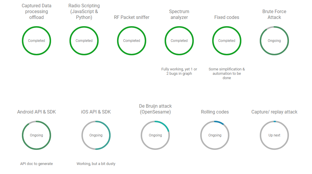
The device is available in three options, the Bare version is about $120 and comes without housing and without battery, the standard version is about $142 with battery and black case, in addition the extended version with enhanced features.
You can reach more information and order your PandwaRF on the official website.
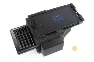
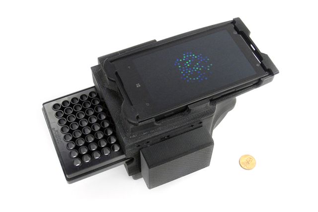
Researchers at UCLA have developed an improved method to detect the presence of DNA biomarkers of disease that is compatible with use outside of a hospital or lab setting. The new technique leverages the sensors and optics of cellphones to read light produced by a new detector dye mixture that reports the presence of DNA molecules with a signal that is more than 10-times brighter.
Nucleic acids, such as DNA or RNA, are used in tests for infectious diseases, genetic disorders, cancer mutations that can be targeted by specific drugs, and fetal abnormality tests. The samples used in standard diagnostic tests typically contain only tiny amounts of a disease’s related nucleic acids. To assist optical detection, clinicians amplify the number of nucleic acids making them easier to find with the fluorescent dyes.
Both the amplification and the optical detection steps have in the past required costly and bulky equipment, largely limiting their use to laboratories.
In a study published online in the journal ACS Nano, researchers from three UCLA entities — the Henry Samueli School of Engineering and Applied Science, the California NanoSystems Institute, and the David Geffen School of Medicine — showed how to take detection out of the lab and for a fraction of the cost.
The collaborative team of researchers included lead author Janay Kong, a UCLA Ph.D. student in bioengineering; Qingshan Wei, a post-doctoral researcher in electrical engineering; Aydogan Ozcan, Chancellor’s Professor of Electrical Engineering and Bioengineering; Dino Di Carlo, professor of bioengineering and mechanical and aerospace engineering; and Omai Garner, assistant professor of pathology and medicine at the David Geffen School of Medicine at UCLA.
The UCLA researchers focused on the challenges with low-cost optical detection. Small changes in light emitted from molecules that associate with DNA, called intercalator dyes, are used to identify DNA amplification, but these dyes are unstable and their changes are too dim for standard cellphone camera sensors.
But the team discovered an additive that stabilized the intercalator dyes and generated a large increase in fluorescent signal above the background light level, enabling the test to be integrated with inexpensive cellphone based detection methods. The combined novel dye/cellphone reader system achieved comparable results to equipment costing tens of thousands of dollars more.
To adapt a cellphone to detect the light produced from dyes associated with amplified DNA while those samples are in standard laboratory containers, such as well plates, the team developed a cost-effective, field-portable fiber optic bundle. The fibers in the bundle routed the signal from each well in the plate to a unique location of the camera sensor area. This handheld reader is able to provide comparable results to standard benchtop readers, but at a fraction of the cost, which the authors suggest is a promising sign that the reader could be applied to other fluorescence-based diagnostic tests.
“Currently nucleic acid amplification tests have issues generating a stable and high signal, which often necessitates the use of calibration dyes and samples which can be limiting for point-of-care use,” Di Carlo said. “The unique dye combination overcomes these issues and is able to generate a thermally stable signal, with a much higher signal to noise ratio. The DNA amplification curves we see look beautiful — without any of the normalization and calibration, which is usually performed, to get to the point that we start at.”
Additionally, the authors emphasized that the dye combinations discovered should be able to be used universally to detect any nucleic acid amplification, allowing for their use in a multitude of other amplification approaches and tests.
The team demonstrated the approach using a process called loop-mediated isothermal amplification, or LAMP, with DNA from lambda phage as the target molecule, as a proof of concept, and now plan to adapt the assay to complex clinical samples and nucleic acids associated with pathogens such as influenza.
The newest demonstration is part of a suite of technologies aimed at democratizing disease diagnosis developed by the UCLA team. Including low-cost optical readout and diagnostics based on consumer-electronic devices, microfluidic-based automation and molecular assays leveraging DNA nanotechnology.
This interdisciplinary work was supported through a team science grant from the National Science Foundation Emerging Frontiers in Research and Innovation program.
Source: UCLA
In serial interface world, there are differential and non-differential protocols. The most famous one of differential interfaces is USB besides HDMI and others, while I2C is a non-differential one.
Joshua Vasquez from Hackaday decided to use DI2C (differential version of I2C) to communicate with a string of BNO055 sensor boards (a smart 9-DOF sensor with I2C interface).
If you’re not familiar with differential communication, the method behind it is straightforward; the line has two channels (positive and negative), where each line has the same signal but with an opposite voltage. The receiver then will calculate the difference between them. Mathematically:
Vb = -Va, So:
Vout = Va – Vb = Va – (-Va)
Now, what if there was a noise?. The noise will affect almost identically on both signals with the same voltage level. As a result the receiver can omit the noise in the output.
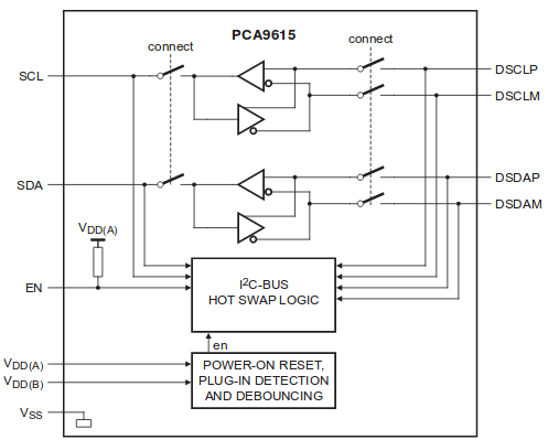
Back to I2C; Joshua used PCA9615 chip from NXP which is a bridge between the normal 2-wire I2C-bus and the 4-wire DI2C-bus.
As an use case; Joshua used DI2C to build an IMU Noodle for modeling a piece of foam twisting and turning in a 3D space simulator using data comes from a string of cards contain the BNO055 sensor and PCA9615 bridge.
PCA9615 was used in each Joshua’s card to bridge the normal I2C signals to DI2C ones. By bridging I2C to DI2C, PCA9615 makes the capability of using longer cables and I2C more rugged in noisy environments.
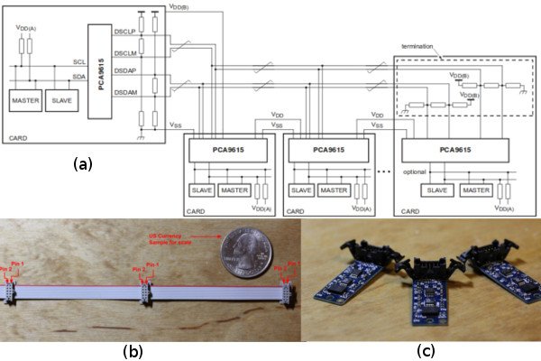
The PCB design files (KiCAD) and firmware can be downloaded from Joshua’s repository on Github. Moreover, Joshua mentioned important tips to setup DI2C in your next design. You can see these tips in his blog post on Hackaday.
Build your own PrivateCloud: Store music & movies, share photo albums with friends, protect your files and never fear losing data again.
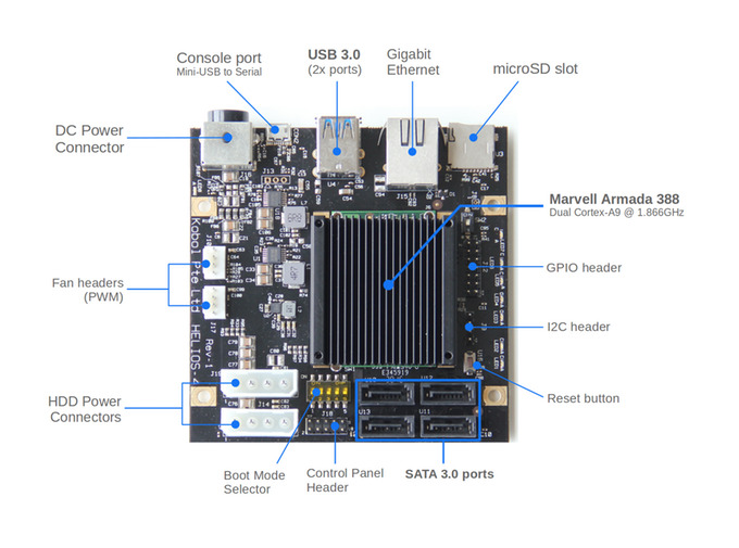
Helios4 is a Network Attached Storage or NAS – a smart box with up to 4 hard drives designed to store Family Photos, Music playlists, and Movie collections by connecting to your Home network.
Helios4 -The World’s 1st Open Source NAS – [Link]