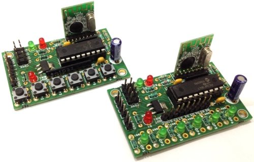
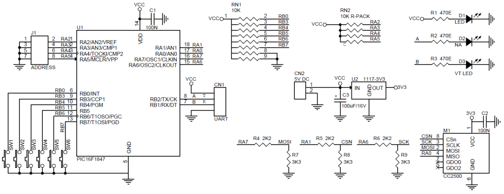
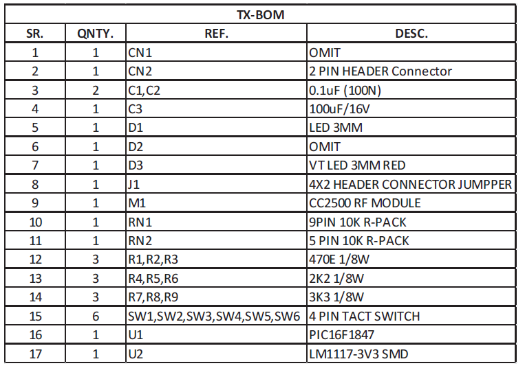
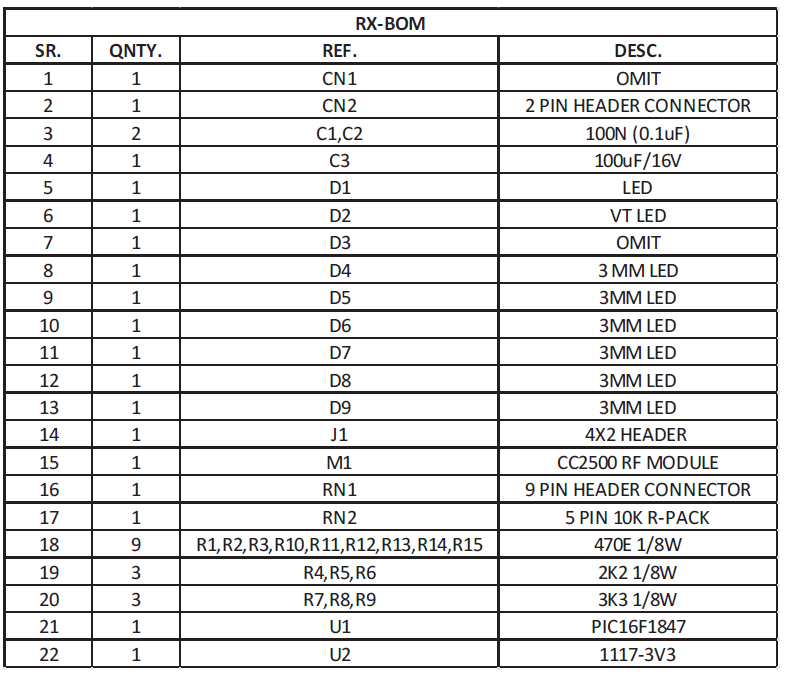
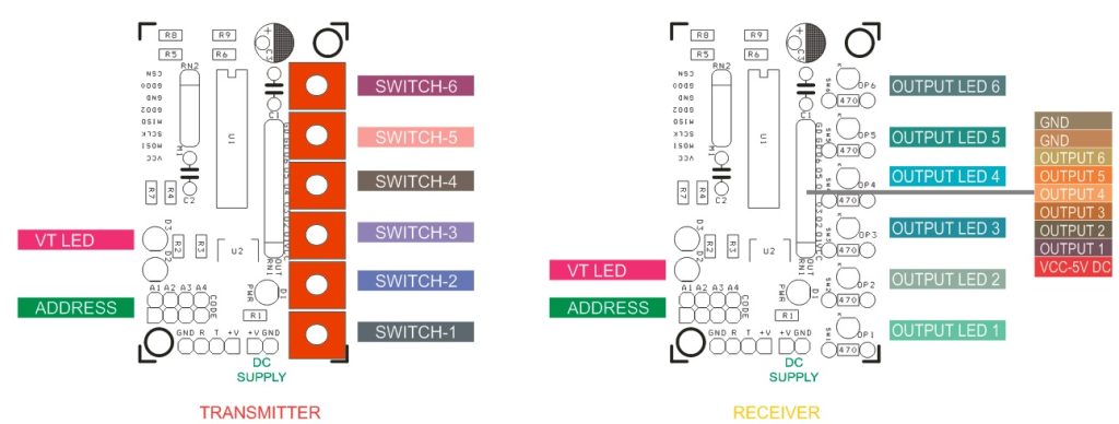
The 6 Channel RF Remote Controller designed using CC2500 RF Transceiver modules and PIC16F1847 micro-controller from microchip. Transmitter provided with 6 tact switch, 4 Address Jumpers to pair multiple unit so they don’t interfere with each other. Board provided with power LED, valid transmission LED. Project works with 5 V DC, On board LM1117-3.3V regulator for CC2500 Module. Two in one PCB can be used as Transmitter & Receiver.
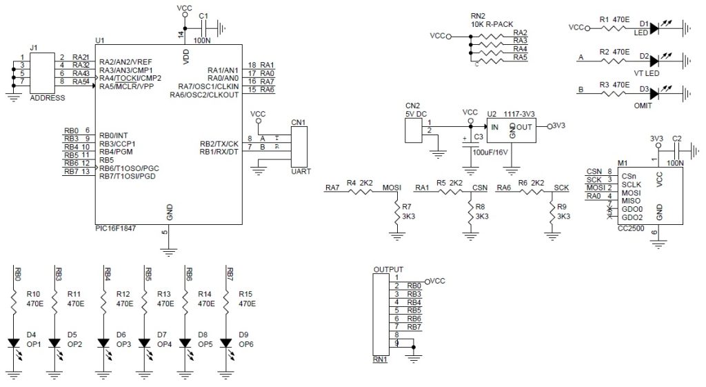
Receiver works with 5V DC. 4 Jumper to paring RX& TX units, valid signal LED, power LED, and 9 Pin connector for outputs. Same PCB is used as transmitter and receiver. All outputs are Latch Type and TTL 5V Signal for easy interface with other devices like Relay Boards, Solid State Relays.
The 6 Channel RF Remote Controller designed using CC2500 RF Transceiver modules and PIC16F1847 micro-controller from microchip. Transmitter provided with 6 tact switch, 4 Address Jumpers to pair multiple unit so they don’t interfere with each other. Board provided with power LED, valid transmission LED. Project works with 5 V DC, On board LM1117-3.3V regulator for CC2500 Module. Two in one PCB can be used as Transmitter & Receiver.
Receiver works with 5V DC. 4 Jumper to paring RX& TX units, valid signal LED, power LED, and 9 Pin connector for outputs. Same PCB is used as transmitter and receiver. All outputs are Latch Type and TTL 5V Signal for easy interface with other devices like Relay Boards, Solid State Relays.
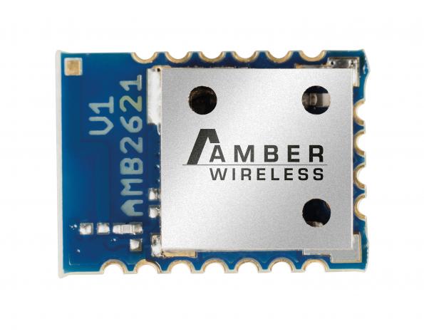
CC2500 RF Module
The CC2500 is a low-cost 2.4 GHz transceiver designed for very low-power wireless applications. The circuit is intended for the 2400-2483.5 MHz ISM (Industrial, Scientific and Medical) and SRD (Short Range Device) frequency band. The RF transceiver is integrated with a highly configurable baseband modem. The modem supports various modulation formats and has a configurable data rate up to 500 baud. CC2500 provides extensive hardware support for packet handling, data buffering, burst transmissions, clear channel assessment, link quality indication and wake-on-radio.
The main operating parameters and the 64-byte transmit/receive FIFOs of CC2500 can be controlled via an SPI interface. In a typical system, the CC2500 will be used together with a microcontroller and a few additional passive components.
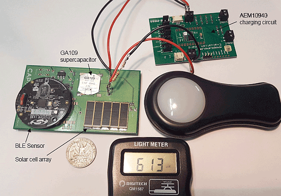
Amber wireless GmbH’s AMB2621 Bluetooth Smart module is a 2.4 GHz BLE wireless module based on the Bluetooth Smart 4.2 standard, measuring only 11x8x1.8mm and offered with or without integrated antenna.
Bluetooth Smart module is only 11x8x1.8mm – [Link]
In Part 1 of this series, we have reviewed solar cell performance, how to select and size the supercapacitor, requirements of supercapacitor charging circuits and charging IC characteristics. We will now use two case studies to illustrate these properties in detail.
Using a supercapacitor for power management and energy storage with a small solar cell – [Link]
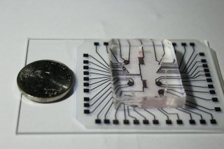
Researchers at the Stanford University School of Medicine have developed a way to produce a cheap and reusable diagnostic “lab on a chip” with the help of an ordinary inkjet printer. At a production cost of as little as 1 cent per chip, the new combination of microfluidics, electronics and inkjet printing technology could usher in a medical diagnostics revolution like the kind brought on by low-cost genome sequencing, said Ron Davis, PhD, professor of biochemistry and of genetics and director of the Stanford Genome Technology Center.
Lab on a Chip – Zahra Koochak
The lab on a chip consists of two parts: a clear silicone microfluidic chamber for housing cells and a reusable electronic strip and a regular inkjet printer that can be used to print the electronic strip onto a flexible sheet of polyester using commercially available conductive nano-particle ink.
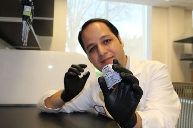
“Enabling early detection of diseases is one of the greatest opportunities we have for developing effective treatments,” Rahim Esfandyarpour said, a PhD and an engineering research associate at the genome center. “Maybe $1 in the U.S. doesn’t count that much, but somewhere in the developing world, it’s a lot of money.”
Designed as a multi-functional platform, one of its applications is that it allows users to analyse different cell types without using fluorescent or magnetic labels that are typically required to track cells. Instead, the chip separates cells based on their intrinsic electrical properties:
When an electric potential is applied across the inkjet-printed strip, cells loaded into the microfluidic chamber get pulled in different directions depending on their “polarisability” in a process called dielectrophoresis. This label-free method to analyse cells greatly improves precision and cuts lengthy labeling processes.
Rahim Esfandyarpour helped to develop a way to create a diagnostic “lab on a chip” for just a penny. Zahra Koochak
The tool is designed to handle small-volume samples for a variety of assays. The researchers showed the device can help capture single cells from a mix, isolate rare cells and count cells based on cell types.The low cost of the chips could democratize diagnostics similar to how low-cost sequencing created a revolution in health care and personalized medicine, Davis said. Inexpensive sequencing technology allows clinicians to sequence tumor DNA to identify specific mutations and recommend personalized treatment plans. In the same way, the lab on a chip has the potential to diagnose cancer early by detecting tumor cells that circulate in the bloodstream.
Since Autodesk acquired Eagle CAD, big changes have been made to Eagle CAD. Regardless of the new licensing system using subscription model, which was a subject to criticism by a lot of users, the new management of Eagle from Autodesk has successfully added a lot of demanding features that old team failed to bring out.
Eagle 8 came with a lot of new features like BGA auto-router and “Past Block Design” tool to add a complete block of connected components both in schematic and board.
The new release 8.1.1 brought PCB alignment tool to align a group of objects in different positions; top, bottom, left, right, center, and distribute horizontally / distribute vertically.
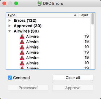
Another improvement in eagle 8.1.1 that deserves mention is that a new category has been added to DRC (Design Rule Check) called Airewire. It’s an important improvement because airwires is one of the most common things designer should be aware of. In older Eagle releases, you should work with your eyes wide open and never forget to hit ratsnest at the end of your work and read the magic sentence in the bottom corner “Ratsnest: Nothing to do !”.
Fritz Weld @ edn.com proposes a simple circuit to check li-ion battery health. He writes:
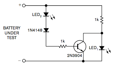
Lithium-ion batteries are sensitive to bad treatment. Fire, explosions, and other hazardous condition may occur when you charge the cell below the margin that the manufacturer defines. Modern battery chargers can manage the hazardous conditions and deny operation when illegal situations occur. This fact doesn’t mean, however, that all cells are bad. In most cases, you can replace the discharged battery and increase your device’s lifetime. Figure 1 shows the circuit for testing battery packs.
Simple circuit indicates health of lithium-ion batteries – [Link]
Welcome to the 6th post of the “Exploring Eagle CAD ULPs” series. Each post will be discussing one useful ULP in Eagle CAD.
“ULP” User Language Program is a plain text file which is written in a C-like syntax and can be used to access the EAGLE data structures and to create a wide variety of output files. You can think about it as a plug-in for Eagle.
You can reach the posts published in this series using the following link.
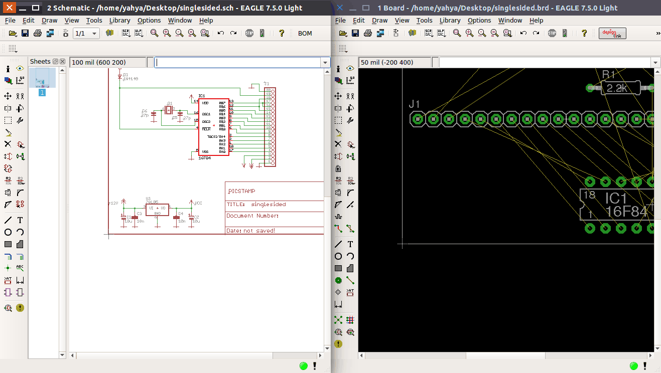
In the previous post we explored Place50 ULP which places all parts of the board to the position in the schematic. Place50 moves all parts of the board, but sometimes we need to do this auto-placement for just a certain group of parts. Beside that, we can’t change the position scaling factor in Place50. Group-aps_v4 ULP overcomes these two points of limitation in Place50 ULP by doing the auto-placement by group, and having user defined position scaling and offset.
To use Group-aps_v4 ULP first download it from Autodesk website. Before running it in the schematic editor, you need to define a group of parts first.
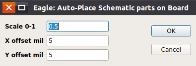
Group-aps_v4 has a simple dialog to enter scale and offset values.
Scale is used to scale the value of original position (X and Y) of the parts in the defined group in the schematic. While X,Y offset is used to offset the final position of the part in the board after scaling it. For example, if scale was 0.5 and the position (in mil) for the part is (500,100) then is will be considered as (250,50).
Group-aps_v4 ULP originally places the group in the calculated position of the the first part. So as an output, all parts will have the same X and Y and that’s not effective. So i made a simple edit to the ULP to solve this issue. You can download the updated version N_group-aps_v4.ulp.
Compressed sensing is an new computational technique to extract large amounts of information from a signal. Researchers from Rice University, for example, have built a camera that can generate 2D-images using only a single light sensor (‘pixel’) instead of the millions of pixels in the sensor of a conventional camera.
This compressed sensing technology is rather inefficient for forming images: such a single-pixel camera needs to take thousands of pictures to produce a single, reasonably sharp image. Researchers from the MIT Media Lab however, have developed a new technique that makes image acquisition using compressed sensing fifty times more efficient. In the example of the single-pixel camera that means that the number of exposures can be reduces to several tens.
One intriguing aspect of compressed sensing is that no lens is required – again in contrast with a conventional camera. That makes this technique also particularly interesting for applications at wavelengths outside of the visible spectrum.
In compressed sensing, use is made of the time differences between the reflected light waves from the object to be imaged. In addition, the light that strikes the sensor has a pattern – as if it passed through a checkerboard with irregular positioned transparent and opaque fields. This could be obtained with a filter or using a micro-mirror array where some mirrors are directed towards the sensor and others are not.
The sensor each time measures only the cumulative intensity of the incoming light. But when this measurement is repeated often enough, each time with a different pattern, then the software can derive the intensity of the light that is reflected from different points of the subject.