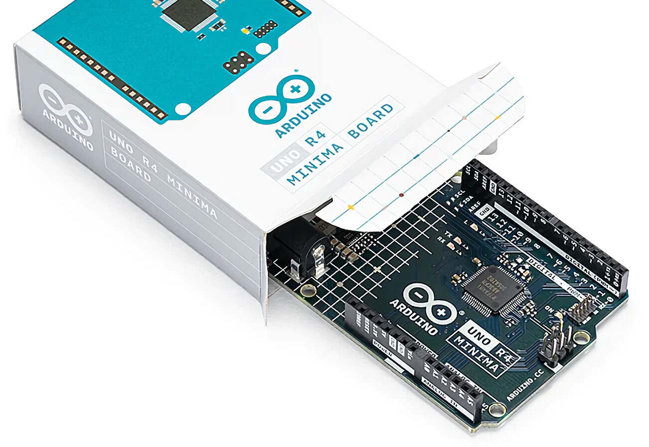
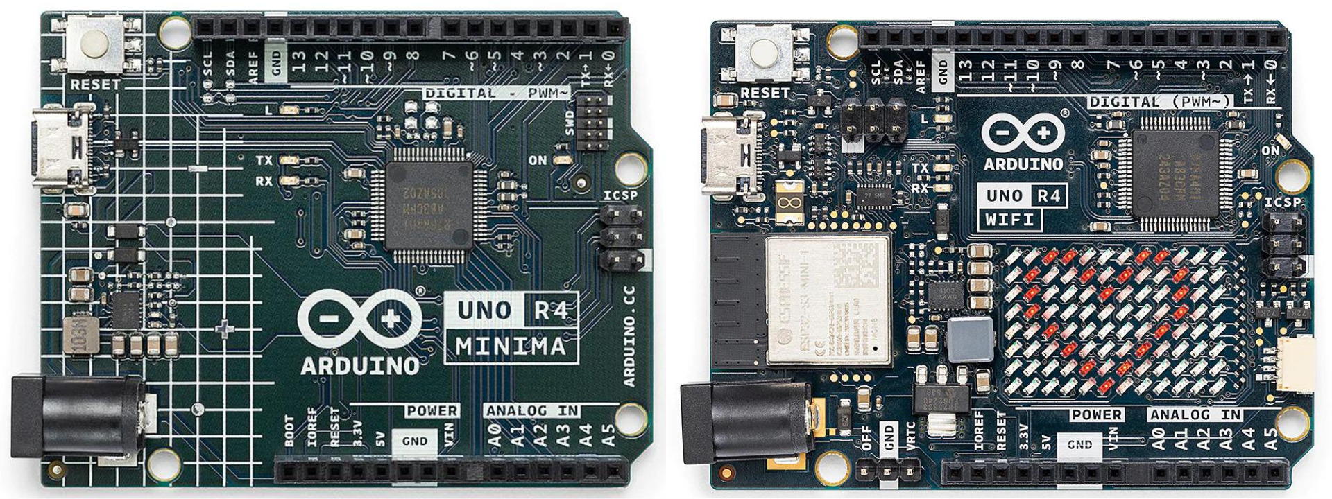
The Arduino Uno has been the “go-to” board for beginners for its simplicity and versatility as it makes a great choice for professionals to develop a proof of concept for their target use cases. Continuing the legacy, Arduino has recently announced the Arduino Uno R4 Minima and R4 Wi-Fi, the successor to the Arduino Uno R3.
While the R4 Minima is a generational upgrade to the R3’s overall power and features, the R4 Wi-Fi adds the features of Wi-Fi communication and a matrix display to the R4 Minima for IoT application implementation.
Technical Specifications of the R4 and R4 Wi-Fi
The 32-bit RA4M1 microprocessor, 32 kB of quicker RAM, and 256 kB of faster Flash memory are all included in the Arduino Uno R4 Minima. The R4 Minima keeps the same amount of PWM-enabled digital I/O pins and analog input pins.
Additionally, the R4 Minima includes a 12-bit DAC, CAN Bus, and an OP-AMP, which are upgrades for customers seeking greater adaptability in the same R3-compatible design. The inclusion of the CAN Bus is particularly beneficial for Internet of Things applications since it permits connecting to other devices in the network – without a host device.
Through the barrel jack connector, the R4 Minima improves the power specifications of its predecessor by supporting a voltage range of 6V to 24V. The seamless connectivity of relatively high-power equipment like motors, LED strips, etc. is made possible thanks to this. In order to continue working with older devices, the R4 Minima core’s operating voltage is 5V. Additionally, Arduino has added the traditional 5V and 3.3V power connectors for compatibility and relevant applications.
R4 Wi-Fi Adds More to the R4 Minima
Using the ESP32-S3, which operates at 240 MHz and 3.3 V, the R4 Wi-Fi combines all the functionality of the R4 Minima, and it adds many more features. With a separate 384 KB of ROM and 512 KB of SRAM, this microcontroller equips the R4 Minima with Wi-Fi, Bluetooth, and BLE networking features.
The ESP32-S3 microcontroller provides AI acceleration through vector calculation instructions, making the R4 Wi-Fi a reliable AIoT device if these characteristics weren’t enough. Moreover, the inclusion of the 12 x 8 matrix display is a key addition to the utility of the IoT functions enabled by the R4 Wi-Fi.
Software and IoT Integration of Arduino Uno R4
The Arduino family of devices has become a solid platform for the development of projects because of its IDE features and easy-to-use programming language.
With the addition of the SWD debugging port, native support for the Qwiic ecosystem of devices, HID device support, and wireless connectivity, the R4 Wi-Fi aims to amplify the abilities of the platform and become a universal option for microcontroller-based projects for beginners and professionals alike. Additionally, the AI-accelerated vector instructions help in the execution of repeated tasks much faster than normal processing to reduce latency and give a much more responsive human interaction experience.
Despite developing such a formidable platform for IoT, Arduino has attempted to take things further by announcing an online API service named Arduino IoT Cloud. The service enables users to code, visualize, monitor, and debug IoT-connected Arduino devices remotely and without achieving much expertise in wireless communication systems and protocols.
On a conclusive note, Arduino has a very strong portfolio of microcontrollers. The addition of processing power, IoT support and various other features to the R4 Minima and R4 Wi-Fi give Arduino a wider sense of appeal as a universal platform for beginners and professionals alike.
The Arduino Uno R4 Minima and R4 Wi-Fi are on sale for $20.oo and $27.50, respectively. For more information, visit the official product pages of Uno R4 Minima and Uno R4 Wi-Fi.
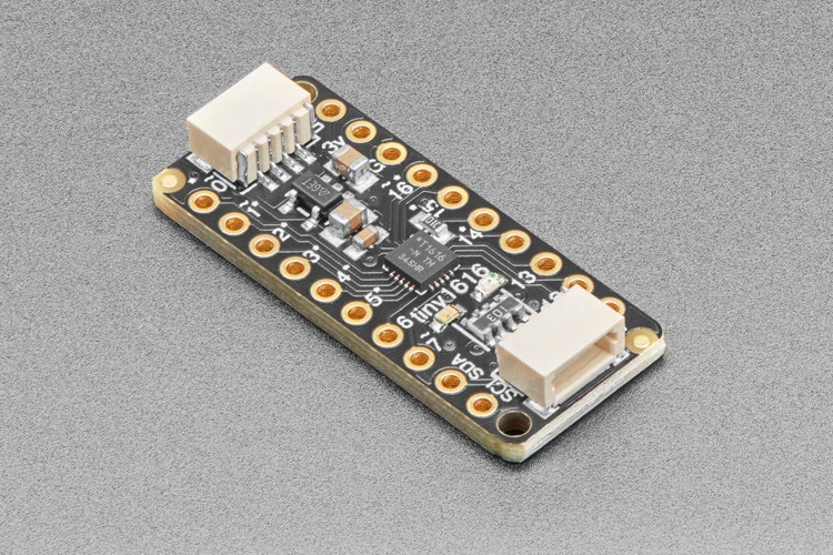
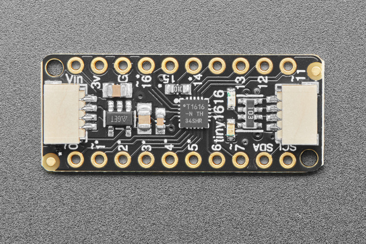
Adafruit’s latest ATtiny1616-basedbreakoutboard is slightly more unique than the average breakout board you can commonly find in the market. Not only this board features the SeesawFirmware, but it also features the STEMMAQT/ Qwiic connector, through which you can use this board as a plug-and-play I2C controller or peripheral.
So, why would you need a separate microcontroller as an I2C peripheral? Does the main microcontroller already have all the necessary functionality? Well, it all depends on the project requirements. Sometimes, you may need additional GPIOs; sometimes, there could be a need for extra ADC. In other cases, there could be a situation where strict timing requirements need to meet for a peripheral to work.
When discussing strict timing requirements, the WS2812B is a great example. The LEDs will only light up if the timing is managed correctly. Speaking of Neopixel, this board is perfect for driving Neopixel LEDs because it has a dedicated Neopixel driver capable of driving up to 250 LEDs.
So, having an I2C expansion board on top of your microcontroller is cool and all, but doesn’t make the coding part more complicated? Well, it turns out that Adafrut is also taking care of that by giving us custom software libraries for Arduino and Python which is the two most used embedded development platforms.
The seesaw firmware runs on a microcontroller, like Microchip’s ATtiny1616 breakout board, and handles all the communication processes, the ATtiny1616 comes preloaded with the seesaw firmware and you have custom libraries available for Arduino and Python. The code is pretty simple, here is an example code for setting up PWM on the ATTiny1616 breakout board:
# SPDX-FileCopyrightText: 2021 ladyada for Adafruit Industries
# SPDX-License-Identifier: MIT

# Simple seesaw test for writing PWM outputs
# On the SAMD09 breakout these are pins 5, 6, and 7
# On the ATtiny8x7 breakout these are pins 0, 1, 9, 12, 13
#
# See the seesaw Learn Guide for wiring details.
# For SAMD09:
# https://learn.adafruit.com/adafruit-seesaw-atsamd09-breakout?view=all#circuitpython-wiring-and-test
# For ATtiny8x7:
# https://learn.adafruit.com/adafruit-attiny817-seesaw/pwmout

import time
import board
from adafruit_seesaw import seesaw, pwmout

i2c = board.I2C()  # uses board.SCL and board.SDA
# i2c = board.STEMMA_I2C()  # For using the built-in STEMMA QT connector on a microcontroller
ss = seesaw.Seesaw(i2c)

PWM_PIN = 12  # If desired, change to any valid PWM output!
led = pwmout.PWMOut(ss, PWM_PIN)

delay = 0.01
while True:
    # The API PWM range is 0 to 65535, but we increment by 256 since our
    # resolution is often only 8 bits underneath
    for cycle in range(0, 65535, 256):  #
        led.duty_cycle = cycle
        time.sleep(delay)
    for cycle in range(65534, 0, -256):
        led.duty_cycle = cycle
        time.sleep(delay)
The example code is taken from Adafruit’s website and you can check that out for more information.
The Adafruit ATtiny1616 breakout is interesting because it uses Microchip’s new family of microcontrollers the ATtiny1616. Despite its compact size, it offers 16 kilobytes of flash memory, 2 kilobytes of RAM, and 256 bytes of program-accessible EEPROM. Furthermore, it features an internal oscillator clocked at 20 MHz.
By default, the breakout board operates at 5V, but the operating voltage range of the ATtiny1616 microcontroller is between 2V to 5V. That is why there is a 3.3v regulator onboard; the regulator provides flexibility allowing seamless interfacing with 3.3V devices.
Features of the Adafruit ATtiny1616 Breakout Board
The ATtiny1616 breakout board from Adafruit offers many features designed to extend the capabilities of microcontrollers. Here are the key specifications:
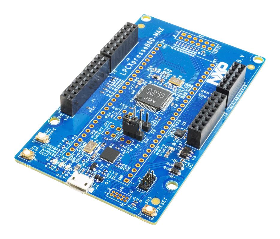
NXP, a leading semiconductor manufacturer, has recently announced its new evaluation board with the LPC86x processor. This evaluation board features the LPC860-MAX chip, which includes a 32-bit ultra-low-power Arm Cortex-M0 processor which has 54 GPIO pins. With a net cost of $15, this board supports a range of moderate to lightweight applications such as Battery Management Systems(BMS), Building Safety, Motor Drives, Smart Lighting, Smart Speakers, and more.
This new development board features the LPC860-max at its core. With a maximum clock speed of 60MHz, the Cortex-M0 processor offers impressive processing capabilities and a fast single-cycle I/O port. Additionally, this processor provides 64kB of Flash memory and 8kB of RAM, ensuring sufficient storage and computational power for a wide range of applications.
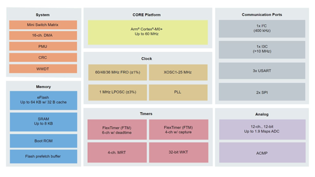
Specifications of the NXP LPC860-MAX Microcontroller
32-bit Arm Cortex-M0+ processor with 60MHz Clock
Single-cycle multiplier and fast single-cycle I/O port
6-channel FlexTimer with motor fault control
4-channel FlexTimer with quadrature encoder
64kB flash memory with 8kB RAM
Windowed Watchdog Timer (WWDT)
Self-Wake-up Timer (SWT)
1x comparator with 5 inputs and internal/external reference voltage
1x DMA with 16 channels and 13 trigger inputs
1x 12-bit ADC (Analog-to-Digital converter)
3x USART , 2x SPI and 1x I2C
1x I3C port (a mid-speed alternative to SPI and compatible with I2C)
Supported by NXP’s software and tools
Compatible with Keil MDK IAR EWARM development environments
Equipped with up to 54x GPIOs (General Purpose Input/Output pins)
Looking at connectivity, this evaluation board offers a wide range of options. It includes a Comparator with five inputs and support for internal/external reference voltages. The board also features a 16-channel DMA with13 trigger inputs, which further enhances its data transfer capabilities. other than that it has, a 12-bit ADC, 3 USART, 2 SPI, 1 I2C, and 1 I3C (>10MHz) providing developers with multiple communication interfaces to suit their specific requirements.
To simplify the development process, NXP support for the LPC860-MAX evaluation board through its MCUXpresso Software and Tools. These software development tools offer a development environment for programming Kinetis, LPC, and i. MX RTmicrocontrollers. The MCUXpresso SDK also provides project files for Keil,MDK, and IAR EWARM, offering flexibility to developers who prefer these development environments.
With NXP’s commitment to providing innovative solutions for the embedded systems market, the LPC860-MAX evaluation board empowers developers to unlock new possibilities and deliver cutting-edge products to consumers across various industries.
In the previous parts of the article, we considered how to convert an analog signal to digital by PCM method, as a binary encoding process. Now we want to consider the reverse process as binary decoding. This combination of binary encoding/decoding procedures is an essential part of signal processing in thousands of applications in the industry and the world of technology.
The purpose of digital-to-analog conversion is to take discrete numerical data (which represent an analog signal) as the input and reproduce the original continuous waveform as the output. Digital-to-analog converters (DACs) are used in transforming digital processing data, back to ‘real-world’ values for further analog processing.
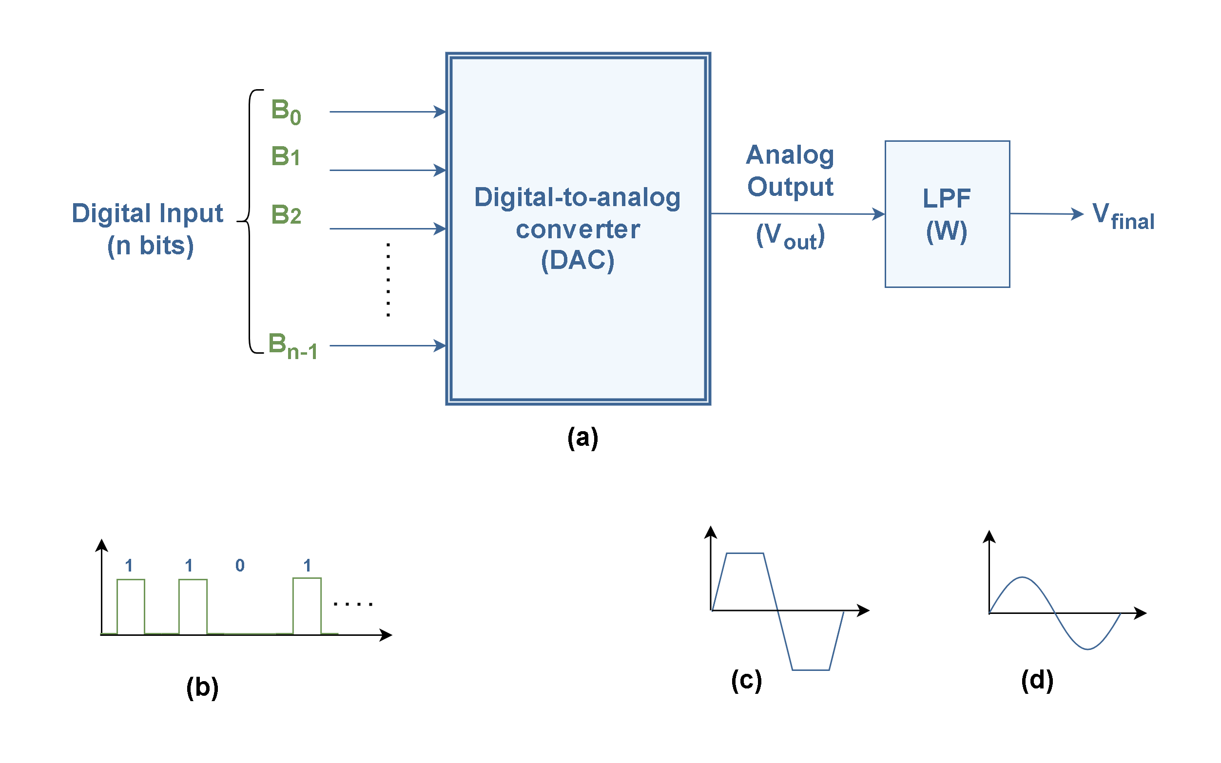
Digital-to-analog converters actually perform the role of re-constructing the original continuous electrical waveform. Since DACs in their configuration are much simpler than ADCs (analog-to-digital converters), they are correspondingly cheaper. Figure 1 shows the schematic of an n-bit DAC.
Figure 1: (a) An n-bit DAC with an LPF after the output terminal (b) Digital waveform at the input (c) Unfiltered analog waveform at the output (Vout) (d) Filtered analog waveform (Vfinal)
Figure 1 (a) shows the main function of an n-bit DAC system to convert binary words [Bn-1 … B1B0] to analog signals at the output (Vout). The typical input waveform is plotted in Figure 1 (b). Although the output analog signals are usually not perfectly reconstructed, as it shown in the typical waveform in Figure 1 (c), a low pass filter (LPF) is almost always necessary to correct the final waveform to be more similar to the original, as shown in Figure 1 (d).
Reconstruction Of The Original Continuous Signal
There are many applications that require the construction of analog waveforms from the digital sequence of numbers. The most common digital-to-analog converter is multiplying DACs. The name arises because the output is constructed by summation of the products of the binary code values and voltage sources. Each bit of the binary code turns on or off a corresponding voltage source. The sum of all the available voltages produces a resultant voltage for output.
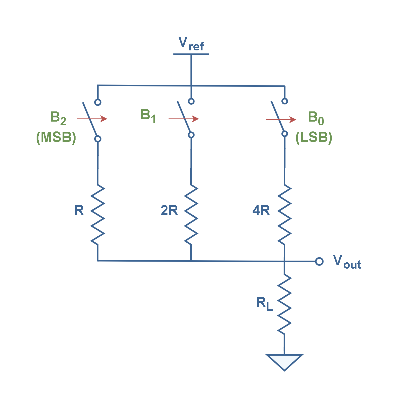
For this purpose, simple resistive networks can be used. Figure 2 shows the concept of converting a three-bit digital input into an analog output by such a resistive network. The resistors are scaled specifically to represent weights for the different input bits. The bits are assumed as electronic switches which may close the circuit while their values are ‘1’ and may also open branches while their values are ‘0’.
Figure 2: Weighted resistive circuit for 3-bit digital to analog conversion
Figure 2 shows the network with a main voltage source (Vref) and three voltage dividers. With the help of simple circuit analysis, like Millman’s theorem, it can be proved that the output voltage is given by Equation 1.
Equation 1: Calculation of the output voltage for the 3-bit weighted resistive DAC
In this expression, B0, B1, and B2 are numerical values of input bits which may be 0 or 1. This expression can be simplified to Equation 2.
Equation 2: The output voltage of the 3-bit weighted resistive circuit
It can be further expressed by considering the weight of bits as Equation 3.
Equation 3: The output voltage of the 3-bit weighted resistive circuit
Thus, Vout is a voltage waveform as the counterpart of the digital word of [B2 B1 B0] at the time of exiting this word (T).
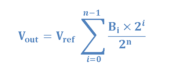
The configuration in Figure 2 can be extended to an n-bit weighted resistive D/A converter to get the following generalized expression in Equation 4.
Equation 4: Generalized calculation of the output voltage for an n-bit weighted resistive DAC circuit
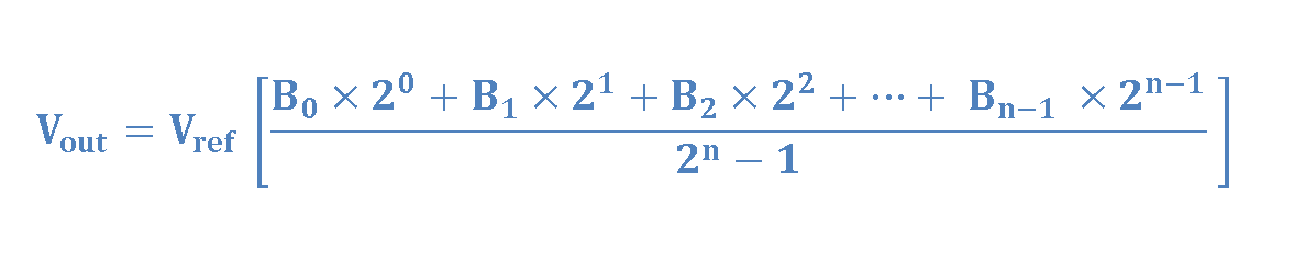
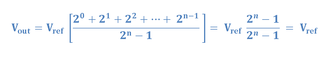
According to Equation 4, a logic ‘1’ at LSB (the least significant bit) position (B0) would contribute Vref /(2n −1) to the output voltage. The contributions of successive higher bit positions in the case of a logic ‘1’ would be 4Vref /(2n −1), 8Vref /(2n −1), and so on. Finally, a logic ‘1’ in MSB (the most significant bit) position would deliver (2n-1. Vref )/(2n −1) to the output, as the most contribution.
When all input bit positions have a logic ‘1’, the maximum analog output is given by Equation 5.
Equation 5: Maximum value of Vout for the n-bit weighted resistive circuit
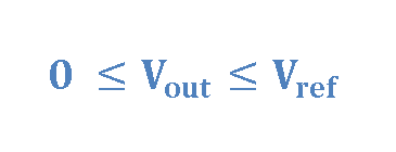
In the case of all inputs being in the logic ‘0’ state, Vout = 0. Therefore, the analog output Vout of the resistive DAC varies from 0 to Vref volts as the digital input varies from an all 0s to an all 1s input. Equation 6 explains the range of the output amplitude Vout .
Equation 6: The minimum and maximum ranges of Vout
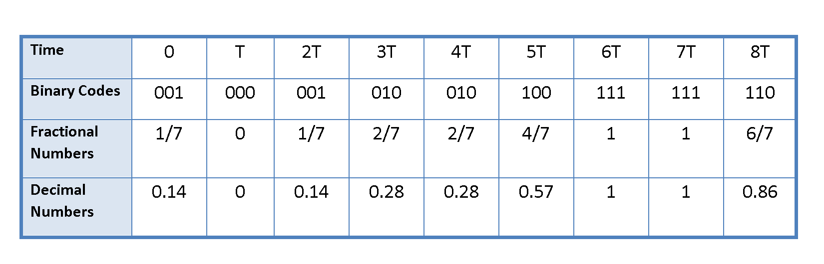
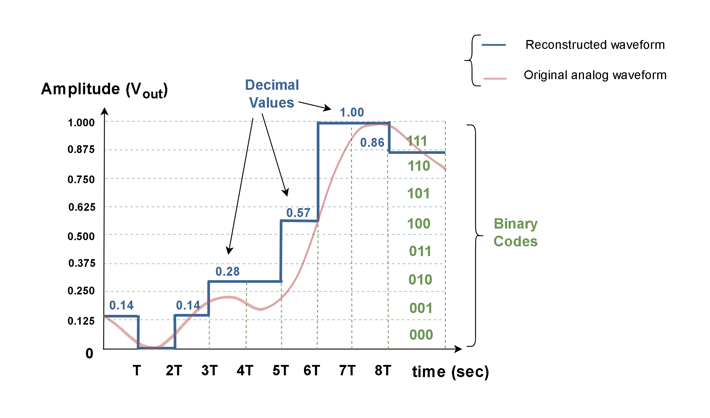
Let’s recall our previous example in the second part of the article:
If we take the results of the ADC conversion in that example as our new input binary data and apply the weighted resistive D/A converter to that binary numbers, the new decimal values result in Table 1 (Vref = 1 V).
Table 1: The decimal output results of DAC corresponding to the digital codes from the previous example
If we plot the results of Table 1 in terms of time, the original analog waveform is reconstructed approximately as shown in Figure 3.
Figure 3: Reconstructed analog waveform by the 3-bit weighted resistive DAC
Obviously, this approximation of the original waveform is not perfect! As we have already considered, the precise conversion of analog waveforms to digital (or from digital domain to analog) needs a large number of bits (3-bit words are normally not enough). A better approximation will be achieved by increasing the number of bits (n).
Also, this waveform is before the stage of filtering. To achieve a smoother curve, an LPF is applied after the output in practical DAC systems.
Weighted-Resistor Network For D/A Conversion
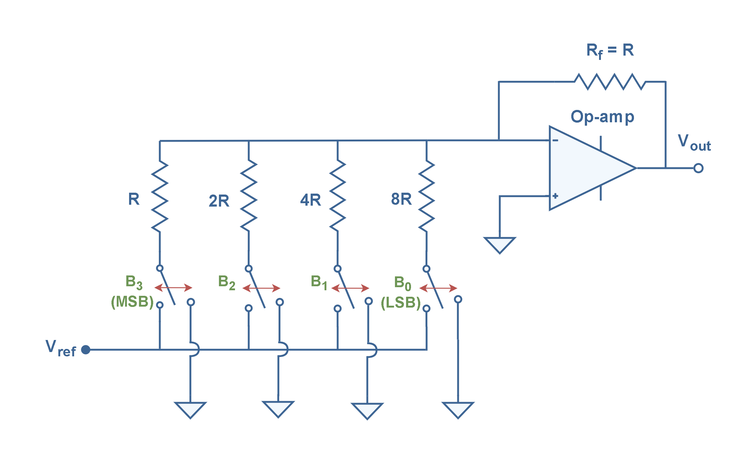
Based on the prior resistive DAC concept, Figure 4 shows a more realistic configuration for a DAC circuit utilizing an operational amplifier.
Figure 4: A 4-bit weighted resistive DAC with a summing amplifier
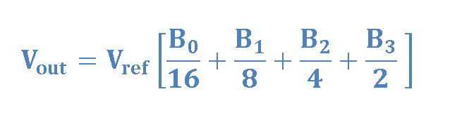
Essentially, this configuration is a weighted-resistor decoder that converts a 4-bit code from digital to analog. The values of resistors are chosen such that the resistance in each branch is double the previous one, i.e. the current reduces by a factor of 2 for each branch or bit path. This arrangement confirms a proper conversion from a binary number to a decimal value. The overall circuit simultaneously uses the ideas of a summing amplifier and an inverting amplifier, with the output voltage Vout.
The voltage source (Vref), as the reference of logic ‘1’ or ‘on’, is applied to a series of scaled resistors. The voltages at one end of the resistors are either switched ‘on’ or ‘off’ relating to the status of input bits as shown in Figure 4. The ‘off’ voltages are grounded to zero and the ‘on’ voltages are summed. The output is proportional to the weighted sum of the input voltages.
The resistor with the lowest value R corresponds to the highest weighted binary input B3 (MSB) with a weight of 23 (= 8). The other resistors with values of 2R, 4R, and 8R respectively correspond to the binary weights of 22 (B2) and 21 (B1), and 20 (B0 which is LSB).
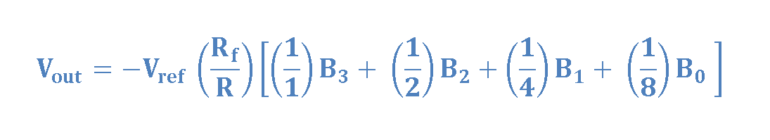
The relationship between the digital input sequence [B3 B2 B1 B0] and the analog output Vout is as Equation 7.
Equation 7: Calculation of Vout for a 4-bit DAC Converter with a summing amplifier
If Vref is originally selected by negative polarity, the positive Vout will be achieved. Some DAC devices have a built-in reference voltage source. Other ones allow the user to provide an external reference voltage, thereby setting the accuracy of the output.
Binary Ladder Network For D/A Conversion
The simple resistive decoder concept of Figure 2 has two serious practical disadvantages:
Each resistor in this network has a different value. Specifically, there is a large difference in resistor values between the LSB and MSB for a large number of bits (n). Such networks usually use precision resistors. Precision resistors are designed for applications where fitted resistance tolerance and stability are primary considerations. Therefore, such a configuration causes extra expenses.
The resistor used for the most significant bit (MSB) is required to handle a much larger current than the LSB resistor. So, for a larger number of bits, we need a set of resistors with different sizes and current characteristics.
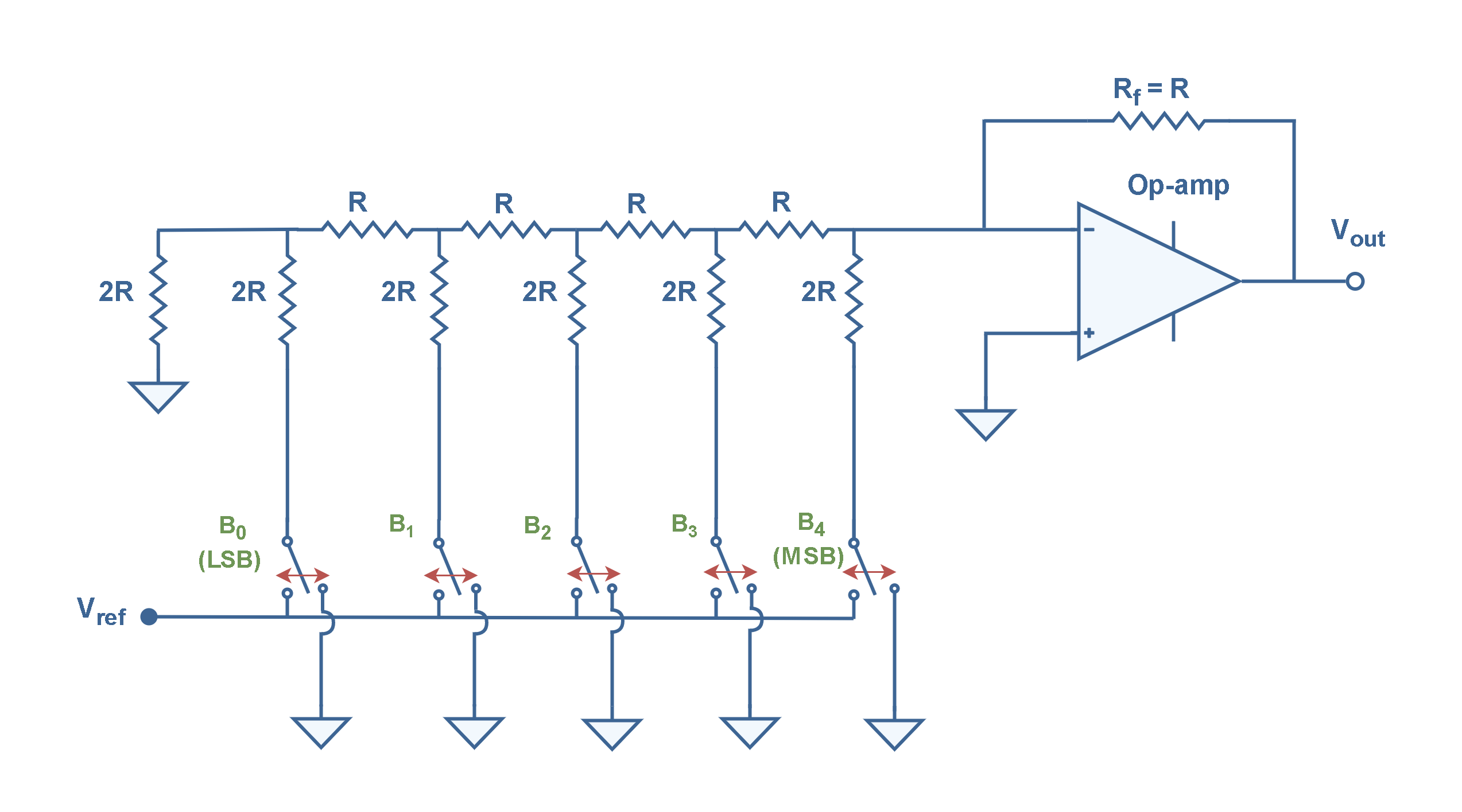
To overcome these disadvantages, a second type of resistive network called the binary ladder (or R/2R ladder) is used in practice. The binary ladder is also a resistive network that produces an analog output equal to the weighted sum of digital inputs. Here the resistance values span a range of only 2 to 1.
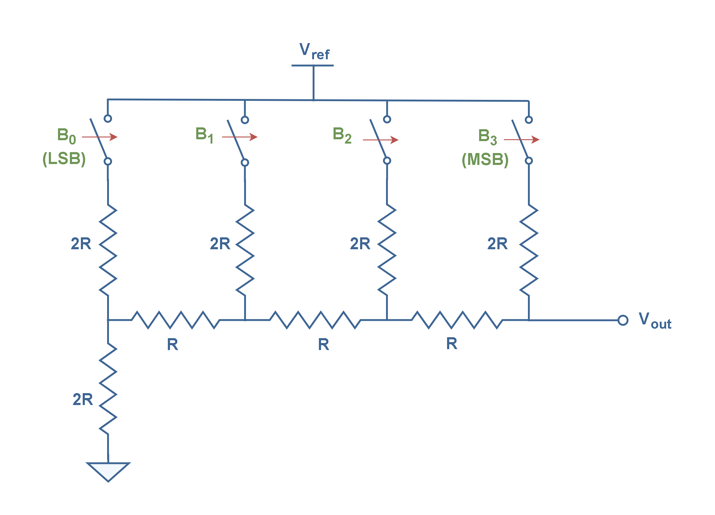
Figure 5 describes the concept of the basic R/2R binary ladder network for a four-bit D/A converter.
Figure 5: R/2R binary ladder resistive circuit for digital-to-analog conversion
The “ladder” description comes from the ladder-like topology of the network. This configuration operates as an array of voltage dividers whose output accuracy is exclusively dependent on how well each resistor is matched to the others.
Note that the network consists of only two resistor values; R and 2R (twice the value of R) no matter how many bits make up the ladder. For this reason, the R/2R ladder is inexpensive and relatively easy to manufacture. All bits pass through resistance of 2R. The less weighty the bit, the more resistors the signal must pass through before reaching the output.
The digital inputs or bits range from LSB (B0) to MSB (B3). The bits are switched between 0 Volt and Vref and each binary input adds its own weighted contribution to the analog output Vout depending on the state and position of the bit. The MSB causes the greatest effect in output voltage and the LSB causes the smallest.
By methodical application of Thevenin’s Equivalent circuits and Superposition Principle, it is possible to analyze the R-2R circuit. With the help of simple mathematics, it can be proved that the analog output voltage Vout in the case of binary ladder network of Figure 5 is given by Equation 8.
Equation 8: Analog output voltage of the binary ladder network (R/2R)
This configuration is easily extendable. Equation 9 explains how to calculate the analog output voltage Vout for a ladder network with n bits.
Equation 9: Calculation of Vout for an n-bit R/2R binary (R/2R) ladder
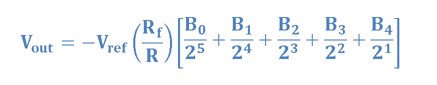
Figure 6 shows a more practical implementation of the R/2R resistor ladder network as a digital-to-analog converter using an op-amp as an inverting summing amplifier.
Figure 6: A 5-bit R/2R DAC with an op-amp summing amplifier
This type of DAC is also known as a multiplying converter. The output voltage is linearly proportional to the digital input states and the range can be adjusted by changing the reference voltage Vref. The Thevenin resistance of an R/2R ladder is always R –regardless of the number of bits in the ladder. Therefore, in this configuration, the source impedance as seen by the op-amp is always constant and equal to R.
The output voltage is the result of Equation 10.
Equation 10: Calculation of Vout for a 5-bit R/2R DAC with op-amp summing amplifier
A binary ladder R/2R network is the most widely used network for digital-to-analog conversion for obvious reasons:
Easily scalable to any desired number of bits
Uses only two values of resistors which makes for easy and accurate fabrication and integration
Having a fixed output impedance of the ladder (R) simplifies filtering and further analog signal processing and circuit design
The R/2R network provides an accurate method of digital-to-analog conversion.
Such D/A converters of different sizes (eight-bit, 12-bit, 16-bit, etc.) are available in the form of monolithicintegrated circuits.
Summary
A digital-to-analog converter (DAC) takes digital data at its input and converts them into analog voltage or current that is proportional to the weighted sum of digital inputs.
Digital codes are typically converted to analog voltages by assigning a voltage weight to each bit in the digital code. This function can be done by a simple resistive network.
By summing the voltage weights of the entire code, the analog voltage is reconstructed.
The most popular networks are the binary-weighted resistive and the R/2R ladder.
Both circuits will convert digital voltage information to analog, but the R/2R ladder has become the most popular due to the network’s inherent accuracy superiority, and ease of manufacture.
The R/2R ladder is made up of only two different values of the resistor. This overcomes one of the drawbacks of using precision resistors in the weighted resistive network.
The R/2R ladder networks provide a simple, inexpensive way to perform digital-to-analog conversion.
A Transceiver is a device allowing a bidirectional interface between buses for either digital or analog signal communication and has input & output control capability. It uses back-to-back Tri-state buffers for the communication of multiple devices over a common data bus. Contrary to a Digital Buffer, a Tri-state Buffer allows bidirectional communication and the ability to control its output by using an additional “Enable” input.
In a unidirectional interface, a device can either transmit or receive and, as such, an additional unidirectional interface will be required for transmit or receive purposes. A bidirectional interface allows devices to transmit and receive. The word “Transceiver” is the amalgamation of words taken from transmitter and receiver. Transceivers are also commonly known as driver/ receiver or send/ receive devices.
As discussed in the Digital Buffer article, unlike other logic gates, a Digital Buffer does not perform inversion or decision-making in a logic circuit. It outputs whatever is present at its input without any modification in the logic state.
Digital Buffer
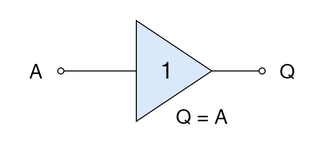
A Digital Buffer is shown in the following figure along with a Boolean expression.
Figure 1: Digital Buffer symbol
It is a unidirectional device and, as such, allows passage of input towards output i.e. from “A” to “Q”. From the Boolean expression, it is expressed that when input “A” is at logic “HIGH” or “1”, output “Q” is at logic “HIGH” or “1” and, similarly, when input “A” is at logic “LOW” or “0”, output “Q” is at logic “LOW” or “0”. The pattern shown is for a positive logic device such as the 74HC4050 CMOS Hex Buffer Gate.
A Buffer is used to isolate/ separate other devices or circuits from each other in order to prevent affection of functionality or impedance of each other. In addition, a Buffer is used as a driver of high current load, like a transistor, as its fan-out (output drive) capability is very high compared to its input signal. For example, the output port of a microcontroller is set to handle a maximum of 25mA and a buffer is a common solution to isolate sensitive microcontrollers from high-voltage output circuits and/ or to supply a high current. An open-collector Hex Buffer/ Driver can be used for this purpose such as TTL 74LS07 with a 30V output rating. In the following figure, a 74LS07 has been shown with internal circuitry.
Figure 2: TTL 74LS07 Hex Digital Buffer
Other Buffer Designs
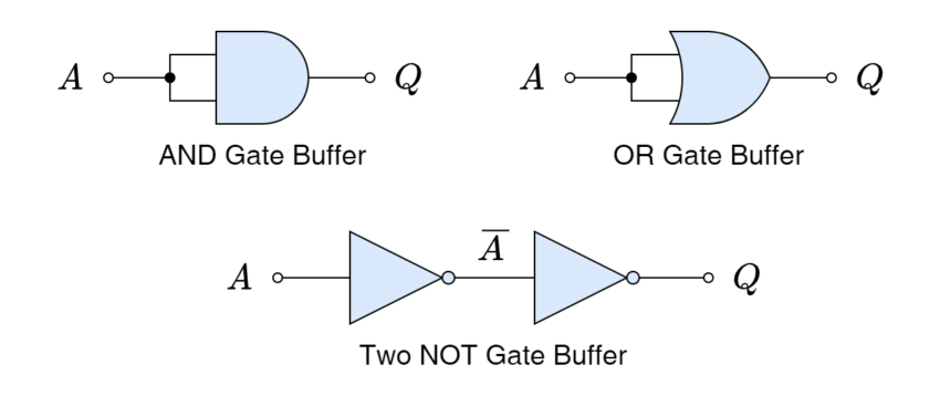
A digital non-inverting buffer can also be constructed using available Basic/ Standard logic gates such as OR, AND, or NOT gates. Simple combinations for accomplishing this non-inverting buffer are shown in the following figure.
Figure 3: Digital Buffer equivalent gates
Besides the above advantages of a Digital Buffer, there is a major limitation in its functionality as its output will always be connected to its input and that may affect output circuitry. Moreover, it limits flexibility in terms of control and reduction of circuitry. These issues can be solved by using a Tri-state buffer having three (03) different states at its output.
Tri-state Buffer
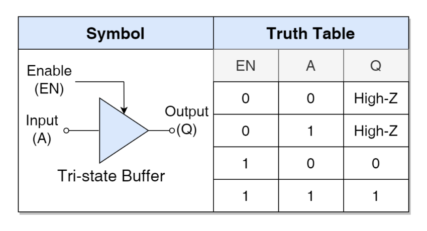
As the name says, it is a type of buffer having three (tri) states of output. These three states of the output of a Tri-state Buffer are achieved by different combinations of inputs and for this, Tri-state, an additional input is used compared to a conventional Digital Buffer. This additional input is a control input enabling the function of a buffer and is termed an “Enable” (EN) input. The usage of this additional input (EN) helps in achieving the third stage of High Impedance (High-Z) which isolates or open the circuit between input & output.
As such, a Tri-state Buffer has three states i.e. “OFF”, “ON”, and “High-Z”. The Control or Enable input can be active at logic “0” or logic “1” and the output of the Tri-state Buffer being non-inverting or inverting which all depends on the IC package. The most commonly used and available Tri-state Buffer ICs are TTL 74LC125 & 74LS126.
Tri-state Buffer Switch Equivalent
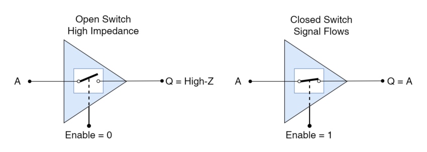
In the following diagram, equivalent circuits of Tri-state Buffer in switching modes are shown. The symbol of a Tri-state Buffer is similar to the conventional Digital Buffer but with an additional Control/ Enable (EN) input.
Figure 4: Tri-state Buffer switch analogy
When the “Enable” input is at logic “1” then buffer functionality is enabled and Tri-state Buffer will act as a conventional input. If the “A” input is at logic “0” then the “Q” output will be at “0” as well. Similarly, “Q” goes to logic “1” as “A” input goes to logic “1”.
Whereas, when the “Enable” input is set to logic “0” then the functionality of the buffer is turned off and the output is neither at logic “0” nor logic “1”. The output goes into a High Impedance (High-Z) state which represents an open-circuit condition and isolates/ separates input “A” and output “Q”. Anything present at “A” input is not reflected at “Q” output.
From above, it is observed that Tri-state Buffer has three states: logic “0”, logic “1”, and “High-Z” depending on the “A” and “Enable” inputs. Because of these three states, it is called a Tri-state Buffer. In the third “High-Z” state, it electronically isolates input “A” and output “Q”. Furthermore, at this state, the output is neither at logic “0” nor logic “1”. In a nutshell:
When “Enable” input is set to “0” or “LOW” state then Buffer’s output becomes open-circuited or goes into High Impedance (High-Z) state.
When “Enable” input is set to “1” or “High” state then Buffer passes the input signal directly towards the output.
The above functionality is based on a positively enabled (active-high) Tri-state Buffer and is reversed in case of negatively enabled or active-low enable input.
The above functionality of a positively enabled Tri-state Buffer can be represented in a Truth Table form, given below:
Figure 5: Tri-state Buffer symbol and truth table
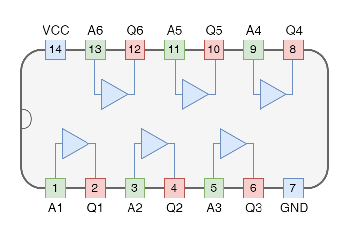
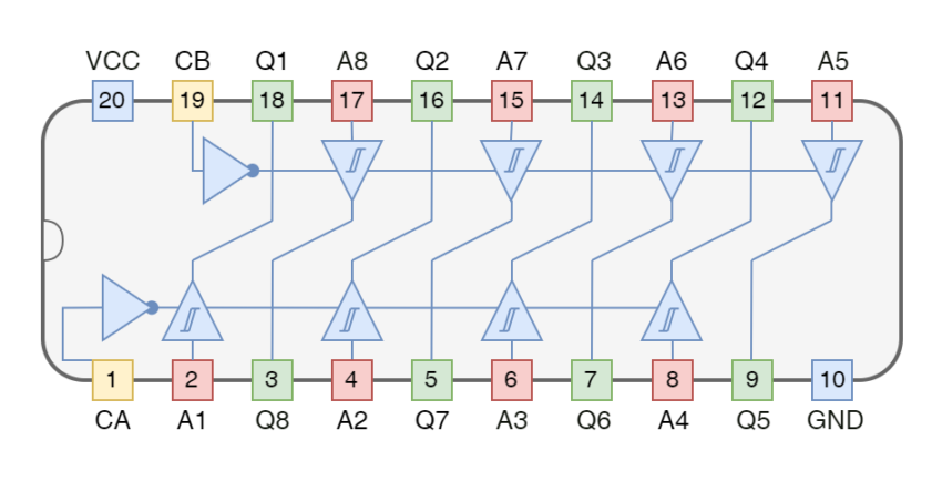
Commercially, Tri-state Buffers are available in IC packages having quad, hex, or octal Tri-state Buffers/ Drivers. In the following figure, TTL 74LS244 Octal Tri-state Buffer with internal circuitry is shown.
Figure 6: TTL 74LS244 Tri-state Octal Buffer
The above octal Tri-state Buffer/ Driver of 74LS244 is divided into two groups of four (04) buffers and each group has its own enable input. In the first group, inputs from A1 to A4 are controlled towards outputs from Q1 to Q4, respectively, using common enable pin “CA”. Whereas, enabling pin “CB” controls the remaining four Tri-state Buffers with inputs (A4 to A5) and outputs (Q5 to Q8).
Single Bus with Multiple Tri-state Buffers
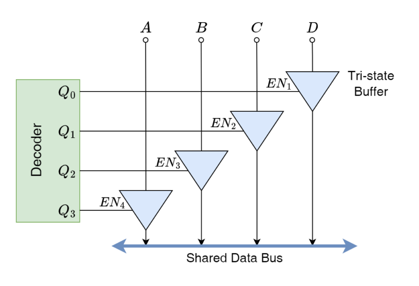
The third state (High-Z) of a Tri-state Buffer aids in connecting multiple devices to a single/ common bus. As this state of high impedance, isolates the input and output which helps in isolating undesired devices from the common bus by disabling relevant Tri-state Buffers and one of them is enabled, at a time, to transfer data towards the bus from the desired device. In the following figure, a decoder has been used to select one of the four devices, at a time, to connect with a common/ shared data or bus.
Figure 7: Tri-state Buffer controlled data bus communication
The devices are connected through Tri-state Buffers with a common/ shared data bus or wire, whereas, the control of each Tri-state Buffer is managed using a 2-bit decoder device. The use of a decoder helps in reducing the control wires from four (04) to two (02) only. Furthermore, by using a decoder, only one of the outputs will be set to “1” or “High” avoiding the interruption due to multiple devices communicating at the same time.
Using this decoder, one of the devices will be allowed to communicate with a shared/ common bus by setting the relevant Tri-state Buffer whilst other devices remain isolated due to their disabled Tri-state Buffers. This described combinational logic circuit resembles a 4-to-1 line multiplexer as the four data lines are passed to a single output using select lines. So, using a decoder and Tri-state Buffers, a multiplexer circuit can be constructed.
A Tri-state Buffer can be converted to a conventional Digital Buffer by connecting its “Enable” input to either “Vcc” or “Ground” depending on the type of Tri-state Buffer used. In this way, the Tri-state Buffer will be permanently enabled to pass any signal at input “A” toward output “Q” just like a conventional Digital Buffer.
Bi-directional Buffer Control
A Tri-state Buffer described above enables data to pass through from input “A” to output “Q” only but, not in the reverse direction. In order to enable data passage from both sides, just like a transceiver, two Tri‑state Buffers are placed in inverse parallel along with a NOT gate to invert one of the “Enable” inputs. In the following figure, a Bi-directional Buffer has been shown to demonstrate basic construction and to demonstrate working.
Figure 8: Bi-directional (transceiver) using Tri-state Buffers
The NOT gate at one of the “Enable” inputs of Tri-state Buffers, ensures that only of them remains enabled at a time. In this configuration, the “Enable” input is working as direction/ data flow control input. For example, when “Enable” is set to “HIGH” then data/ signal flows from “A” to “B” and, otherwise (in case “Enable” is set to “LOW”), from “B” to “A”. So, using “Enable” input, data/ signal can be set to flow in either direction allowing bi-directional communication. The Bi-directional buffers are also commercially available in IC packages such as TTL 74LS245 and CMOS 74ALS620 (inverting) and can be used as Bus Transceivers.
Bus Transceiver
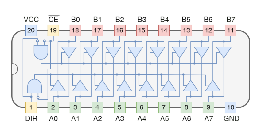
Bus Transceiver is a device based on Tri-state Buffers to allow data/ signal in bi-direction between two buses or to control bi-directional communication between two circuits. The Bus Transceiver is used in bus-oriented systems to facilitate controlled & bi-directional interface/ communication between data buses. In the following figure, an eight (8) line transceiver TTL 74LS245 has been shown.
Figure 9: TTL 74LS245 Octal transceiver
This octal Tri-state Buffer device can be used to interface to an 8-bit data bus for bi-directional & controlled asynchronous data communication. Using “DIR” input, the direction of data flow can be set. For example, when it is set to “HIGH” then data will flow from terminals labeled “A” to terminals labeled “B” and reverses the direction when “DIR” is set to “LOW”. In addition, Chip Enable “CE” input enables or disables the functionality of Tri-state Buffers. The bar on “CE” indicates that it is an inverted logic input and “CE” will be considered enabled when set to “LOW”.
Conclusion
A Transceiver is a device based on Tri-state Buffers which allows two-way (bi-directional) communication between buses or is used as an interface circuitry.
A Tri-state Buffer is a form of buffer that allows the passage of signal/ data without any alteration or decision-making.
A Tri-state Buffer has an additional input of “Enable” and features a third state of High Impedance (High-Z) compared to a conventional Buffer which has only two terminals and two output states.
A Tri-state Buffer has three (3) output states i.e. “HIGH”, “LOW”, or “High-Z” depending on the signal at data input and state of “Enable” input.
A Tri-state Buffer in a “Hi-Z” state behaves as an open circuit and isolates both terminals or input & output. This feature makes them suitable for communication with a single/ common/ shared data bus with multiple devices connected.
A bi-directional/ transceiver can be constructed by placing two Tri-state Buffers in an inverse parallel configuration and using a NOT gate at one of the “Enable” inputs. In this configuration, the “Enable” input acts as a directional control input.
A Bus Transceiver is based on bi-directional Tri-state Buffers which are used in bus-oriented systems or interface circuitry. An octal Tri-state bi-directional buffer, such as TTL 74LS245, can be used to interface an 8-bit device with a shared/ common data bus.
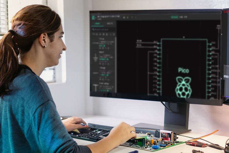
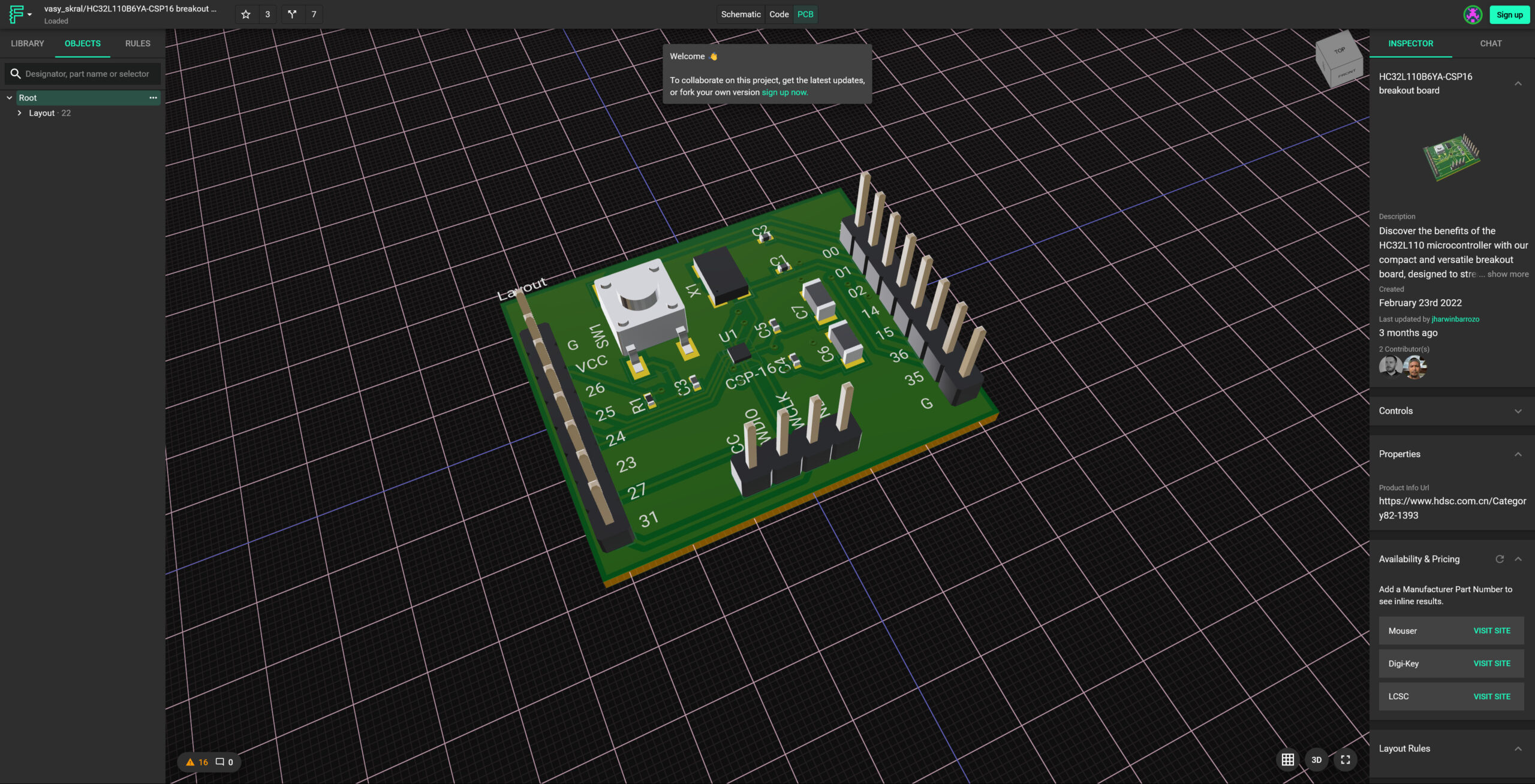
In today’s world of Generative AI and Large Language Models(LLM), it was only a matter of time before someone came up with the idea of incorporating generative AI into a PCB design tool. That is precisely what the team at flux.ai has accomplished. After securing $15M in seed funding, Flux.ai is making its platform available to the public. They have recently launched what they claim to be the “industry’s first AI-powered browser-based collaborative PCB design tool called Flux CoPilot. And in this review, we will learn about it.
What is Flux Copilot?
Copilot is a custom Large Language Model (LLM) developed by the team at flux.ai to understand the principles of electronic and circuit design.
Why do you need Flux?
If you are a PCB design engineer, you know how slow any hardware design and development process can be. Compared to the rapid development times that exist in the software industry.
One major challenge in the PCB design process is the lack of pre-established workflows at the designer’s disposal. So, when it comes to a new hardware design, it often involves tedious tasks like creating component footprints, laying out circuit blocks, routing traces, clearing ground planes, and calculating impedance. These tasks consume a significant amount of development time. Interestingly, no one goes through these tasks from scratch in software development. You wouldn’t write your encryption library or operating system, would you?
But that is what exactly hardware developers or PCB design engineers do! They build every single project from scratch every single time. This results in a significantly slow hardware design process. And we have yet to mention the additional time it takes for PCB manufacturing and assembly.
What is FLUX.AI?
It was to address all these challenges that Flux was born. Flux is a browser-based electronics design tool with built-in support for modern hardware design methodologies: reusability, collaboration, and simulation.
It’s a browser-based tool, so you don’t need to download anything to your computer. Just head over to flux.ai and create an account. When that is done, you are ready to go. If you are accustomed to google workspace (docs, sheet, keep, slide), you will notice that the UI is very similar; the share button and the user icon are in the same place as in Google. You’ll also find the interface familiar if you’re used to using EDA software like Eagle, Altium, and KiCad. Additionally, navigating through the UI with the default dark theme makes it easy on the eyes.
Getting started with Flux
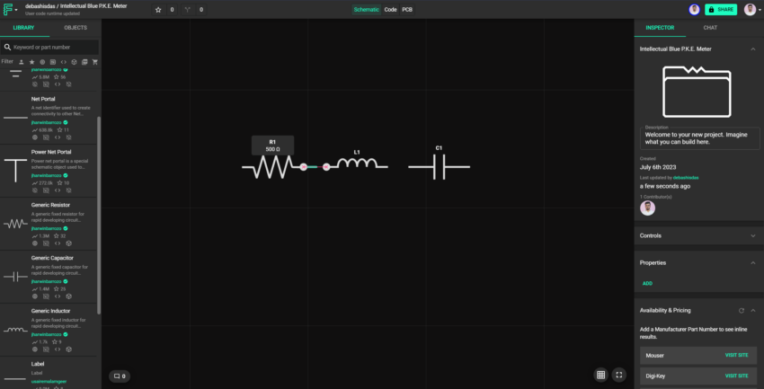
Once the sign-in process was complete, we created a new project. You will get Five Private Projects and Unlimited Public Projects on a free account. We started by creating a basic RLC series circuit in the editor. While working, the performance was fast, and dragging elements from the sidebar to the editor was a joy.
The wiring process was also very easy; to wire up one component to another, you need to click on the terminals of a component, and the wire will appear.
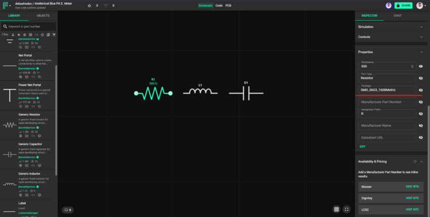
Changing a component’s properties is also very easy. If you want to use a through-hole component instead of an SMD one, select the component, and scroll down to the properties tab. You can find the package information there, click on that, and change the device’s package.
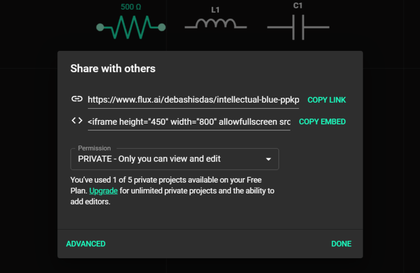
Real-time collaboration is supported, which is a big game changer for the electronics industry. No more file juggling with Dropbox or Git commits! However, we need the snap-on-grid feature, which is a big letdown for us as we use it in almost every design. That is why components can appear to have slight misalignment, and it causes confusion in wire connections.
We have also encountered additional bugs while working; dragging and connecting wires can be unintuitive, and you will need some practice before you get the hang of it. Additionally, when trying to drag an element on top of a wire, it doesn’t work as expected. Instead of replacing the wire with the component, it causes a short circuit.
However, most of these issues are minor and can be looked away. Currently, the focus is primarily on adding exciting new features rather than prioritizing resolving these minor bugs. And speaking of new features…
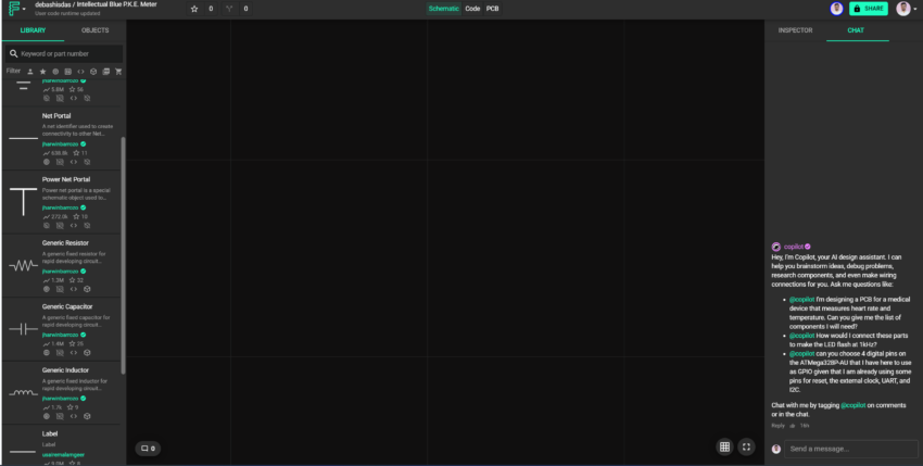
We tried the AI Copilot: An AI Assistant with Expertise in Electrical Engineering
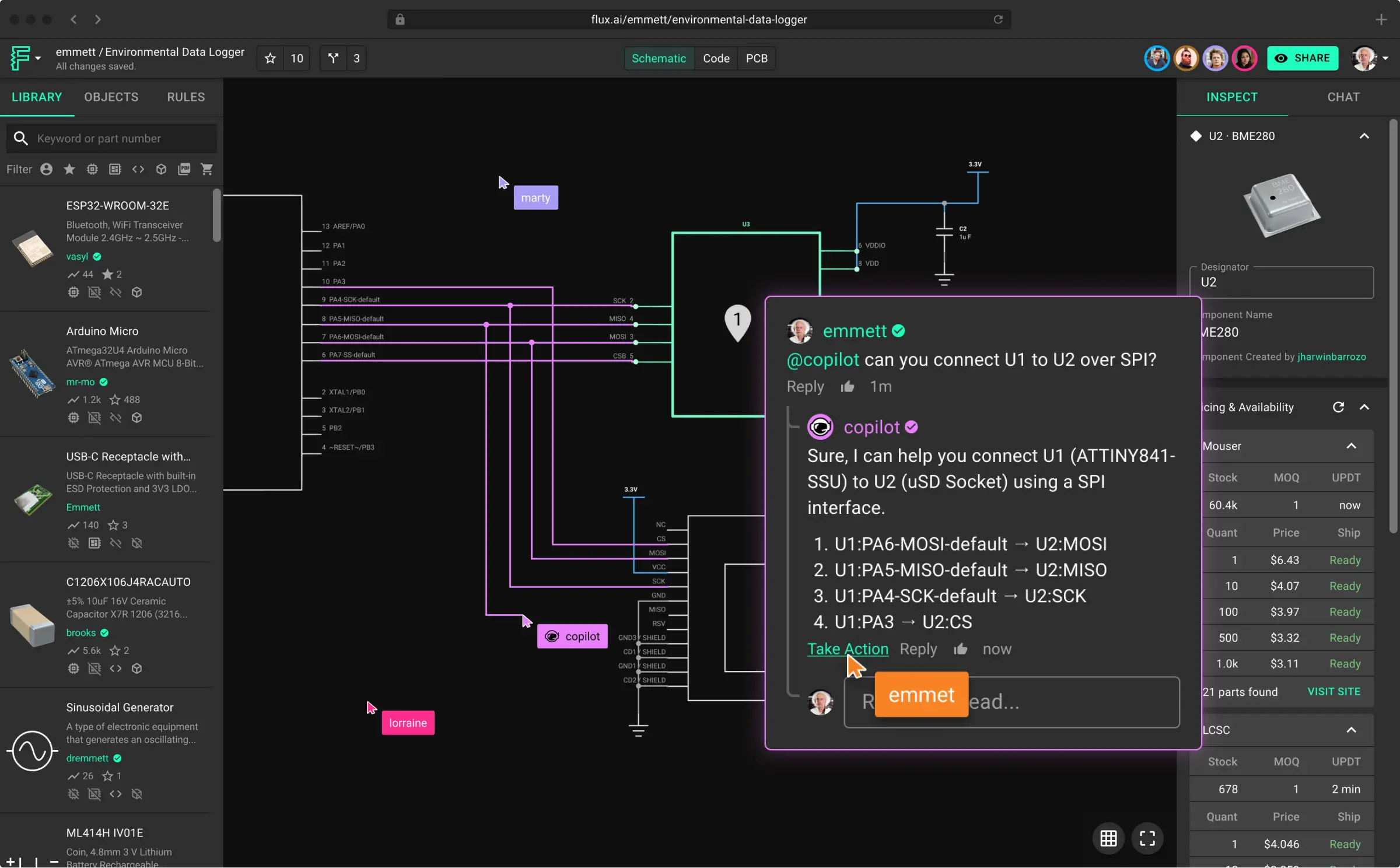
Flux Copilot is a specially trained large language model (LLM) that you can find on the right-hand side of your screen referred to as chat. With its deep electronic and electrical knowledge, it can do various tasks.
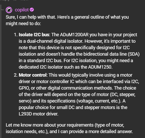
It is chatGPT for electronic projects but with a full understanding of electronic and electrical design. So we started with an actual practical problem and asked @copilot if I wanted to isolate the i2C of this microcontroller and drive some motors.
We didn’t say anything about the rest of our circuit, and we were very surprised at how good the response was,
Not only did it give us the part numbers, but it also taught us how to connect the i2c isolator to the microcontroller. What’s even more impressive is that it automatically detected the microcontroller from the editor window without us having to specify it. This level of automation was truly remarkable, to say the least.
Check out the reference documentation if you want to know more about AI Copilot.
PCB viewer/editor
If you have prior experience using Eagle PCB design software, you will find the interface of Flux will look very familiar to you. just like Eagle, Flux automatically transfers all the parts from the schematic to the PCB view, provided there are no errors. This makes it incredibly easy to experiment with different footprints and layouts without pulling changes from your schematic to PCB every time you make a change.
However, it could have been a more redefining experience because the interface lagged a bit and used a ton of resources while operating. If you are used to Eagle and Altium, it comes with default DRC settings, but for Flux, you need to set your DRC before you start your design.
You will find the code tab lying dormant between the board and schematic; we assumed it was something like Eagles ULPs, which we are familiar with, but it can do much more than any ULP or custom script can do. You can automate partsvalue and package assignments, you can assign the part type, generate a custom simulation model and do more cool things.
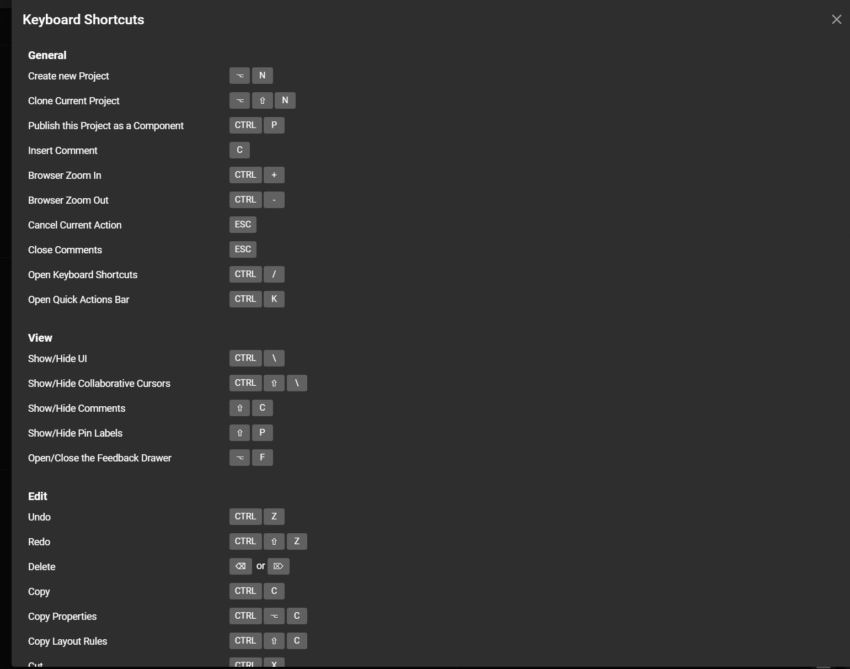
Keyboard shortcuts and circuit simulation
Like other EDA tools, Flux also comes packed with handy keyboard shortcuts. The most interesting part is that there is a custom assignment function in Flux with that you can assign your favorite components to the number keys 1-5 for quick access. But here’s the catch: we quickly ran into a problem because we started running out of component slots in no time.
You can access the keyboard shortcut list in Flux by pressing the Ctrl+/ key, just like you did for Google Workspace. So we spent some time experimenting to see how fast we could make our workflow.
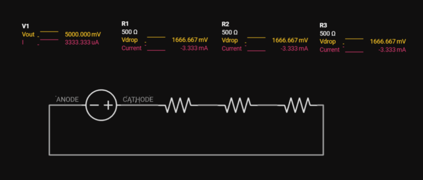
Flux has an integrated simulator, but you will not find any dedicated “Simulation” tab in the tool because it runs automatically by default.
The only requirement you need to care about is the part should have a simulation model assigned to it. That means you cannot simulate more complex parts like microcontrollers, and you are limited to simple parts like transistors, resistors, capacitorinductors, and basic ICs. If you are savvy enough, you can write your simulation model using the Fulx system’s code editor.
Conclusion
I was very excited to try out Flux because it’s one of those tools which can change the aspect of electronic and hardware design forever. Yeah, there are already some pretty advanced EDA tools out there, but here’s what we’re thinking: in the future, Flux can do way more than just suggest changes for the schematic. Imagine this: Copilot, could dig up cheaper alternatives for parts and automatically swap them out in the schematic. It can even help you tweak your PCB design. Say you wanna replace a small capacitor with a bigger one that has a different footprint. that will definitely mess up your PCB connections. No worries! Copilot can handle those kinds of design tasks without breaking a sweat. Trust me, Flux is the game-changer we’ve been waiting for in electronic and hardware design!
Purchasing Information
Flux.AI has a community-first approach with its pricing model. The free version of this tool provides almost all functionality for all users indefinitely.
For companies, both small and large, the ‘Pro‘ or ‘Organization‘ options are available at $15/month and $45/month respectively. These offer private projects and additional business-oriented features.
If you want to check the pricing information yourself, you can check out the attached link.
Qualcomm Technologies has launched the 212S Modem and the Qualcomm 9205S Modem chipsets with satellite capability for remote monitoring and asset tracking for Internet of Things (IoT) devices. These modems are developed in collaboration with Skylo to offer low-power and advanced wireless connectivity for IoT devices, allowing them to connect to both satellite and cellular networks. This dual connectivity ensures that devices can stay connected even in remote areas with limited terrestrial network coverage.
Both these chipsets integrate with the Qualcomm Aware Platform, which offers NTN connectivity services and device management in remote areas. This integration enables efficient monitoring and management of devices operating in remote locations, facilitating critical decision-making processes that depend on accurate and real-time data. The Qualcomm Aware Platform improves IoT deployments’ effectiveness, providing businesses with valuable insights for improved operational efficiency and productivity.
“Our Qualcomm 212S and Qualcomm 9205S chips take our IoT tracking and monitoring capabilities one step further, providing connectivity and coverage even in the most remote areas. These products also further showcase our ability to bring and scale superior innovations to even the most challenging and complex IoT environments.”
The Qualcomm 212S Modem is designed for stationary IoT devices that require satellite communication for advanced connectivity in off-grid locations. The modem is ideal for various applications, such as collecting telemetry and data from water and gas tanks, meters, and other infrastructure equipment. It can also be used for utility grid monitoring, early fire detection reporting, on-shore and off-shore mining installations, and environmental management.
The Qualcomm 9205S Modem incorporates Global Navigation Satellite System (GNSS) capabilities, enabling accurate location tracking for IoT applications. It comes with a similar architecture to the Qualcomm 9205 Modem. The modem also supports hub-type use cases through its robust application processor and peripheral support, enabling a wide range of IoT applications to benefit from its capabilities.
“We will deliver satellite connectivity through the Qualcomm Aware Platform using our network of satellite operators to power a range of IoT use cases with optimized integrations through the Qualcomm 212S and 9205S modems for stationary and in-transit uses.”
The Qualcomm 212S Modem will be available later this year, while the Qualcomm 9205S Modem is already available.
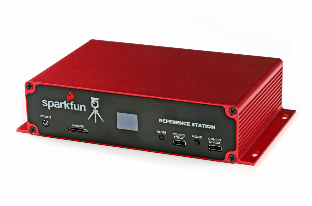
SparkFun introduces RTK Reference Station, a hardware device for high-precision geolocation, surveying, and time reference. The platform leverages Real Time Kinematics (RTK) to deliver improved positional accuracy. It combines signals from Global Navigation Satellite Systems (GNSS) with a collection data stream to elevate the accuracy of satellite positioning receivers.
SparkFun started the RTK series of products that offer GNSS receivers with out-of-the-box options that can be used without configuration. The product line includes RTK Facet L-Bank, which has the ability to achieve centimeter-grade measurements, and RTK Express Plus, designed for post-processing for autonomous vehicles and logging.
SparkFun RTK receivers can achieve high accuracy by utilizing Real Time Kinematics (RTK) technology. In addition to the normal signals received from Global Navigation Satellite Systems (GNSS), the RTK receiver also takes in a Real-Time Correction Message (RTCM) data stream. By incorporating this correction data, the receiver can calculate its location with an accuracy of 1cm.
The SparkFun Reference Station is built upon the ESP32-WROOM processor and the U-Blox ZED-F9P multi-band GNSS module. It uses the same open-source firmware as other SparkFun RTK products, ensuring compatibility across the product line. The Reference Station offers 10/100 Mbps Ethernet connectivity, allowing for fast and reliable data transfer. It can also be powered by Power-over-Ethernet (PoE), providing a convenient power supply solution.
The U-Blox ZED-F9P GNSS module is used for high-precision geolocation, which is connected via a high-speed SPI interface, enabling a significant increase in the transfer speed of GNSS data. This improvement empowers users to log RAWX and SFRBX data from all constellations at a high frequency of 20Hz, providing unparalleled data collection capabilities.
SparkFun Reference Station offers a solution for those with a Network Time Protocol (NTP) time server for their Ethernet network. By deploying the Reference Station as an NTP server, you can improve the accuracy of timekeeping across your Ethernet network.
The Reference Station comes with built-in support for DHCP (Dynamic Host Configuration Protocol), which simplifies the setup process by automatically assigning an IP address to the device. However, if you prefer a fixed IP address for your NTP server, the Reference Station allows you to configure it accordingly.
The RTK Reference Station is available for purchase on the official SparkFun website, priced at $699.95 USD. Interested people can visit the hookup guide for more information.
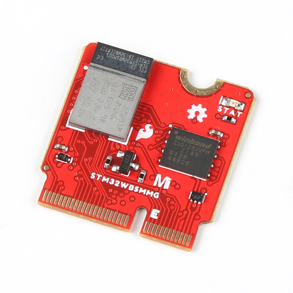
SparkFun Electronics has expanded its MicroMod ST product line by introducing the SparkFun MicroMod STM32WB5MMG Processor. The processor board combines computing capabilities with wireless functionality, all packed into a single M.2-connectable module.
As the name suggests, the MicroMod STM32WB5MMG Processor is built around the STMicroelectronics STM32 processor core, which is a low-power module, an ideal choice for battery-powered applications. It features a combination of two Arm Cortex processors: a Cortex-M4 processor with FPU and ART for primary computing tasks and a Cortex-M0 processor dedicated to running the 2.4 GHz RF stack.
The STM32WB5MMG processor supports various wireless protocols such as 2.4 GHz wireless communication and compatibility with Bluetooth Low Energy 5.3, Zigbee 3.0, OpenThread, and 802.15.4 proprietary protocols. This wide communication protocol makes it a good choice for a wide range of applications that require reliable and efficient wireless connectivity.
The Cortex-M4 CPU operates at a frequency of up to 64 MHz, ensuring efficient processing of data. Including a floating-point unit (FPU) single precision improves the module’s capabilities. The FPU supports all ARM single-precision data-processing instructions and data types. Additionally, the processor implements a memory protection unit (MPU), which enhances the security of applications by isolating memory regions.
In 2020, following the introduction of the SparkFun Qwiic connect system, SparkFun unveiled a new modular interface that utilizes the M.2 standard– MicroMod. This interface allows for connecting a microcontroller processor board to different carrier boards. By leveraging the convenience of solderless interfacing, developers can select their preferred processor board and easily connect it to standalone carrier boards.
SparkFun has previously launched a MicroMod STM32F405 processor board with its Arm Cortex-M4 32-bit RISC core. For situations where there is limited workspace but a need for enhanced power, this compact processor board offers a cost-effective and user-friendly development platform.
The SparkFun MicroMod STM32WB5MMG Processor is priced at $19.95 USD. Interested people can check out the official product page for more details.
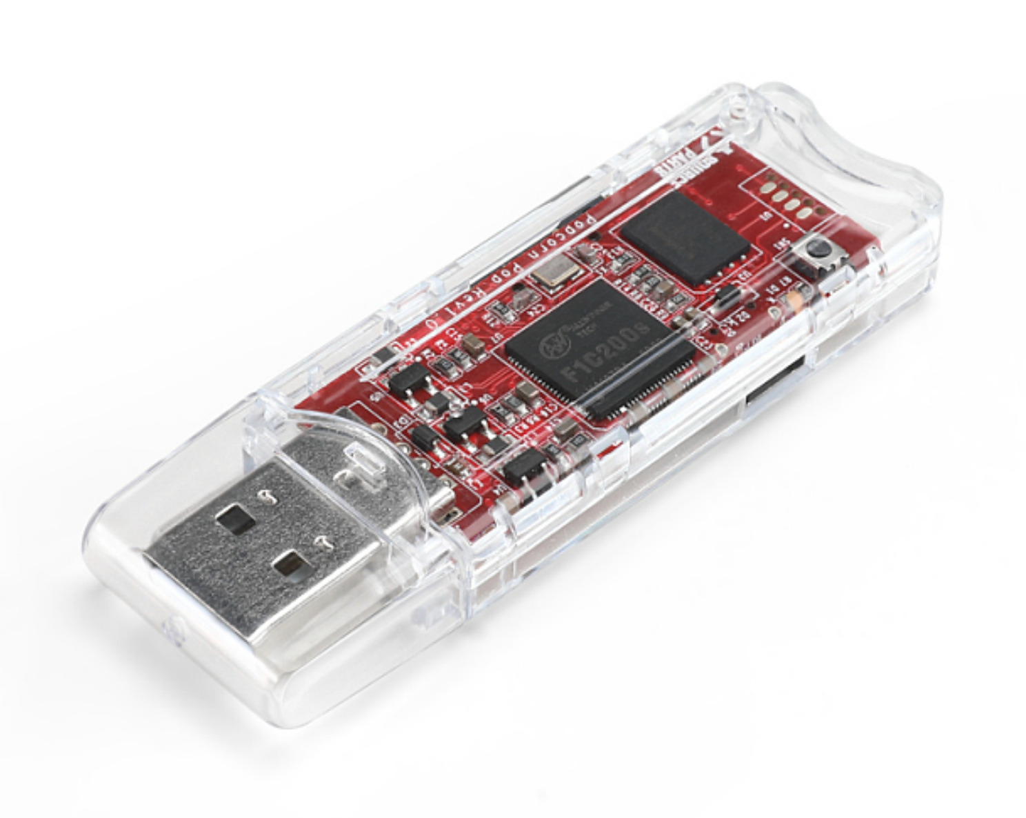
Source Parts has launched a USB computer called the Popcorn Computer PopStick. This compact-sized device is designed to provide a computing experience by plugging directly into any computer with a USB-A port or any other USB port with the help of a simple adapter.
Furthermore, the PopStick can also be connected to various cell phones or devices through USB Micro-B, USB-C, or Lightning connectors when used with an appropriate adapter. Once connected to a host device, the PopStick can appear as any desired USB device, offering greater possibilities for customization.
The Popcorn Computer PopStick is built around the Allwinner F1C200s SoC featuring the ARM9 CPU architecture. It supports full HD video playback, including popular codecs such as H.264, H.263, and MPEG1/2/4, making it ideal for multimedia applications. Users can leverage high-quality audio with an integrated audio codec and I2S/PCM interface.
Specifications of PopStick USB computer:
SoC: Allwinner F1C200S SoC featuring ARM926EJ-S (ARMv5TE) at 533 MHz clock frequency
Memory: 64 MB embedded DDR1
Storage: 128 MB SPI NAND flash for operating system and MicroSD card slot
Interfaces: 1x USB-A connector for connecting to a host computer and 1x USB Micro-B connector to present a dedicated USB-to-Serial console for direct control
The PopStick USB computer comes with out-of-the-box software support. It is shipped in a preloaded simple Linux environment that automatically sets up a Gadget USB Ethernet and USB Serial device during booting. This allows users to easily SSH into the device, similar to any other Linux computer. Simultaneous connection to a Serial Console is also supported.
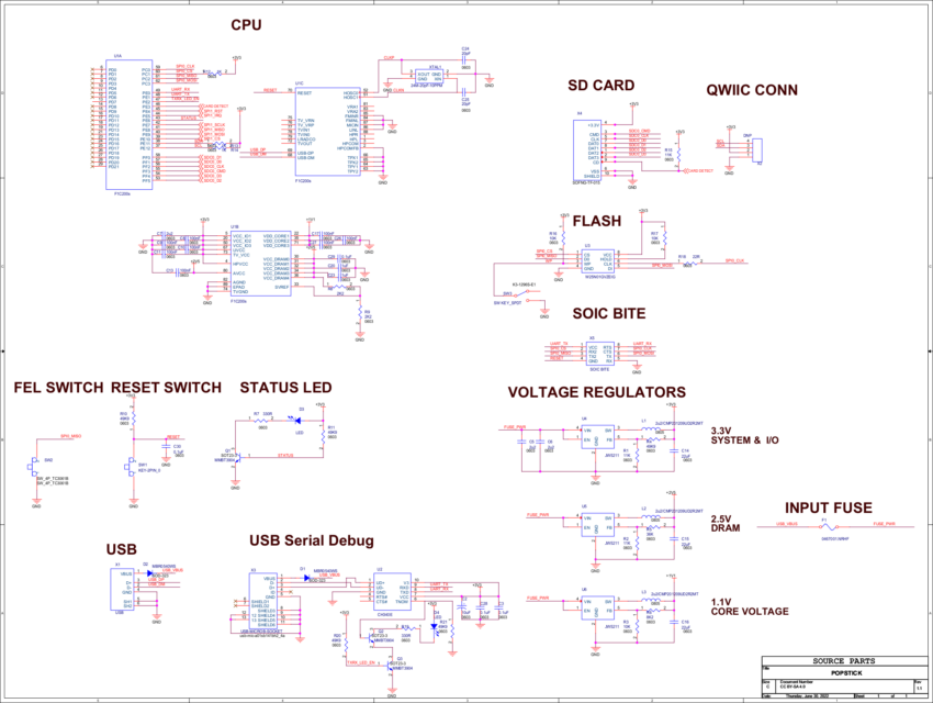
The company has made the design files available for public use. The official GitHub repository has schematics and design files for engineers who aim to develop a next-gen hardware platform based on the currently open design.
Popcorn Computer PopStick is available in multiple configurations. The 32GB MicroSD card version, priced at $37.99 USD, offers enough storage for applications and data. For budget-conscious users, the basic option, priced at $29.00 USD, excludes flash storage.