Reverse-engineering the ALU of 8008 microprocessor

Ken Shirriff has written an article on reverse engineering the ALU of the 8008 microprocessor:

A computer’s arithmetic-logic unit (ALU) is the heart of the processor, performing arithmetic and logic operations on data. If you’ve studied digital logic, you’ve probably learned how to combine simple binary adder circuits to build an ALU. However, the 8008’s ALU uses clever logic circuits that can perform multiple operations efficiently. And unlike most 1970’s microprocessors, the 8008 uses a complex carry-lookahead circuit to increase its performance.
The 8008 was Intel’s first 8-bit microprocessor, introduced 45 years ago.1 While primitive by today’s standards, the 8008 is historically important because it essentially started the microprocessor revolution and is the ancestor of the x86 processor family that are probably using right now.2 I recently took some die photos of the 8008, which I described earlier. In this article, I reverse-engineer the 8008’s ALU circuits from these die photos and explain how the ALU functions.

Reverse-engineering the ALU of 8008 microprocessor – [Link]

Low-Cost FPGA With Reconfigurable Electronics Feature

Iolinker is a cheap 64 FPGA board with a MachXO FPGA that functions as a dynamically configurable IO matrix. Its main functionality, besides IO extension, is to dynamically set up a matrix of GPIO connections, that allow direct pass-through of high-frequency signals. Circuits can thereby be configured and programmed on the fly. There are UART / SPI / I2C connections that allow for easy integration of up to 127 chips connected in parallel.

Thanks to the open source library, Iolinker allows developers to create reconfigurable, easy to self test electronics within minutes. It can be used to be an IO extender and can output PWM signals. In addition, its revolutionary “IO linking” feature allows to dynamically pass through high-speed signals between IOs, better than any microprocessor ever could.

Check this teaser about the new board:

Iolinker has the following specifications:

  • Reprogrammable FPGA board with Lattice LCMXO3L-4300E-5UWG81CTR50
  • Preprogrammed and usable out of the box as your IO interface of choice.
  • 49 GPIOs for PWM or IO extension usage, VCCIO is 3.3V.
  • Boards can be connected in parallel, to create endless IO extension.
  • IOs can be linked to each other, i.e. you tell the FPGA to connect them, and it forwards the input signal from one pin to another. (Read more about the iolinker chip function.)
  • UART, SPI or I2C interfaces are available.

In order to make the ultimate IO interface for users, the team are accepting feature requests at the contact page.

In short, the Iolinker board is easy to use and can reconfigure schematics on the fly, what makes it ideal to reduce prototyping time and jumper cable mess, and to maximize the ability of using IO extensions.

More technical details about Iolinker and its price will be announced soon at the Kickstarter campaign at Feb 14. Some special offers are for everyone who register in the website’s newsletter, so register now and stay tuned!


Introduction to Digispark

runtimeprojects.com has a quick review of the Digispark board. It’s a really interesting mini board that can be used in small projects using Arduino IDE.

In today’s blog post we’ll analyze one of the smallest and most practical boards out there. The Digispark board. It’s size, including the USB port, is 25mm x 18mm (so tiny)!! This little board is powered by an ATTINY85 chip and clocked to 16.5Mhz. For conveniece, it has a built in USB port and can be plugged into a your computer without cables or adapters. Now that’s pretty awesome! It is powered by either the USB port, from the +5v pin with regulated 5v or from VIN pin if unregulated. The VIN pin supports from 7v to 35v although less than 12v is recommended by the manufecturer.

Introduction to Digispark – [Link]

NTP synchronized clock

The Network Time Protocol (NTP) is the most commonly used internet time protocol for synchronizing locally running clocks to a more accurate reference clock server. In United States, the official time is provided by the National Institute of Standards and Technology (NIST). The NIST servers listen to a NTP request, and respond by sending a 64-bit UDP/IP data packet containing the time in UTC seconds since January 1, 1900, with a very high time resolution of 200 picoseconds. Raj from Embedded Lab illustrates in his new tutorial how to make an ESP8266 based internet clock that is synchronized with the NIST time server for accurate timekeeping. An ILI9341-driven colorful TFT LCD is used to display time in both analog clock dial and digital formats. Raj used EasyESP-1 board for this tutorial and developed the firmware for his internet clock using Arduino IDE.

ESP8266-based internet clock

Export Eagle Libraries With SnapEDA

Although the new Eagle subscription model by Autodesk will bring much-needed features to the software, many users after the announcement had decided to move their work to other alternatives, such as KiCad, Altium, Cadence, etc.

One of the challenges was to convert the libraries made by Eagle to be compatible with other software programs. SnapEDA solved that by offering a new free tool that translates Eagle libraries to KiCad, Altium, OrCad and other formats.

SnapEDA is a parts library for circuit board design provides free symbols, footprints, and 3D models for millions of electronic components. The goal behind SnapEDA is to build one trusted, canonical source of electronics design content that everyone can benefit from.

To convert your Eagle library just upload your file here, then you can re-download it in any format through your uploaded models page. The video below demonstrates the converting process:

Currently, all the uploaded parts will be public on SnapEDA until the private version is released. All parts are clearly marked as user-generated content and attributed to the uploader, and can be deleted at any time.

“We are big fans of Eagle and the new changes they’re making, and are confident that the subscription model will bring much-needed features to the software. But we also understand that it is (for many) a showstopper. Hopefully this free tool is helpful to those for whom this is the case.” – SnapEDA

Try now this tool and convert your files here!

Increasing Battery Life With UB20M Voltage Detector

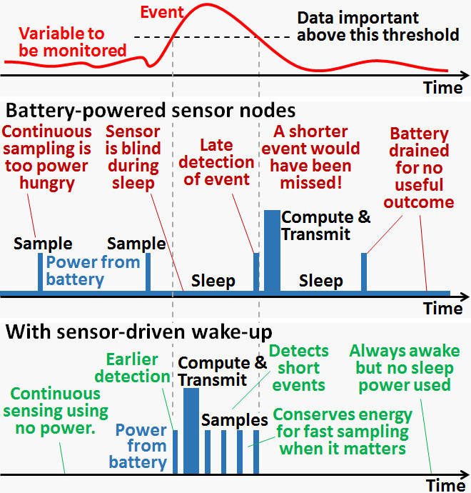
Engineers at the University of Bristol have developed a three terminal pico-power chip that can cut standby drain in sensor nodes – even compared with today’s low-power microcontrollers.

It does this by replacing the low duty-cycle sleep-wake-sleep pattern used on MCU-based sensor monitors, with ‘off’. A voltage detector powered by the sensor – there is no other power source –  starts the processor when the sensor produces a voltage.

At 5pA (20°C 1V), power draw from the sensor through the input/supply pin is so low that the chip can directly interface with high-impedance sensors such as antennas, piezo-electric accelerometers, or photodiodes. With so little current required, the chip does not collapse the sensor voltage.

“It will work from five infra-red diodes in series, powered from a TV remote control 5m away, or an un-powered accelerometer”, Bristol engineer Bernard Stark told Electronics Weekly.

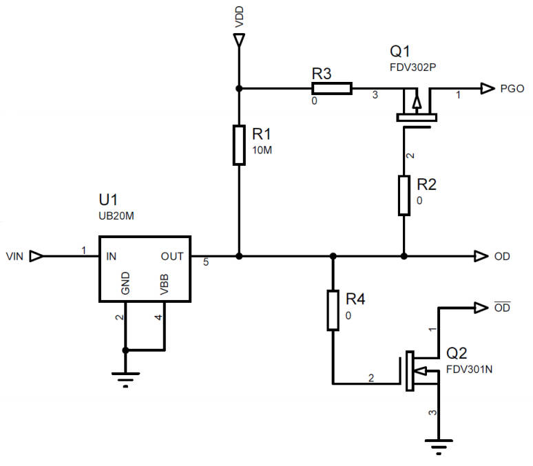
Called UB20M, the only power it draws from the system is 100pA(max) leakage through its open drain output transistor. Input threshold is set at 0.6V.

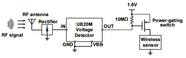
Once the sensor presents greater than 0.6V to the input, the output FET turns on (RDSon~800Ω), and its low resistance can either be used to turn on a p-FET to power up a microcontroller, or can wake a microcontroller from sleep.

In an extreme application example, said the University, an earthquake detector could be held in sleep for years, until a tremor caused the chip to wake its host.

Despite its impedance and sensitivity, the device can withstand 20V on its input/supply pin, and it has ESD protection. Maximum output pin parameters are 5.5V 7mA. Output turn-on time is 0.25μs, while turn-off depends on load resistance and capacitance – typically 8μs with a 5MΩ load and 180μs with 100MΩ.

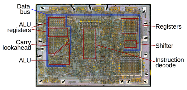
Because patents are pending, exactly how the chip works is not being disclosed. It has around 40 transistors, and is made on a 180nm CMOS process, is all Stark could say.

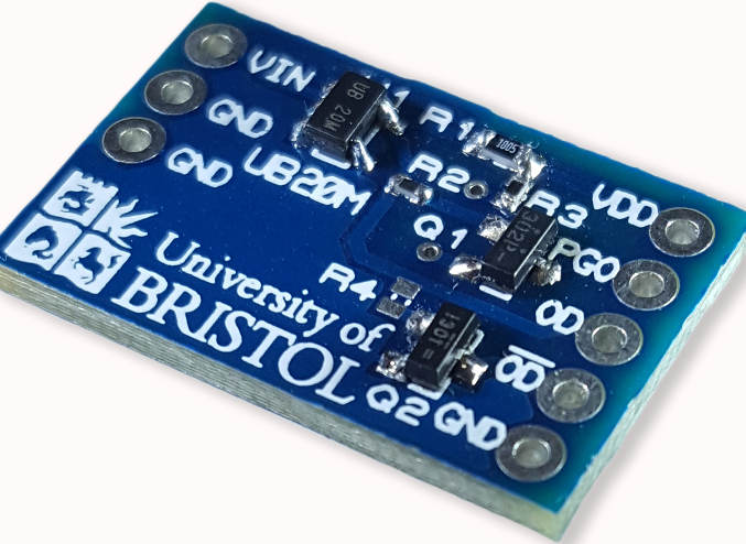
Samples are available – through a multi-project wafer deal with Europractice and IMEC, fabricated at AMS in Austria, and the University has created an evaluation board. Due to Europractice and IMEC going the extra mile, said Stark, samples are in SOT323-5 rather than clunky research packages.

The team cautions that anyone trying the chip will need to understand high-impedance circuits, as otherwise stray mains fields, for example, will trigger it continuously and the output transistor will remain on. Lengthy sensor connections should be avoided.

In general, the sensor has to be connected to the input/supply pin with enough parallel resistance to leak away stray charge and ensure the UB20M turns off.

“We are now working on ways of bringing other power drains such as data-capture, computation, and transmission, to within the nW-power budget of a sensor, completely eliminating batteries from sensor nodes,” said the University. “An example of this (right) is where power management with a few tens of nW quiescent is actively matching its input impedance to an 80MΩ energy harvester with 10 ms intermittent output pulses.”

UB20M data sheet and eval board details can be reached from this introductory web page, and there is an introductory video.

Source: Electronics Weekly

12V @ 120mA Transformerless Power Supply

The circuit provided here is a transformer-less non-isolated power supply which is capable of delivering an output of 12V at 120mA current for an input voltage varying from 85VAC-265VAC. The LNK304 is the heart of this circuit which supports buck boost and flyback topologies. This project is low in cost and simple when compared other tramsformer-less power supplies.

Features:

  • Input(V): 85V AC to 265V AC
  • Output(V): 12V DC
  • Output load: 120mA
  • PCB:75mm X 35mm

12V @ 120mA Transformerless Power Supply – [Link]

TI claims first for zero-drift, zero-crossover op amp: precision & linearity

by Graham Prophet @ edn-europe.com:

With precision and high input linearity in a single high-performance device, Texas Instruments says it has the first operational amplifier (op amp) to offer both zero-drift and zero-crossover technology. The OPA388 op amp maintains high precision across the entire input range for a variety of industrial applications, including test and measurement, medical and safety equipment, and high-resolution data-acquisition systems.

TI claims first for zero-drift, zero-crossover op amp: precision & linearity – [Link]

XPlotter, The All-In-One Plotter, Engraver and Laser Cutter

XPlotter is an affordable and easy to use desktop plotter, Laser cutter and engraver. It is designed to create a new definition of plotter. By integrating the laser engraver and cutter into the mechanism, it becomes a versatile desktop tool for artists, craftsmen and makers to set their imagination free.

The all-in-one machine can simulate real effects of handmade drawing and writing, can cut out and laser engrave on different materials. In addition, it has the capability to pick and place objects perfectly!

This machine is now live on Kickstarter, check out the video campaign to see XPlotter in action:


The writing of XPlotter is outstandingly similar to the real hand writing thanks to the angle of writing and the programmed process. Now you can do your paperwork or write your homework as neat as possible. Also you have the option to choose from a variety of fonts and pens! Drawing outputs also look so real because of demonstrating shadows and tiny tiny details.

A wide range of materials like paper, leather, fabric, cloth, and cardboard are able to be engraved by the laser engraver feature of XPlotter. Short time is needed to engrave your artworks due to the powerful laser equipped with the machine. Safety goggles are included too for making sure that users cope with laser safely.

This personal robot that is dedicated to write, draw and engrave for you has no limits. XPlotter team made a built-in vacuum pump system to enable XPlotter to pick and place at a high speed and features a precision within 0.012mm. It only takes you a few minutes to change the end effector into a vacuum suction cup, which is powerful enough to grab spherical items.

Amazingly, the team behind XPlotter has open-sourced the operation interface to welcome more applications made by users through the secondary development.

In short, these are the specifications of this amazing tool!

Check out this comparison between XPlotter and its alternatives.

The retail price will be around $500 but now you have the chance to get the basic XPlotter via the crowdfunding campaign for only $349. The full kit including engraving and pick and place is priced $529, where the final retail after Kickstarter will be $629. This campaign still has 52 days to go, you can check the campaign page now and choose your reward.

More videos of XPlotter in action can be found at this Youtube profile and the official website.

Teardown of a Peaktech 6225A

Teardown and analysis of a Peaktech 6225A power supply from ElectroBob:

I got a Peaktech 6225A power supply to power some things, as it seemed like a good deal, going beyond what one might find normally in these types of supplies: more display resolution and supposedly, lower noise. For this price, this supply is a good deal compared to other similar ones on the market. Let’s see how it performs.

Teardown of a Peaktech 6225A – [Link]

TOP PCB Companies