
In this instructable I am going to show you how to build a weather station that logs the information that it collects on a sd card.
DIY Data logging weather station under $15 – [Link]
In this instructable I am going to show you how to build a weather station that logs the information that it collects on a sd card.
DIY Data logging weather station under $15 – [Link]
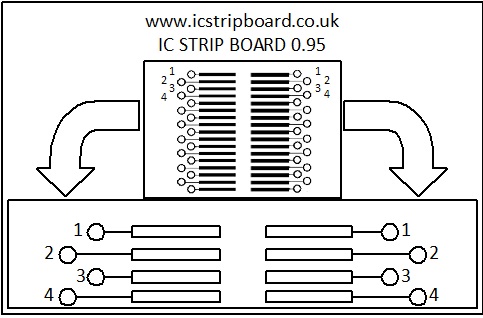
ICStripBoard is a innovative cheap tool to enable rapid prototyping of surface mount integrated circuits (IC’s) and allow their usage in prototype electronics projects.
Inline surface mount IC’s come in a Variety of packages which are different sizes and these Printed Circuit Boards (PCB’s) have been designed to accommodate the majority of IC’s. Available in the four standard IC pitches (space between IC pins) of 0.5mm, 0.65mm, 0.95mm and 1.27mm. These boards have been designed as long strips on thin (half the standard thickness) 0.8mm FR4 boards which can easily be cut to the correct amount of pins which the IC in question has. This allows the strip to be cut for multiple IC’s on multiple projects.
The cut pieces can easily be soldered and glued to other prototyping products and in conjunction with traditional through hole components can be used to create unique electronic prototypes. These boards will allow you to experiment with multiple IC’s without having to build PCB’s and is far cheaper than buying alternative break out boards due to the fact you cut them to size and the pattern repeats down the strip allowing this to be done multiple times. Continue reading “ICStripBoard – PCB rapid prototyping tool”
@ blog.tindie.com
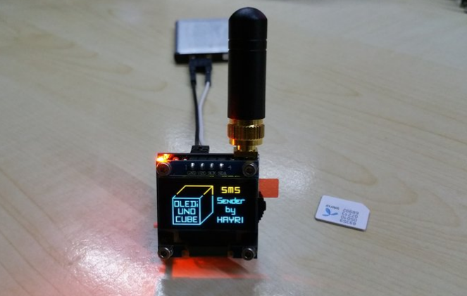
This quad band GSM board is claimed to be the worlds smallest of its kind. We have no way to verify this bold claim but let’s all agree that this is a pretty small board that lets you send texts and make calls. The GSM feature is an addition to the OLEDiUNO Cube range that we have mentioned previously on the blog.
Send Texts or Make Calls With This Tiny GSM Board – [Link]
Researchers have demonstrated the high-performance potential of an experimental transistor made of a semiconductor called beta gallium oxide, which could bring new ultra-efficient switches for applications such as the power grid, military ships and aircraft.
The semiconductor is promising for next-generation “power electronics,” or devices needed to control the flow of electrical energy in circuits. Such a technology could help to reduce global energy use and greenhouse gas emissions by replacing less efficient and bulky power electronics switches now in use.
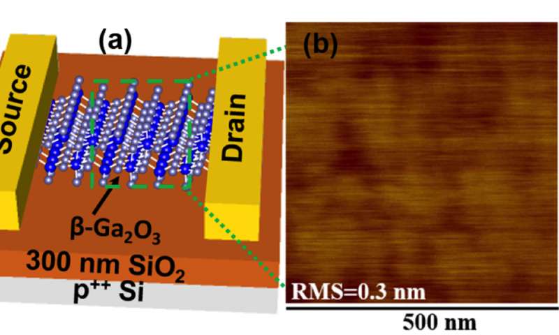
The schematic at left shows the design for an experimental transistor made of a semiconductor called beta gallium oxide, which could bring new ultra-efficient switches for applications such as the power grid, military ships and aircraft. At right is an atomic force microscope image of the semiconductor. (Purdue University image/Peide Ye)The transistor, called a gallium oxide on insulator field effect transistor, or GOOI, is especially promising because it possesses an “ultra-wide bandgap,” a trait needed for switches in high-voltage applications.
Compared to other semiconductors thought to be promising for the transistors, devices made from beta gallium oxide have a higher “breakdown voltage,” or the voltage at which the device fails, said Peide Ye, Purdue University’s Richard J. and Mary Jo Schwartz Professor of Electrical and Computer Engineering.
Findings are detailed in a research paper published this month in IEEE Electron Device Letters. Graduate student Hong Zhou performed much of the research.
The team also developed a new low-cost method using adhesive tape to peel off layers of the semiconductor from a single crystal, representing a far less expensive alternative to a laboratory technique called epitaxy. The market price for a 1-centimeter-by-1.5-centimeter piece of beta gallium oxide produced using epitaxy is about $6,000. In comparison, the “Scotch-tape” approach costs pennies and it can be used to cut films of the beta gallium oxide material into belts or “nano-membranes,” which can then be transferred to a conventional silicon disc and manufactured into devices, Ye said.
The technique was found to yield extremely smooth films, having a surface roughness of 0.3 nano-meters, which is another factor that bodes well for its use in electronic devices, said Ye, who is affiliated with the NEPTUNE Center for Power and Energy Research, funded by the U.S. Office of Naval Research and based at Purdue’s Discovery Park. Related research was supported by the center.
The Purdue team achieved electrical currents 10 to 100 times greater than other research groups working with the semiconductor, Ye said.
One drawback to the material is that it possesses poor thermal properties. To help solve the problem, future research may include work to attach the material to a substrate of diamond or aluminum nitride.
The research was based at Discovery Park’s Birck Nanotechnology Center.
Source: Purdue University
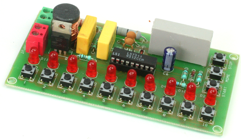
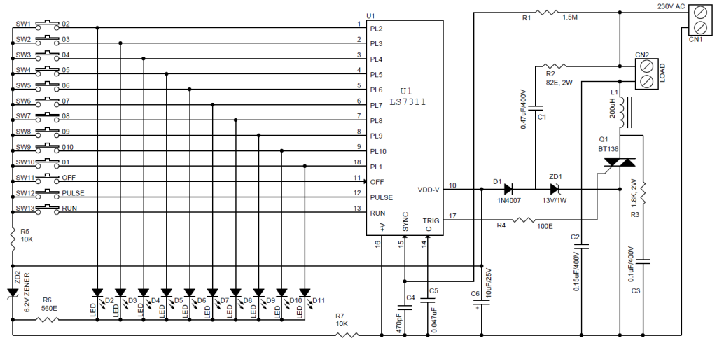
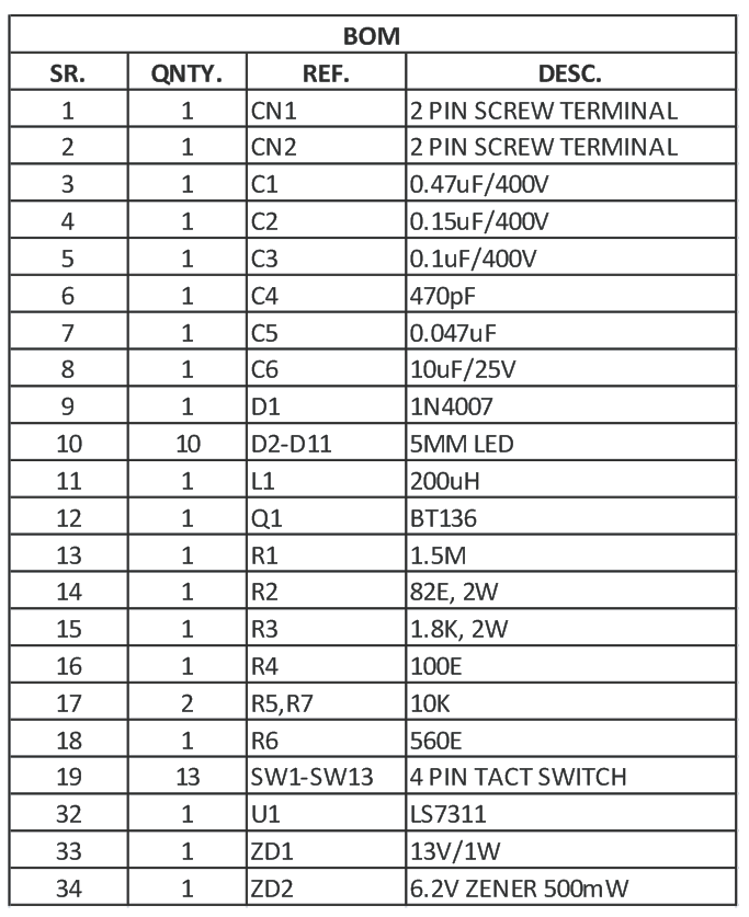
The project was specifically designed for motor speed control applications in appliances such as blenders, etc. Tact switches provided for selecting/indicating from 1 to 10 power levels ( Speed Levels). The project is ideal for universal and shaded-pole motor speed control for modern appliances design. Eliminates awkward mechanical switch assemblies and multi-taped motor winding.
I finished this laser wall trigger for my HIGH RESOLUTION AND ACCURACY CHRONOGRAPH. The purpose of this device is to generate the trigger start and stop impulses for my chronograph as soon as an object disrupts any of the laser beams.
LASER TRIGGER FOR CHRONOGRAPH – [Link]
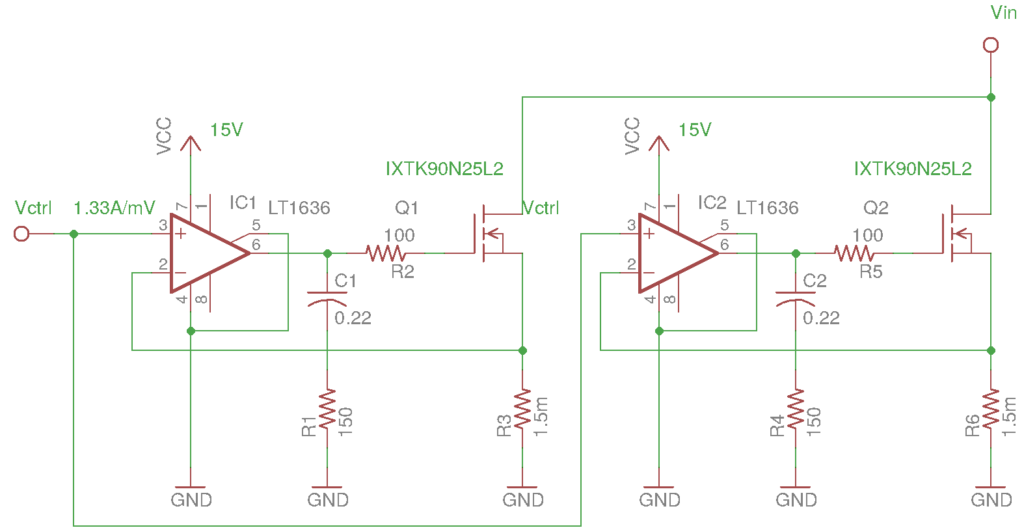
Kerry Wong built a 400W/100A electronic load using linear MOSFETs. He writes:
I bought a couple of IXYS linear MOSFETs (IXTK90N25L2) a while ago to test their capabilities when used as electronic load, and the result was quite impressive. So I decided to build another electronic load using both MOSFETs. As you can see in the video towards the end, this electronic load can sink more than 100 Amps of current while dissipating more than 400W continuously and can withstand more than 1kW of power dissipation in pulsed operation mode.
A 400W (1kW Peak) 100A Electronic Load Using Linear MOSFETs – [Link]
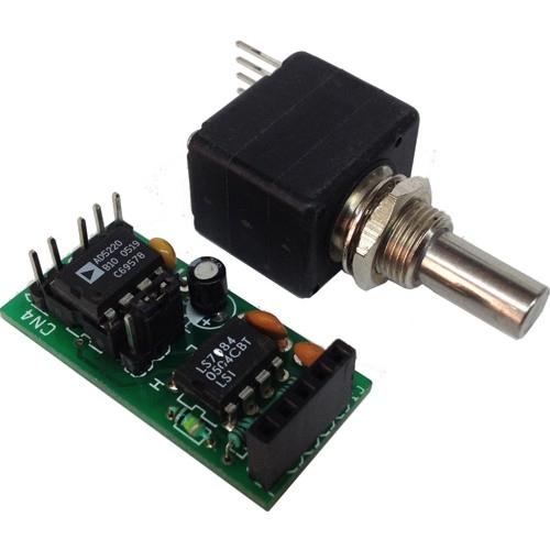
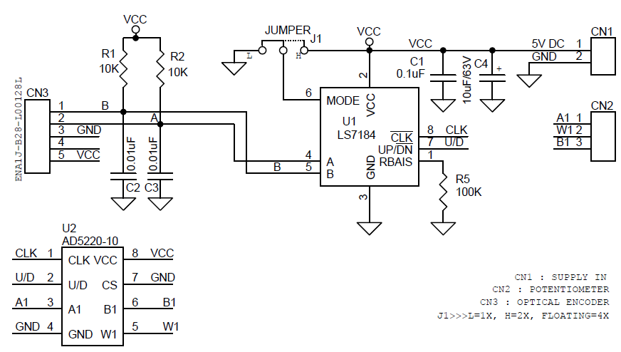
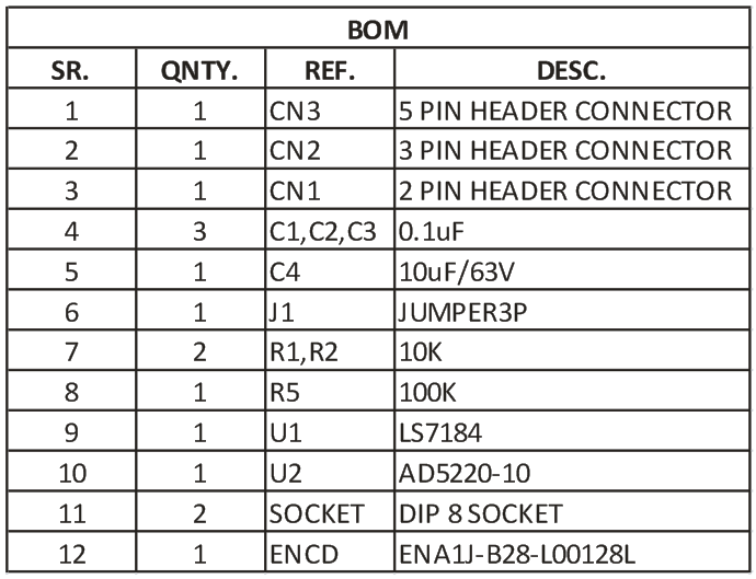
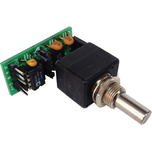
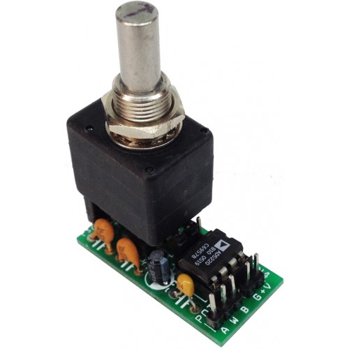
The primary application of the project is to replace the mechanical potentiometer with optical encoder which is long life, accurate, smooth in operation. The simple project has been designed around LS7184 quadrature clock converter IC from LSI semiconductor, AD5220-10 Digital potentiometer from Analog Devices, and optical encoder from Burns.
Quadrature clocks derived from optical encoder, when applied to the A and B inputs of the LS7184, are converted to strings of Clock and an Up/down direction control. These outputs interfaced directly to AD5220-10 Digital Potentiometer IC.
The AD5220-10 contains a single channel, 128 positions, and digitally-controlled 10K ohms variable resistor (VR) device. This device performs the same electronic adjustment function as a potentiometer.
Digital Potentiometer using Optical Encoder – 10KOhms – [Link]
The primary application of the project is to replace the mechanical potentiometer with optical encoder which is long life, accurate, smooth in operation. The simple project has been designed around LS7184 quadrature clock converter IC from LSI semiconductor, AD5220-10 Digital potentiometer from Analog Devices, and optical encoder from Burns.
Quadrature clocks derived from optical encoder, when applied to the A and B inputs of the LS7184, are converted to strings of Clock and an Up/down direction control. These outputs interfaced directly to AD5220-10 Digital Potentiometer IC.
The AD5220-10 contains a single channel, 128 positions, and digitally-controlled 10K ohms variable resistor (VR) device. This device performs the same electronic adjustment function as a potentiometer.
Jumper J1 provided for scale of the 3-state input to select resolution x1, x2 or x4. The input quadrature clock rate is multiplied by factors of 1, 2 and 4 in x1, x2 and x4 mode, respectively, in producing the output UP/DN clocks. x1, x2 and x4 modes selected by the MODE input logic.
levels are as follows:
Features
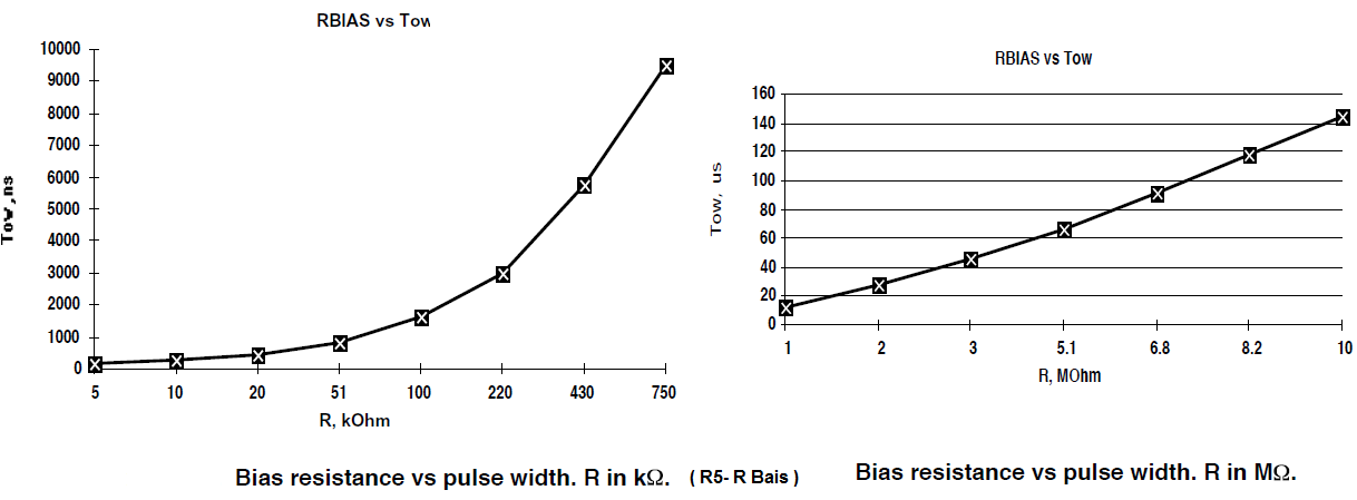
Note : Input for external component connection. A Resistor (R5) connected between this input and VSS adjusts the output clock pulse width (Tow). Refer to graph for appropriate bias resistor value.
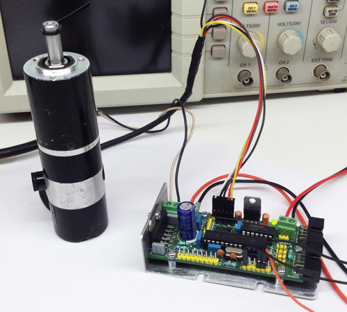
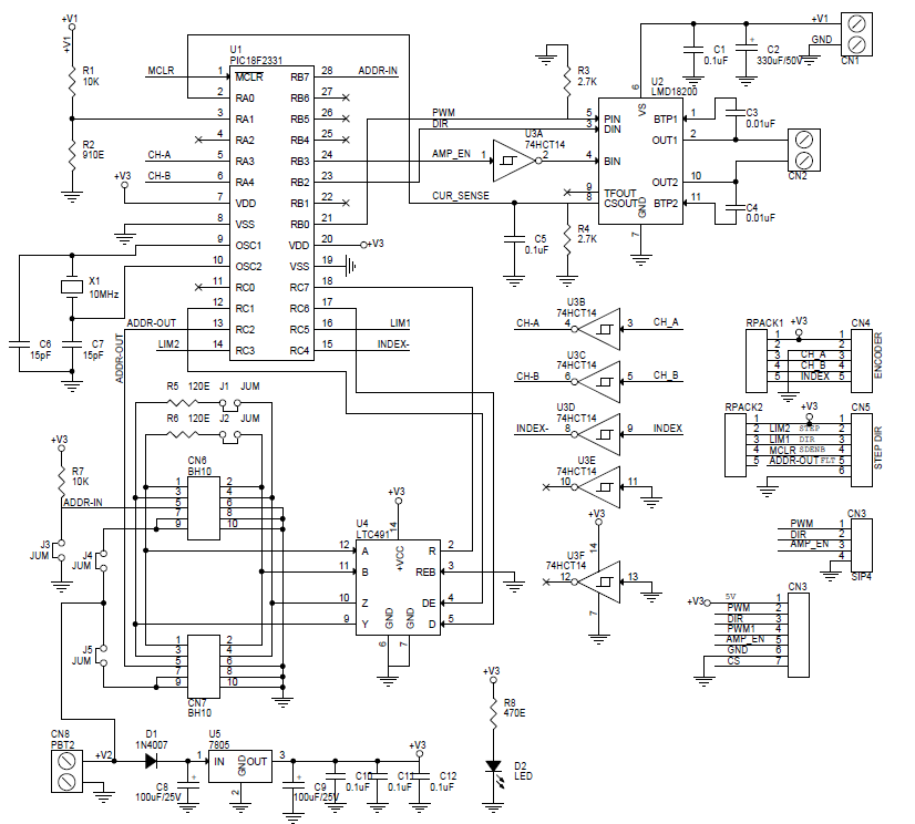
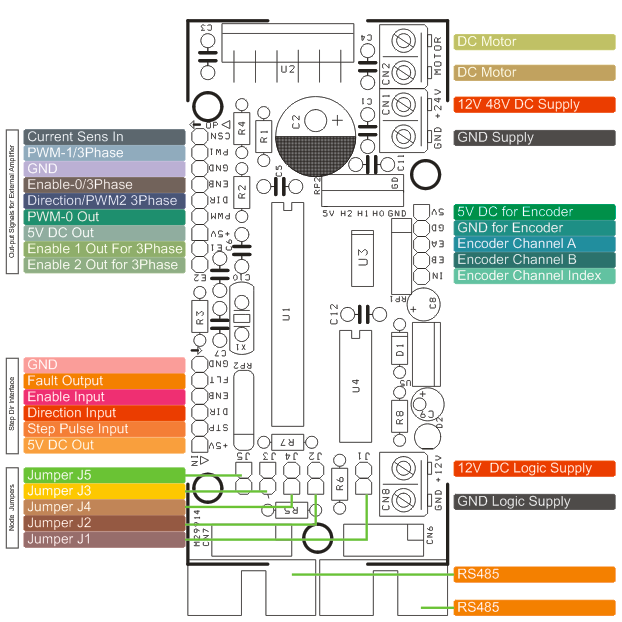
The SERVO Motion Control Board is maybe the fastest and lowest-cost way of getting your DC servo motor up and running. The clear, explicit documentation and the Windows test utility program take the mystery out of servo motor control. The board is designed for easily adding additional axes of control without flipping dip switches or setting jumpers. By mounting these compact, modular boards near your motors, you can greatly simplify the rat’s nest of wiring which plagues most multi-axis control systems. The PIC-SERVO SC Motion Control Board also includes motor power monitoring, soft current limiting, and position error limiting which eliminate the need for an additional real-time processor. If used with the RS232-485 Serial Adapter or with a Step & Direction signal generator, a set of SERVO Motion Controllers can even be operated as a stand-alone control system. All this comes at a price comparable to stepper motor controllers.
IC DATA SHEET & DRIVING SOFTWARE , TUNING SOFTWARE