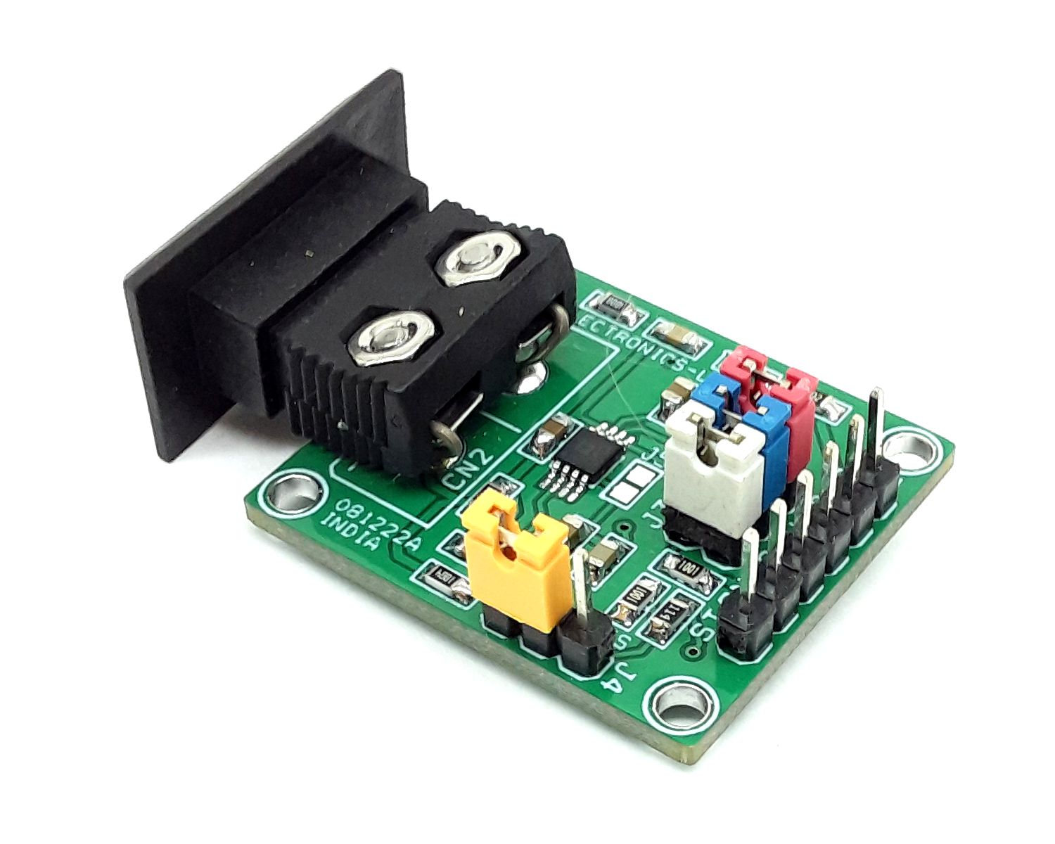
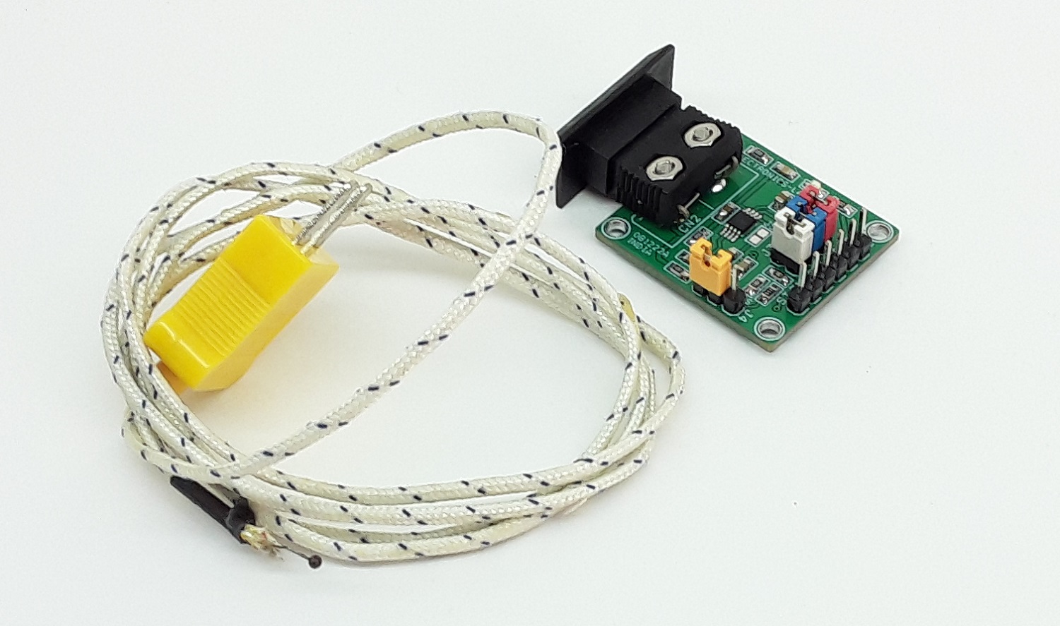
This Thermocouple Amplifier project provides a simple, low-cost solution for measuring thermocouple temperature. This board simplifies many of the difficulties of measuring thermocouples output. An integrated temperature sensor performs cold junction compensation. A fixed-gain instrumentation amplifier amplifies the small thermocouple voltage to provide a 5 mV/°C output. The high common-mode rejection of the amplifier blocks common-mode noise that the long thermocouple leads can pick up. For additional protection, the high impedance inputs of the amplifier make it easy to add extra filtering. The module can be used as standalone thermometers or as switched output setpoint controllers using either a fixed or remote setpoint control. The module can be powered from a single-ended supply (less than 3V) and can measure temperatures below 0°C by offsetting the reference input. To minimize self-heating, an unloaded AD8495 typically operates with a total supply current of 180 μA, but it is also capable of delivering in excess of ±5 mA to a load. The board can be interfaced with K-type (chromel-alumel) thermocouples. With an operating single supply of 5V, the 5 mV/°C output allows the devices to cover nearly 1000 degrees of a thermocouple’s temperature range. The project can also work with 3V supplies, allowing them to interface directly with lower-supply ADCs. They can also work with supplies as large as 36V in industrial systems that require a wide common-mode input range. The AD8495 cold junction compensation is optimized for operation in a lab environment, where the ambient temperature is around 25°C. The AD8495 is specified for an ambient range of 0°C to 50°C.
Features
- Supply Dual 5V DC (+/-5V DC)
- Low cost and easy to use
- Measurement Temperature Range −25°C to +400°C
- ±2°C Accuracy Temperature Ranges
- Pretrimmed for K-type thermocouples
- Internal cold junction compensation
- High-impedance differential input
- Standalone 5 mV/°C thermometer
- Reference pin allows offset adjustment
- Mode: Linear, Set Point Controller, Hysteresis on Setpoint Controller, Selection Using Jumpers
- Thermocouple break detection
- On Board Power LED
- 4 x 2.5mm Mounting Holes
- PCB Dimensions 31.12 x 27.31mm
Applications
- K-type thermocouple temperature measurement
- Setpoint controller
- Celsius thermometer
- Universal cold junction compensator
- White goods (oven, stove top) temperature measurements
- Exhaust gas temperature sensing
- Catalytic converter temperature sensing
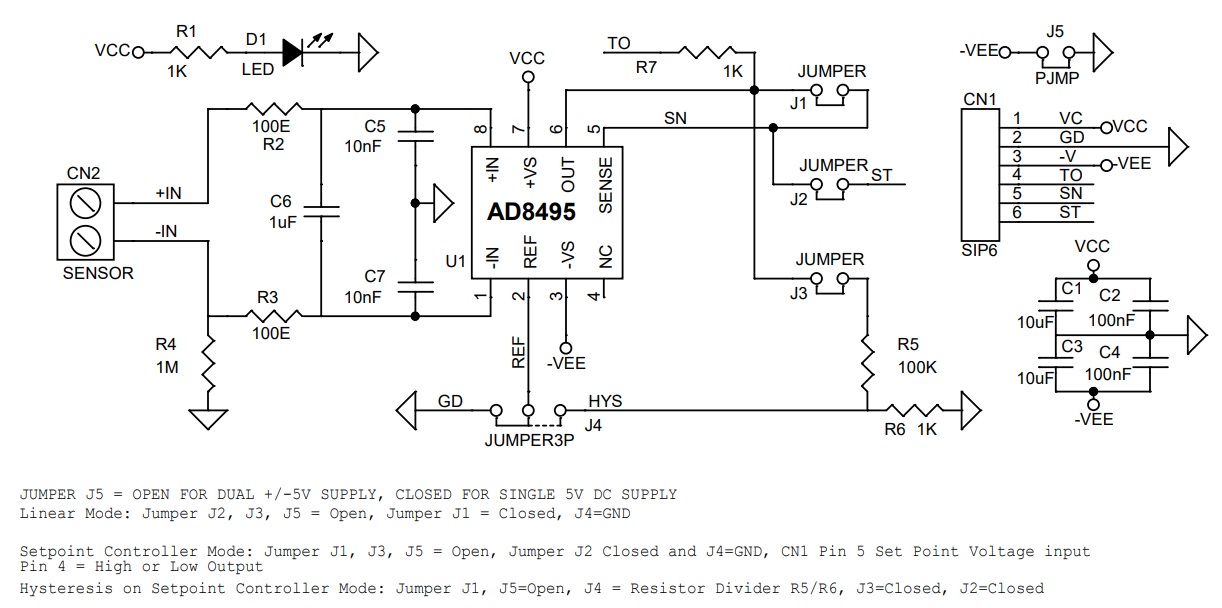
The board is designed to allow users to quickly prototype the precision thermocouple amplifiers for various user-defined configurations for different applications. The circuit has three modes of operation: linear mode, setpoint controller mode, and hysteresis on setpoint controller mode. Various modes can be set using onboard jumpers.
Linear Mode: Jumper J2, J3, J5 = Open, Jumper J1 = Closed, J4=GND
The linear mode can be selected by closing Jumper J1 and J4 = GND linear, the output voltage of the AD8495 is calculated as follows:
VOUT = (T_MJ × 5 mV/°C) + VREF
where T_MJ is the thermocouple measurement junction temperature.
Setpoint Controller Mode: Jumper J1, J3, J5 = Open, Jumper J2 Closed and J4=GND, CN1 Pin 5 Set Point Voltage input, Pin 4 = High or Low Output
The board operates as a temperature setpoint controller when configured with either a thermocouple input from a remote location or with the AD8495 being used as a temperature sensor. When the measured temperature is below the setpoint temperature, the output voltage goes to −VS. When the measured temperature is above the setpoint temperature, the output voltage goes to +VCC. For optimal accuracy and common mode rejection ratio (CMRR) performance, the setpoint voltage must be created with a low-impedance source. If the setpoint voltage is generated with a voltage divider, a buffer is recommended.
Hysteresis on Setpoint Controller Mode: Jumper J1, J5=Open, J4 = Resistor Divider R5/R6, J3=Closed, J2=Closed
Hysteresis can be added to the setpoint controller by using a resistor R5, R6 divider from the output to the reference pin, The resistors installed on the board are 1 kΩ and 100 kΩ, which creates a window of approximately 10°C around the setpoint temperature for a +VCC of 5 V.
Measuring Negative Temperatures
The board can measure negative temperatures using either single or dual supplies. When operating on dual supplies with the J4 jumper = GND position (reference pin grounded), a negative output voltage indicates a negative temperature at the thermocouple measurement junction. When operating the board series evaluation board on a single supply level, apply a positive voltage (less than +VS) on the reference pin to shift the output. The jumper from J2 must be removed so that the reference pin is not grounded. An output voltage less than VREF indicates a negative temperature at the thermocouple measurement junction.
Thermocouple Break Detection
The board offers open thermocouple detection. The inputs of the AD8495 are PNP type transistors, which means that the bias current always flows out of the inputs. Therefore, the input bias current drives any unconnected input high, which rails the output. Resistor R4 connected to GND causes the AD8495 output to rail high in an open thermocouple condition.
Gain Error
Gain error is the amount of additional error when measuring away from the measurement junction calibration point. For example, if the part is calibrated at 25°C and the measurement junction is 100°C with a gain error of 0.1%, the gain error contribution is (100°C − 25°C) × (0.1%) = 0.075°C. This error can be calibrated with a two-point calibration if needed, but it is usually small enough to ignore.
Ambient Temperature Rejection
The specified ambient temperature rejection represents the ability of the AD8495 to reject errors caused by changes in the ambient temperature/reference junction. For example, with 0.025°C/°C ambient temperature rejection, a 20°C change in the reference junction temperature adds less than 0.5°C error to the measurement.
Input Voltage Protection
The board has very robust inputs. Input voltages can be up to 25 V from the opposite supply rail. For example, with a +5 V positive supply and a −3 V negative supply, the board can safely withstand voltages at the inputs from −20 V to +22 V. Voltages at the reference and sense pins should not go beyond 0.3 V of the supply rails.
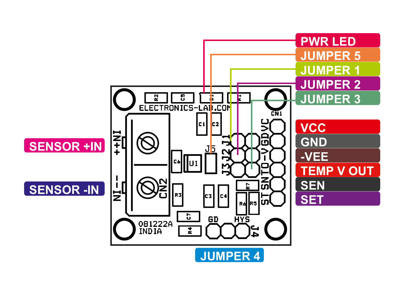
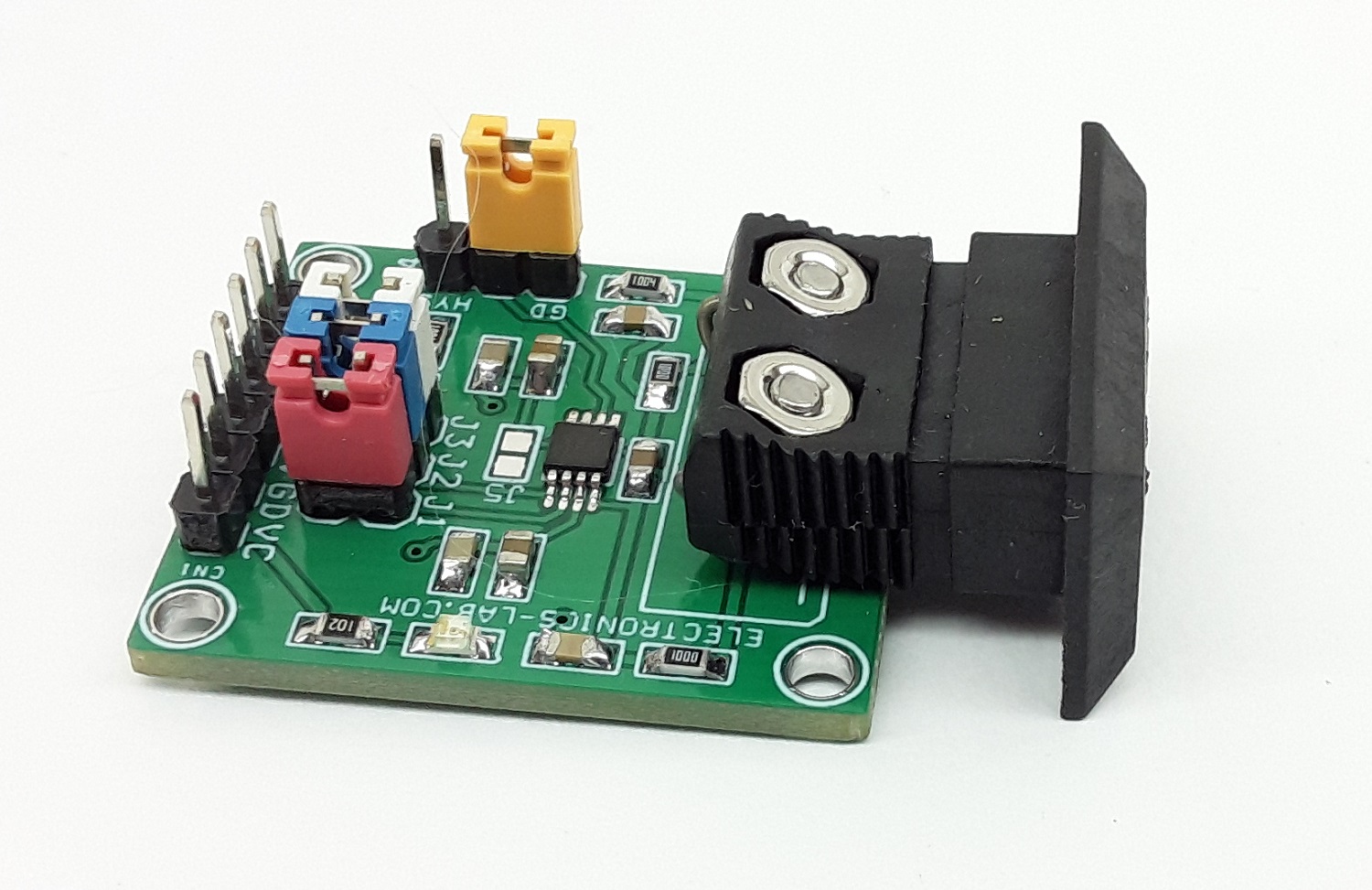
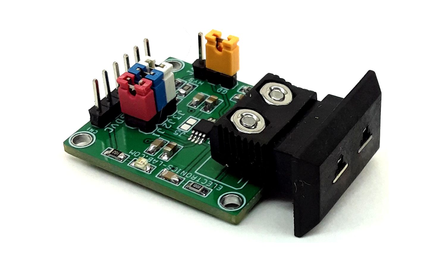
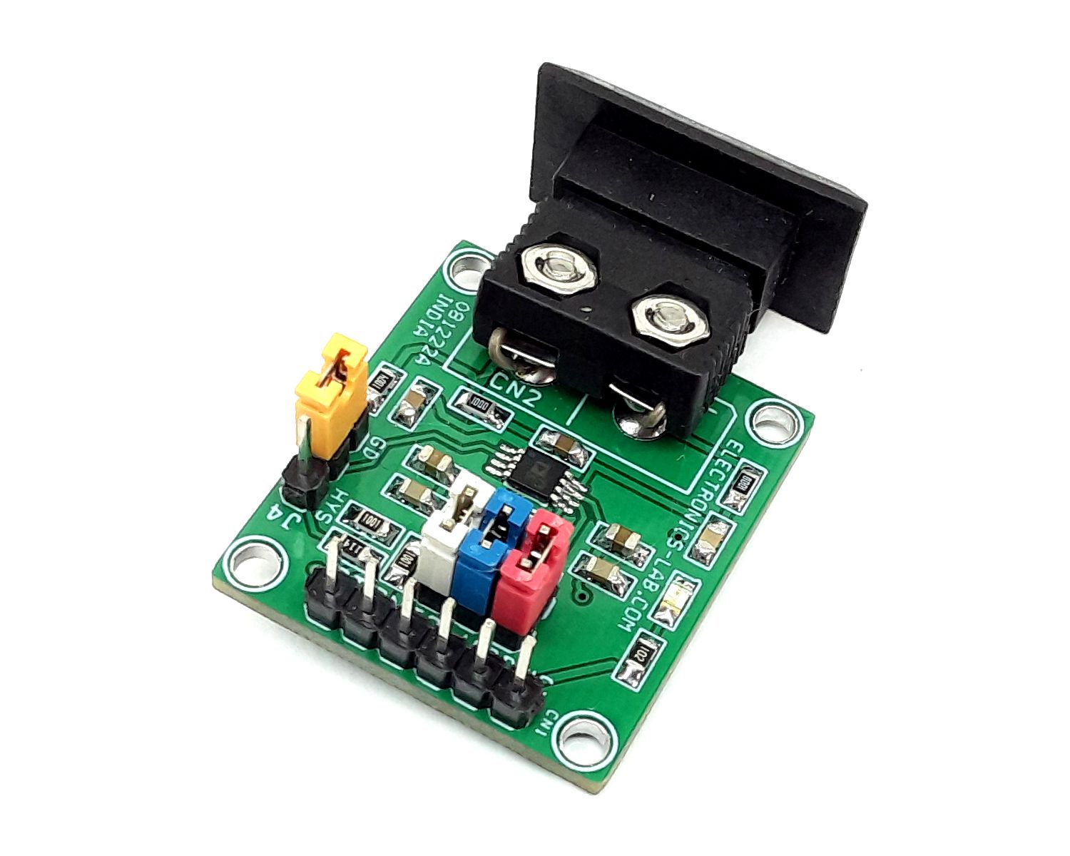
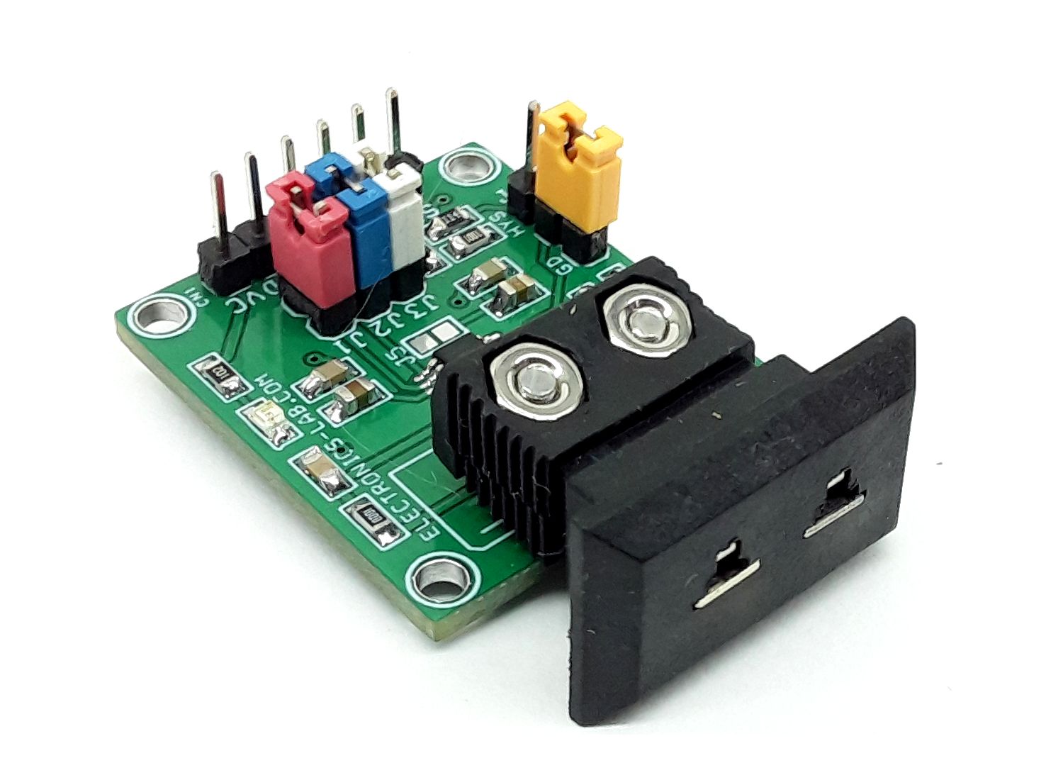
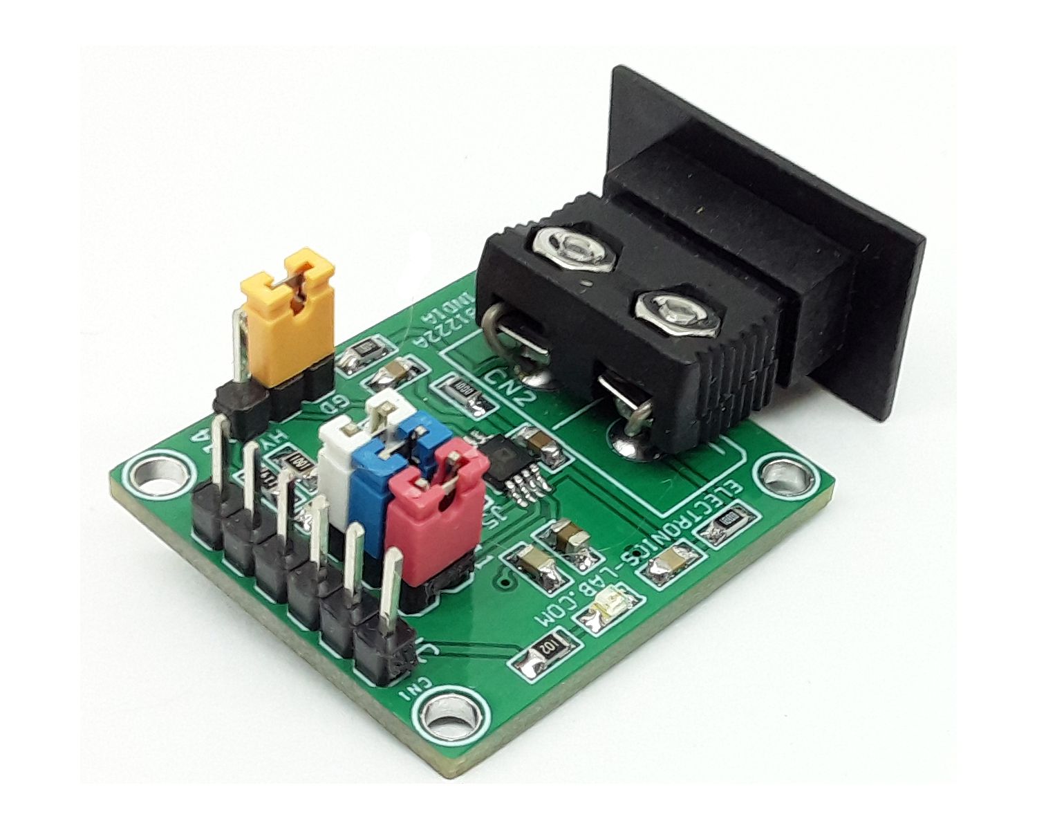
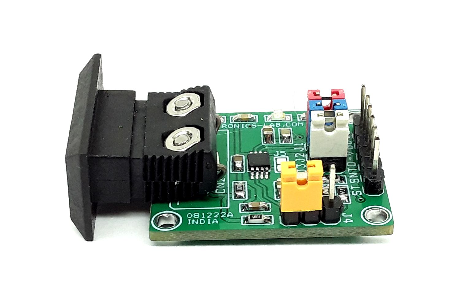
Connections and Other Details
- CN1: Pin 1 = VCC +5V DC, Pin 2 = GND, Pin 3 = -VEE -5V, Pin 4 Temperature V-Output, Pin 5 = Sense (No Use), Pin 6 = Set Point V-Input
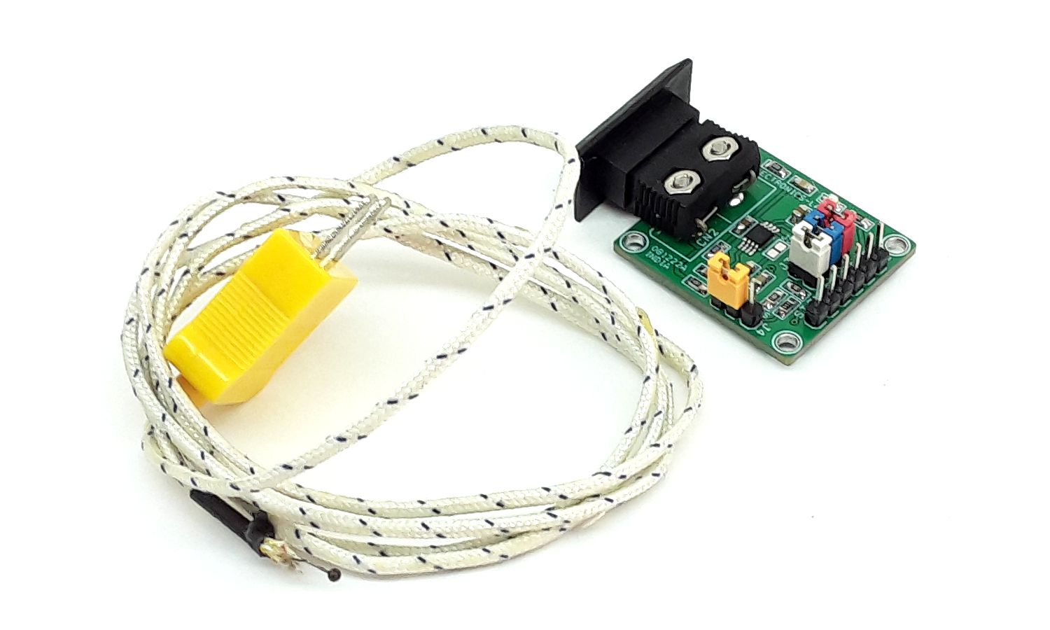
- CN2: Pin 1 = K Type Sensor + Input, Pin 2 = Sensor -Input
- Jumper J1: For Set the Linear Output
- Jumper J2: For Set Point Input Mode
- Jumper J3: For Hysteresis on Setpoint Controller Mode
- Jumper J4: For Reference Ground or Hysteresis Selection
- Jumper J5: Closed for Single Supply Input, Open for Dual Power Supply Input (Solder Jumper)
Schematic
Parts List
| NO. | QNTY. | REF. | DESC. | MANUFACTURE | SUPPLIER | SUPPLIER PART NO |
|---|---|---|---|---|---|---|
| 1 | 1 | CN1 | 6 PIN MALE HEADER PITCH 2.54MM | WURTH | DIGIKEY | 732-5319-ND |
| 2 | 1 | CN2 | TEMPERETURE SENSOR CONNECTOR | LABFACILITY | ELEMENT14 | 3810628 |
| 3 | 2 | C1,C3 | 10uF/16V CERAMIC SMD SIZE 0805 | YAGEO/MURATA | DIGIKEY | |
| 4 | 2 | C2,C4 | 100nF/50V CERAMIC SMD SIZE 0805 | YAGEO/MURATA | DIGIKEY | |
| 5 | 2 | C5,C7 | 10nF/50V CERAMIC SMD SIZE 0805 | YAGEO/MURATA | DIGIKEY | |
| 6 | 1 | C6 | 1uF/25V CERAMIC SMD SIZE 0805 | YAGEO/MURATA | DIGIKEY | |
| 7 | 1 | D1 | LED RED SMD SIZE 0805 | OSRAM | DIGIKEY | 75-1278-1-ND |
| 8 | 3 | J1,J2,J3 | JUMPER- 2 PIN MALE HEADER PITCH 2.54MM | WURTH | DIGIKEY | 732-5315-ND |
| 9 | 1 | J4 | JUMPER-3PIN MALE HEADER PITCH 2.54MM | WURTH | DIGIKEY | 732-5316-ND |
| 10 | 1 | J5 | PJMP-PCB SOLDER JUMPER | |||
| 11 | 3 | R1,R6,R7 | 1K 1% SMD SIZE 0805 | YAGEO/MURATA | DIGIKEY | |
| 12 | 2 | R2,R3 | 100E 1% SMD SIZE 0805 | YAGEO/MURATA | DIGIKEY | |
| 13 | 1 | R4 | 1M 1% SMD SIZE 0805 | YAGEO/MURATA | DIGIKEY | |
| 14 | 1 | R5 | 100K 1% SMD SIZE 0805 | YAGEO/MURATA | DIGIKEY | |
| 15 | 1 | U1 | AD8495 SOIC8 | ANALOG DEVICES | DIGIKEY | AD8495ARMZ-R7CT-ND |
| 16 | 4 | SHUNT | SHUNT-JUMPER | SULLINS CONNCT | DIGIKEY | S9001-ND |
Connections
Gerber View
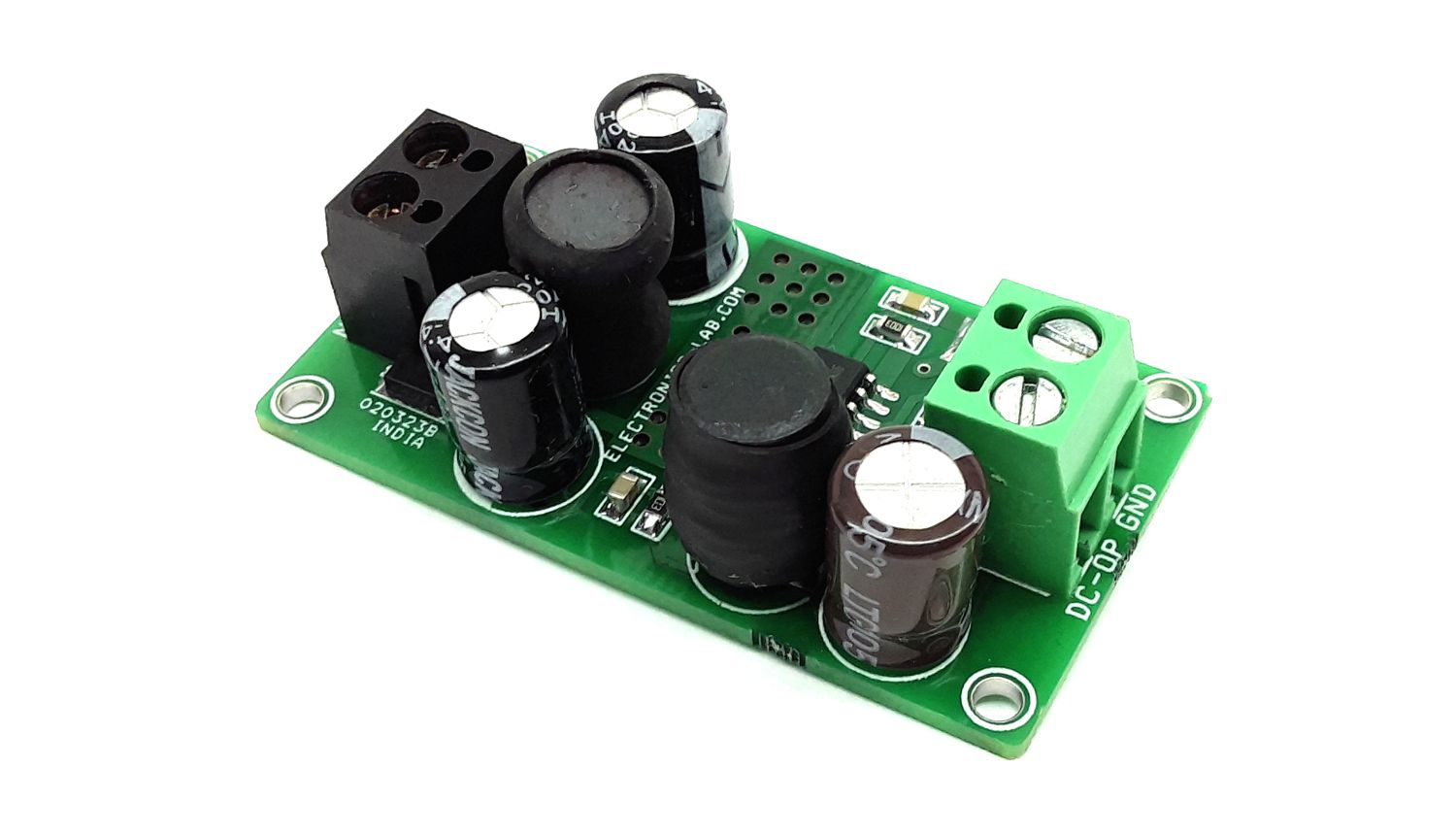
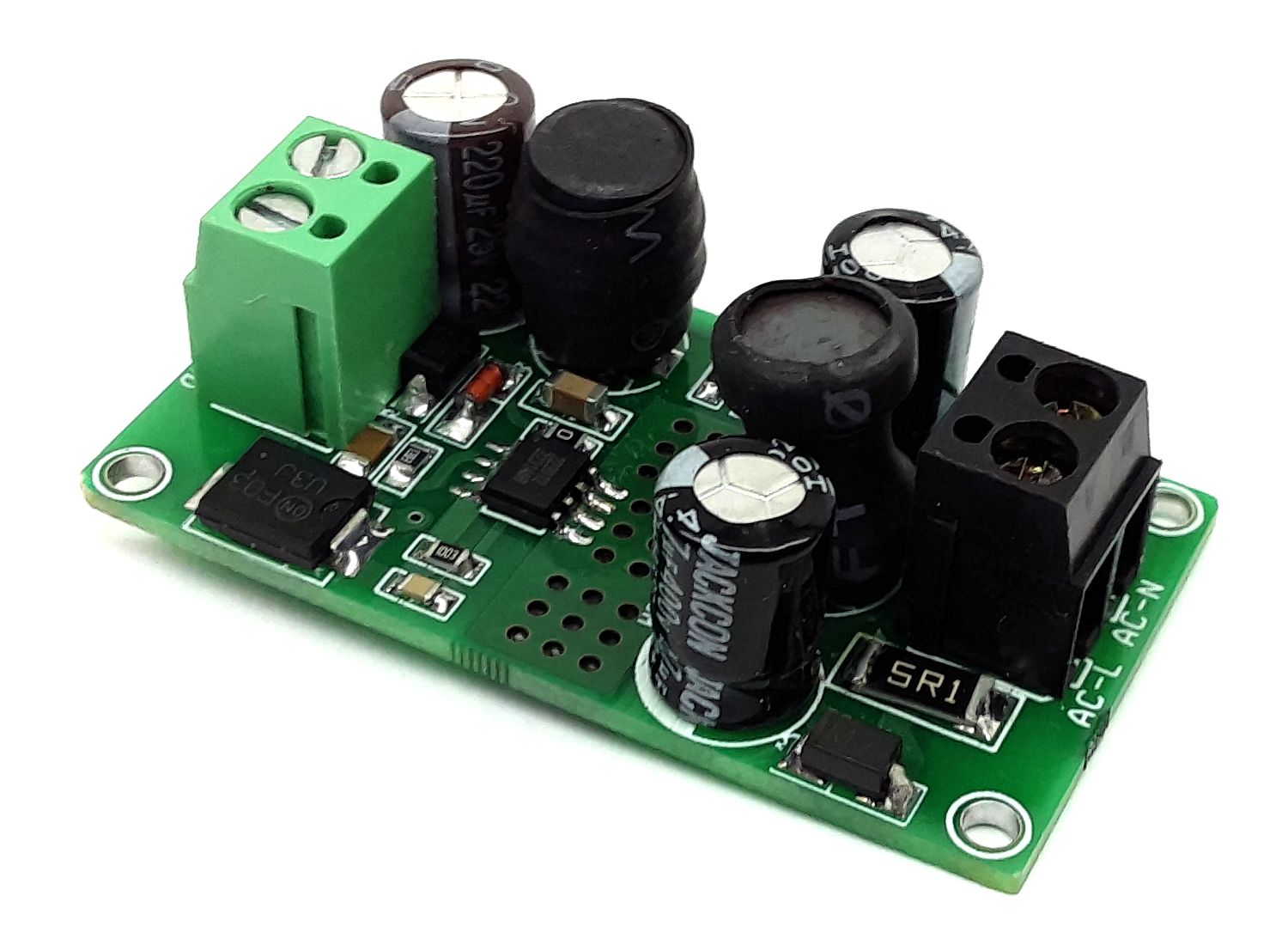
Photos
Video


 With a strong