The project presented here is a dual 12-bit PWM-to-voltage output DAC with high accuracy. The board is based on the LTC2644 chip. The LTC2644 measures the period and pulse width of the PWM input signals and updates the voltage output DACs after each corresponding PWM input rising edge. The DAC outputs update and settle to 12-bit accuracy within 8μs typically and are capable of sourcing and sinking up to 5mA (3V) or 10mA (5V), eliminating voltage ripple and replacing slow analog filters and buffer amplifiers. The circuit has a full-scale output of 2.5V using the 10ppm/°C internal reference. It can operate with an external reference, which sets the full-scale output equal to the external reference voltage. Each DAC enters a pin-selectable idle state when the PWM input is held unchanged for more than 60ms. The project operates from a single 2.7V to 5.5V supply and supports PWM input voltages from 1.71V to 5.5V. The PWM frequency can be any frequency between 30Hz and 6. 25kHz. The input level can be between 1.71V and 5.5V, set by a separate IOVCC pin. This project solves many problems associated with filtering a PWM signal to produce an analog voltage, producing a fast-settling, accurate analog voltage in response to a digital PWM input.
Features
- Supply 5V (Range 2.7V to 5.5V)
- Current Consumption approx. 15mA
- Input PWM Signal Level Can be Between 1.71V and 5.5V
- 2 Channel Input and Output
- Input PWM Frequency 30Hz to 6.25Khz
- Output 0 to 2.5V (0 to 99% Duty Cycle)
- On Board Power LED
- Header Connector for Inputs and Outputs
- Jumper For Power Down
- Jumper for Internal Reference or External Reference
- Jumper for Idle Mode
- Jumper for IOVC
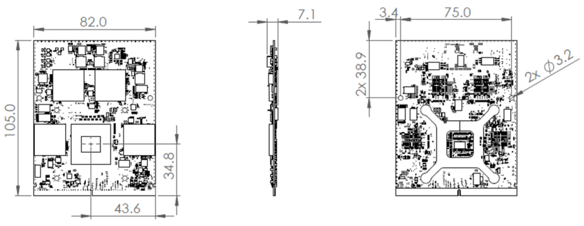
- PCB Dimensions 31.43 x 22.86 mm
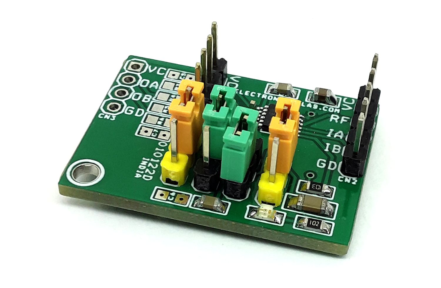
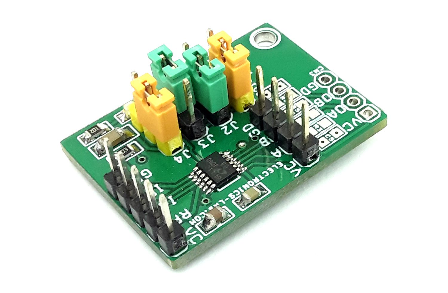
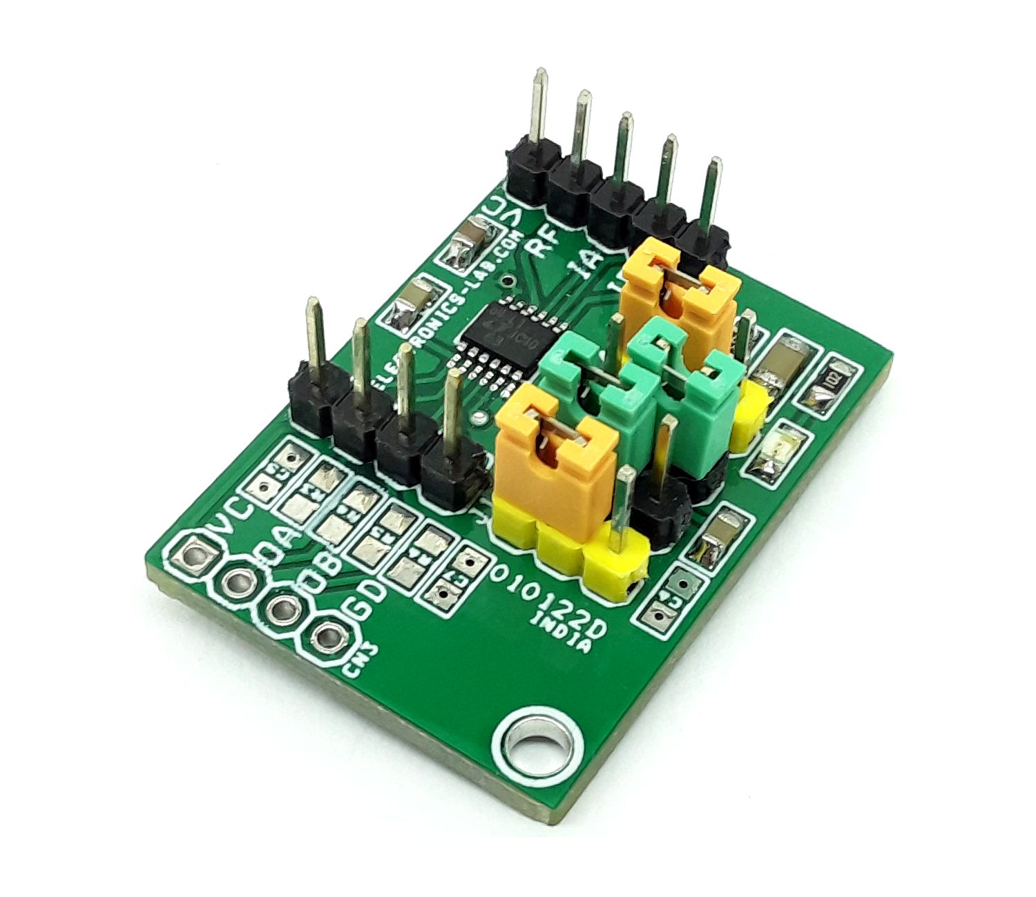
Standalone Operation
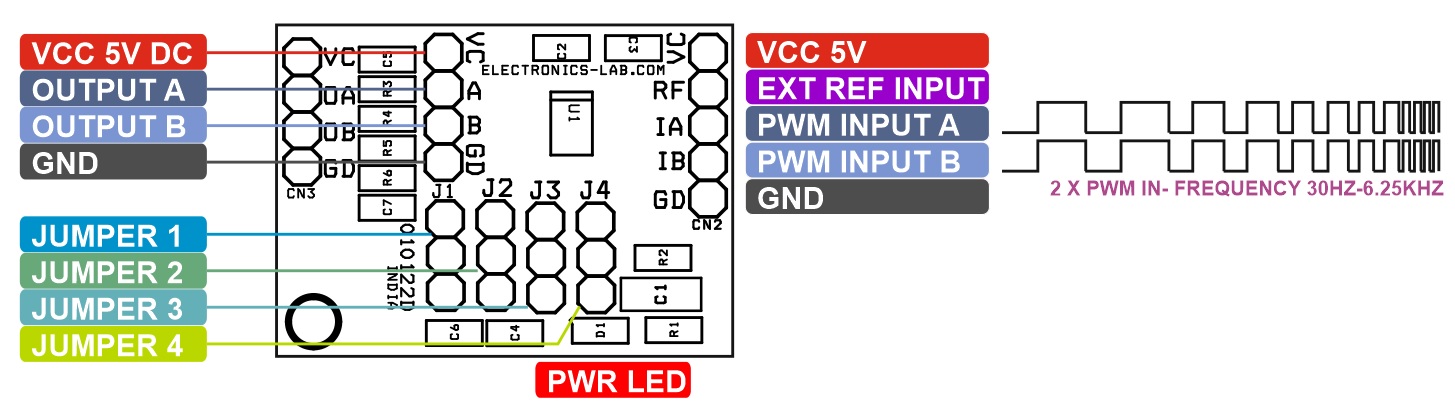
For standalone operation. Connect a 2.7V to 5.5V supply to the VCC and a GND of CN1 Pin 1 and Pin 4. Connect the IOVCC(IOV) to VCC using Jumper J2 such that the input logic level matches the VCC supply. If a different logic level is required, remove the IOVCC(IOV) jumper and connect the middle pin2 of J2 to a supply equal to the PWM signals’ logic level to the IOVCC(IOV) and GND. There is no sequencing requirement between VCC and IOVCC. Any convenient PWM source can be used to convert the PWM signal into a voltage output.
Jumpers Settings
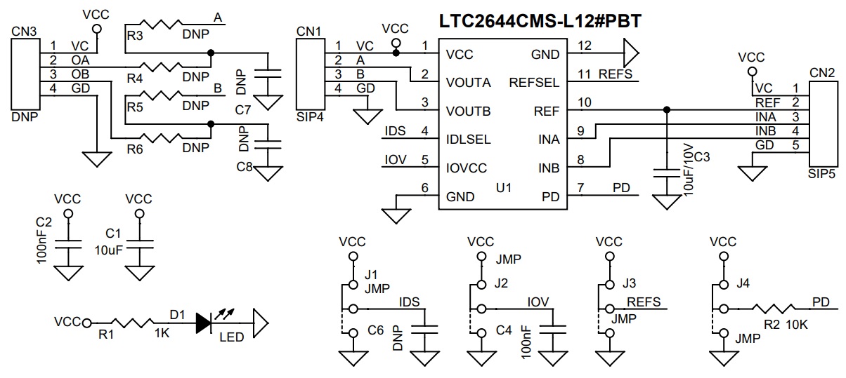
- Jumper J1 (Idle Mode Select Input): Connecting this jumper to VCC or GND determines the DAC behavior when the PWM input remains high or low for more than the Idle Mode Timeout time (50ms minimum, 70ms maximum). When set to VCC (High), a low level on a PWM input will set the DAC output to a high impedance state. A high level will cause the DAC output to hold its last value. When set to GND (Low), a low level on a PWM input will set the DAC output to zero-scale, and a high level will set the DAC output to full scale.
- Jumper J2: For normal operation Connect the IOVCC(IOV) to VCC using Jumper J2 such that the input logic level matches the VCC supply. If a different logic level is required, remove the IOVCC(IOV) jumper and connect the middle pin2 of J2 to a supply equal to the PWM signals’ logic level to the IOVCC(IOV) and GND.
- Jumper J3: Set to GND (default) to use the internal reference. Set to EXT to supply an external reference to the REF CN2 Pin 2.
- Jumper 4: Connect it to VCC for normal Operation, GND Power-Down.
REF: Reference Output/Input. When the REFSEL jumper is set to INT, the LTC2645’s internal reference can be measured at this point. Nominal impedance is 500Ω. If it is used to drive external circuits it must be buffered appropriately. When REFSEL is set to EXT using Jumper J3, an external reference between 1V and VCC may be connected to this point
LTC2644-L12: Supports Frequency up to 6.25Khz, for higher frequency select below chips.
- LTC2644-L12 Chip Supports 12Bit resolution, 30Hz to 6.25Khz input
- LTC2644-L10 Chip Supports 10Bit resolution, 30Hz to 25Khz input
- LTC2644-L8 Chip Supports 8 Bit resolution, 30Hz to 100Khz input
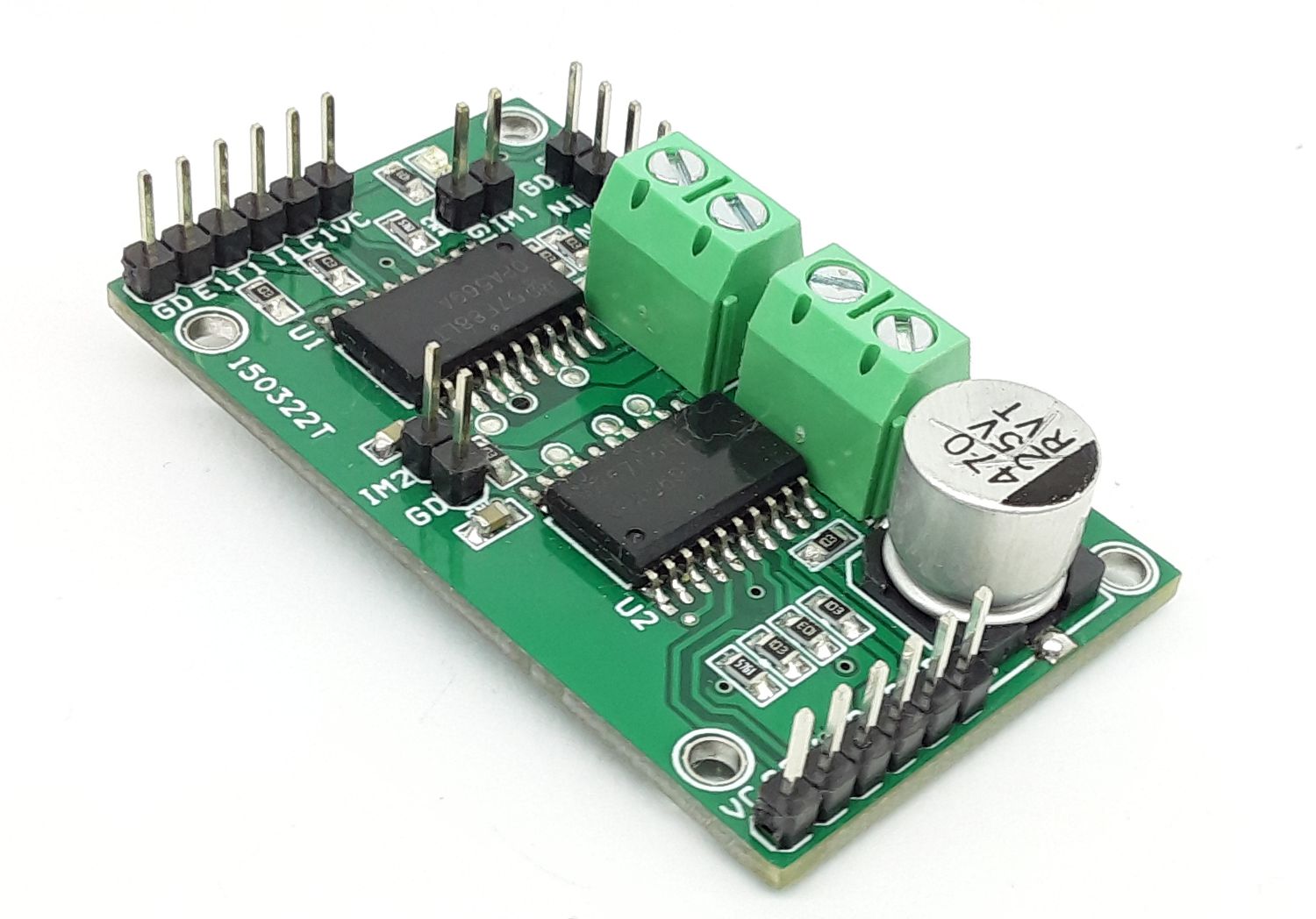
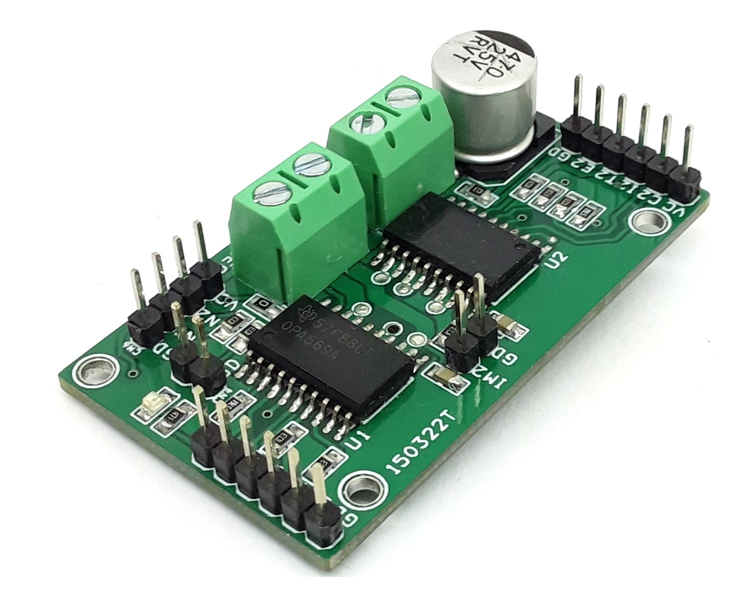
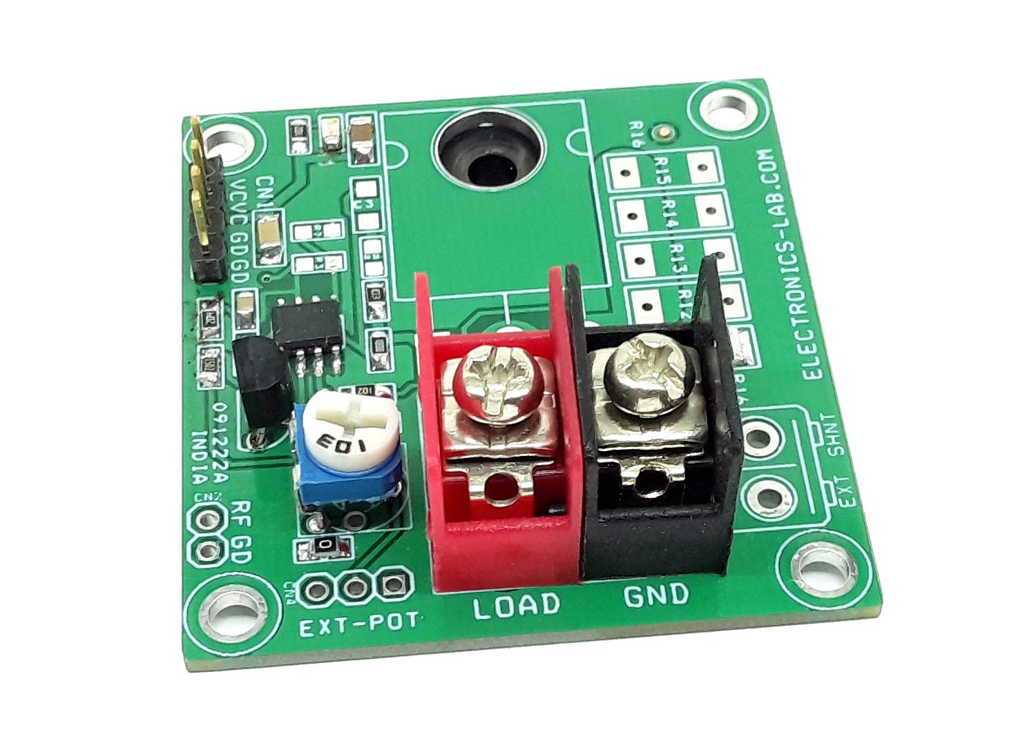
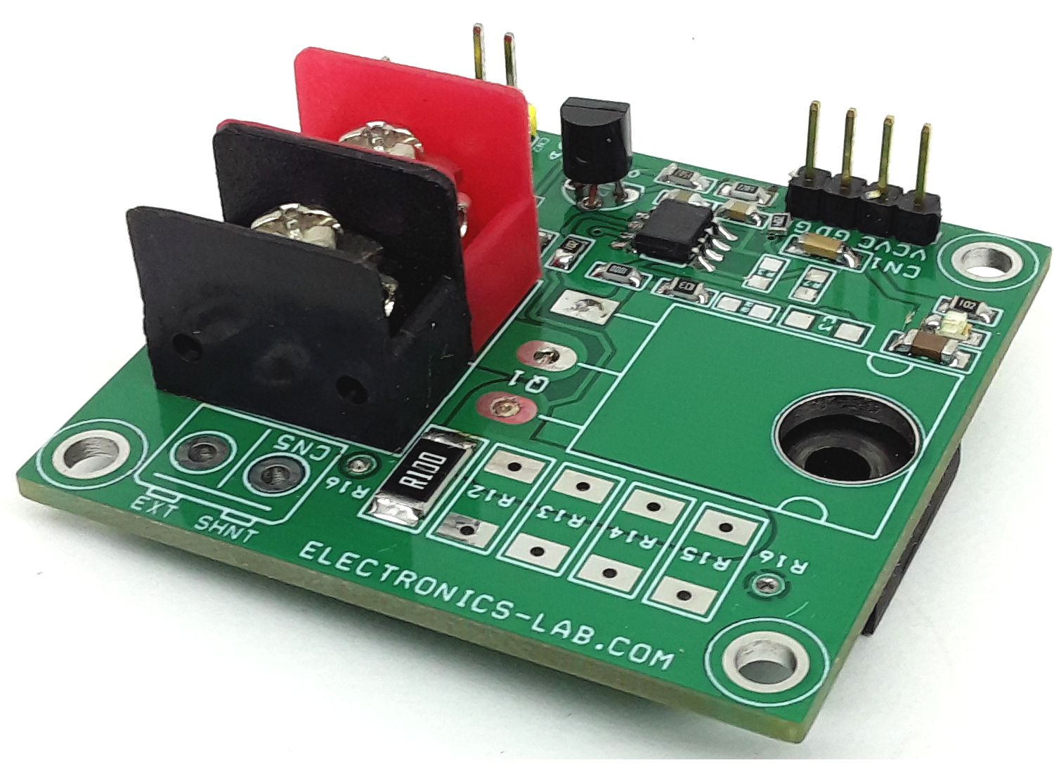
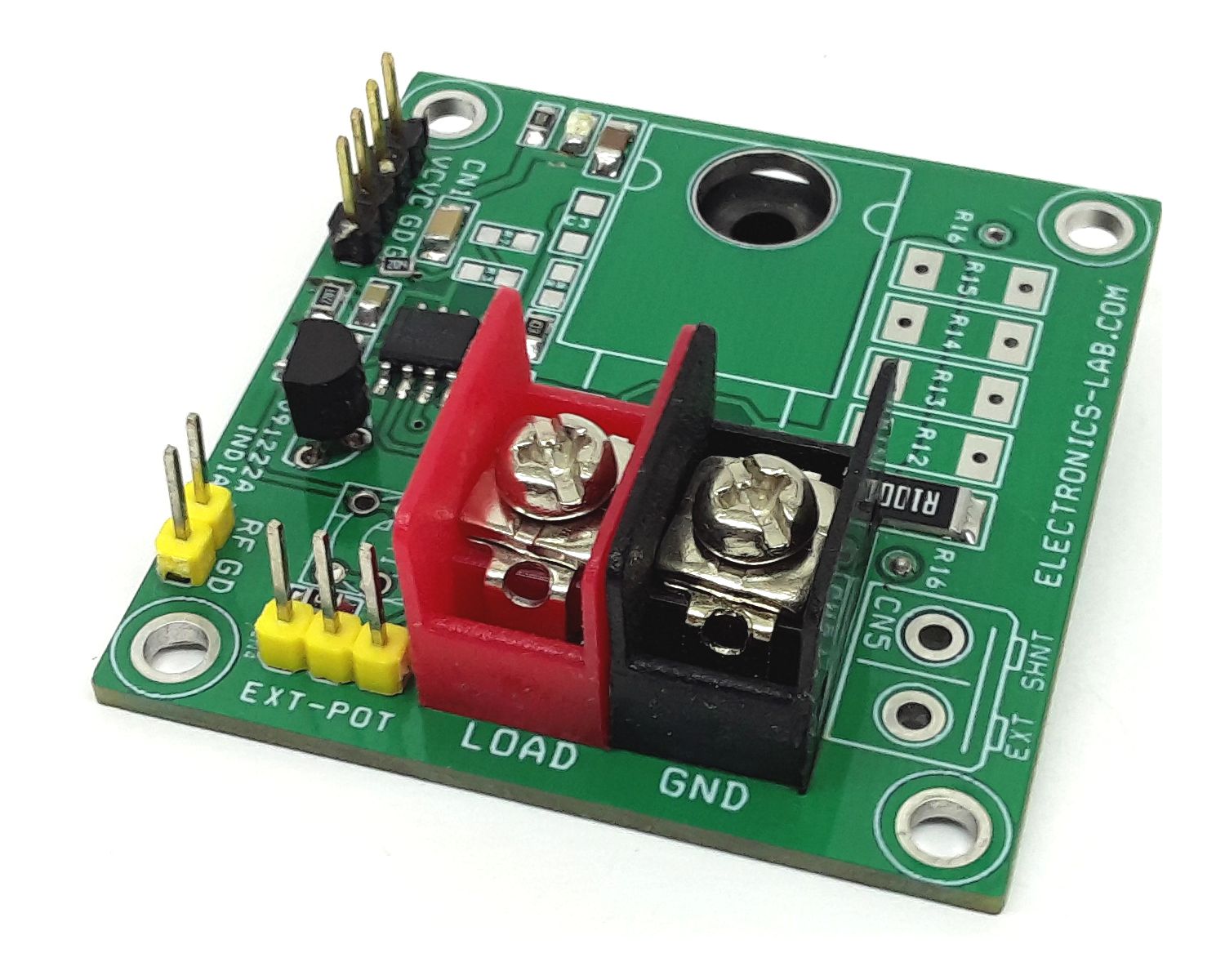
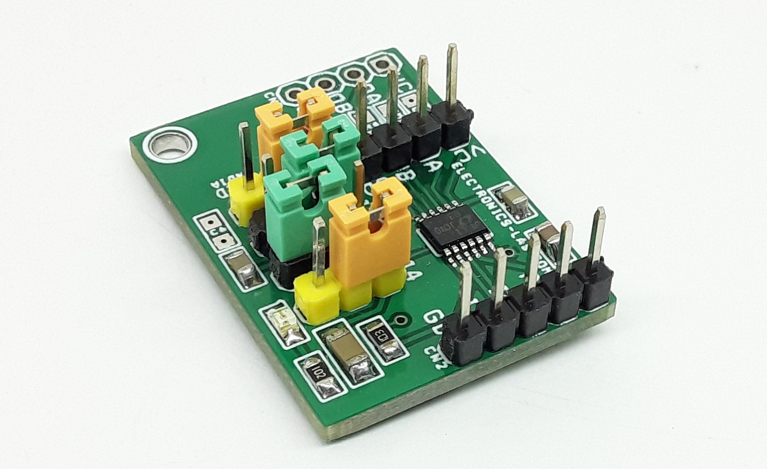
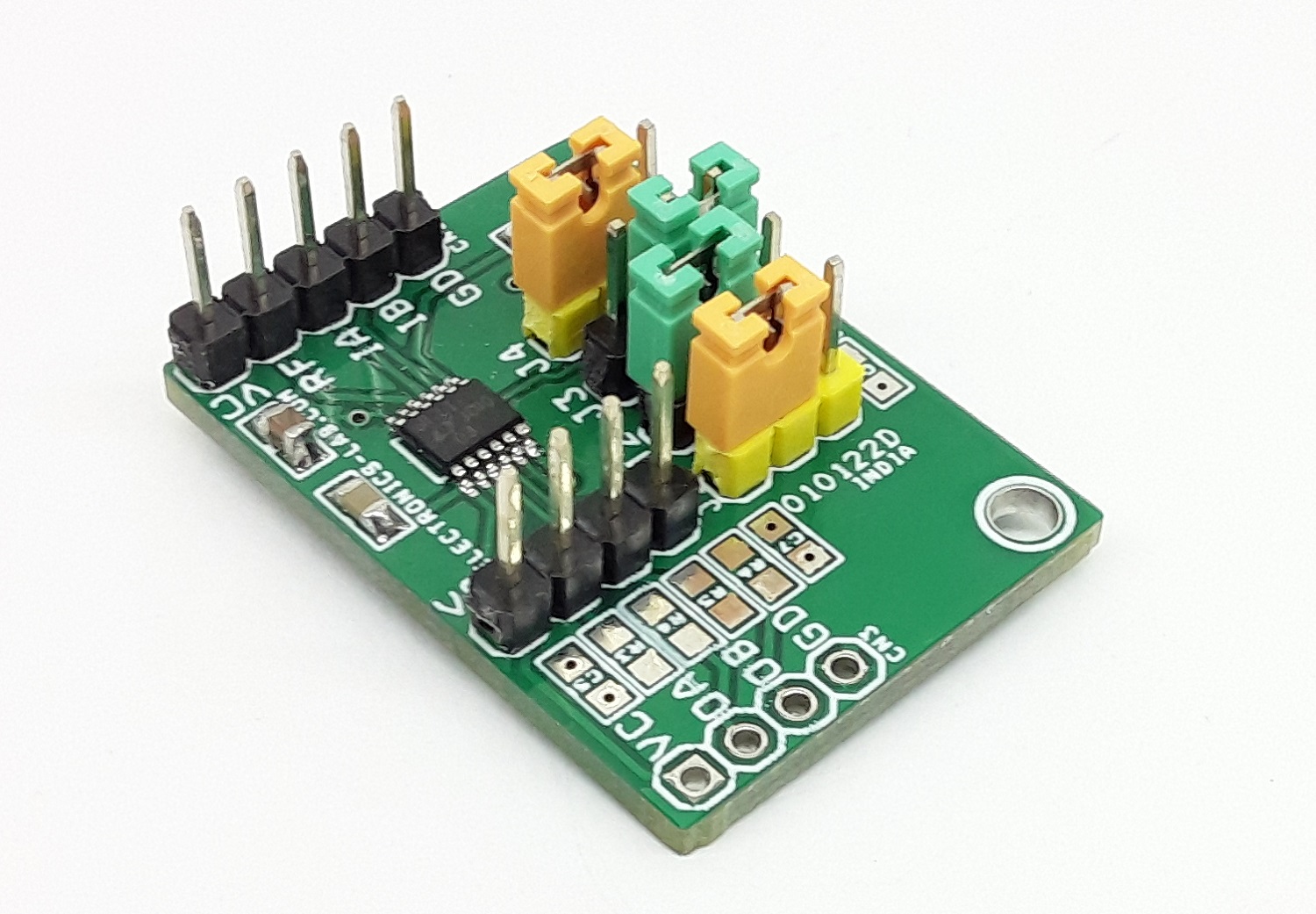
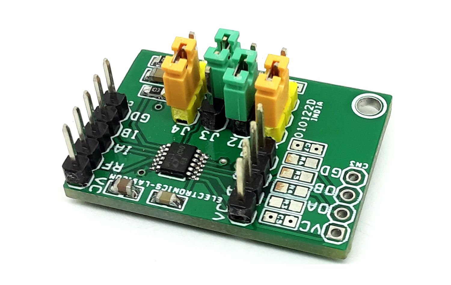
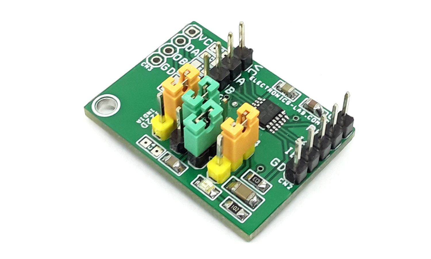
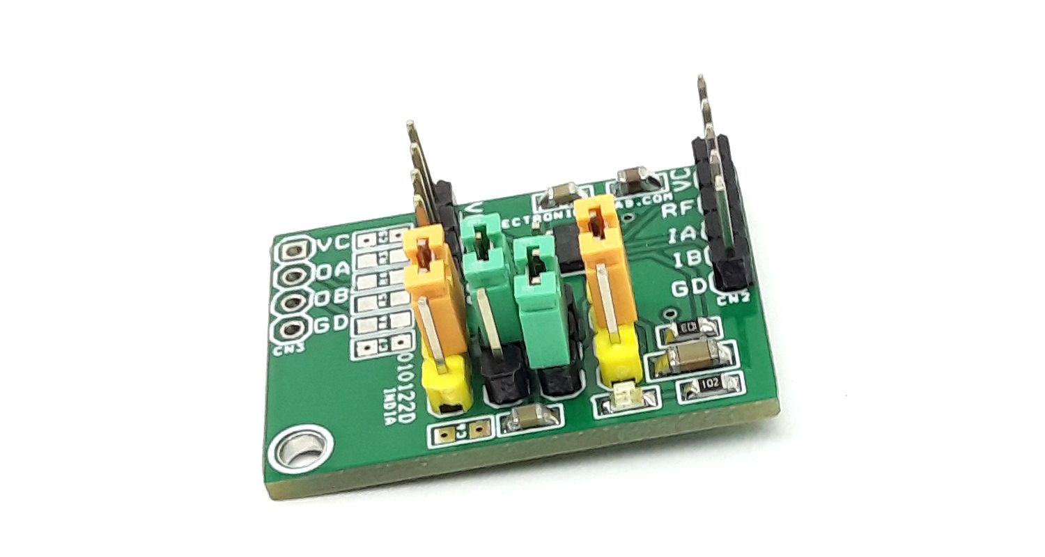
Connections and other details
- CN1: Pin 1 = VCC 5V DC, Pin 2 = Vout Channel A, Pin 3 = Vout Channel B , Pin 4 = GND
- CN2: Pin 1 = VCC 5V DC, Pin 2 = External Reference Optional, Pin 3 = PWM Input Channel A, Pin 4 = PWM Input Channel B
- Jumper 1 = IDLE Setting High/Low
- Jumper 2 = VCC for Standalone Operations Internal VCC
- Jumper 3 = Internal Reference or External Reference Selection, Connect it GND for Normal Operation
- Jumper 4 = Power Down, Connect it to VCC for Normal Operation, GND = Power Dow
- D1 Power LED
- CN3, R3, R4, R5, R6, C7, C8: Optional, can be used for output filter for smooth Output
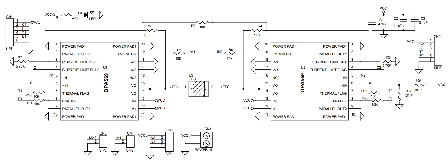
Schematic
Parts List
| NO. | QNTY. | DESC. | REF. | MANUFACTURER | SUPPLIER | SUPPLIER PART NO |
|---|---|---|---|---|---|---|
| 1 | 1 | CN1 | 4 PIN MALE HEADER PITCH 2.54MM | WURTH | DIGIKEY | 732-5317-ND |
| 2 | 1 | CN2 | 5 PIN MALE HEADER PITCH 2.54MM | WURTH | DIGIKEY | 732-5318-ND |
| 3 | 8 | R3,CN3,R4,R5,R6,C6,C7,C8 | DNP | |||
| 4 | 1 | C1 | 10uF/10V CERAMIC SMD SIZE 0805 | YAGEO/MUARATA | DIGIKEY | |
| 5 | 2 | C2,C4 | 100nF/25V CERAMIC SMD SIZE 0805 | YAGEO/MUARATA | DIGIKEY | |
| 6 | 1 | C3 | 10uF/10V CERAMIC SMD SIZE 0805 | YAGEO/MUARATA | DIGIKEY | |
| 7 | 1 | D1 | LED RED SMD SIZE 0805 | OSRAM | DIGIKEY | 475-1278-1-ND |
| 8 | 4 | J1,J2,J3,J4 | JUMPER/3PIN MALE HEADER PITCH 2.54MM | WURTH | DIGIKEY | 732-5316-ND |
| 9 | 1 | R1 | 1K 5% SMD SIZE 0805 | YAGEO/MUARATA | DIGIKEY | |
| 10 | 1 | R2 | 10K 5% SMD SIZE 0805 | YAGEO/MUARATA | DIGIKEY | |
| 11 | 1 | U1 | LTC2644CMS-L12#PBT | ANALOG | DIGIKEY | 505-LTC2644CMS-L12#PBF-ND |
| 12 | 3 | SHUNT | SHUNT FOR JUMPER | SULINS CONNECT | DIGIKEY | S9001-ND |
Connections
Gerber View
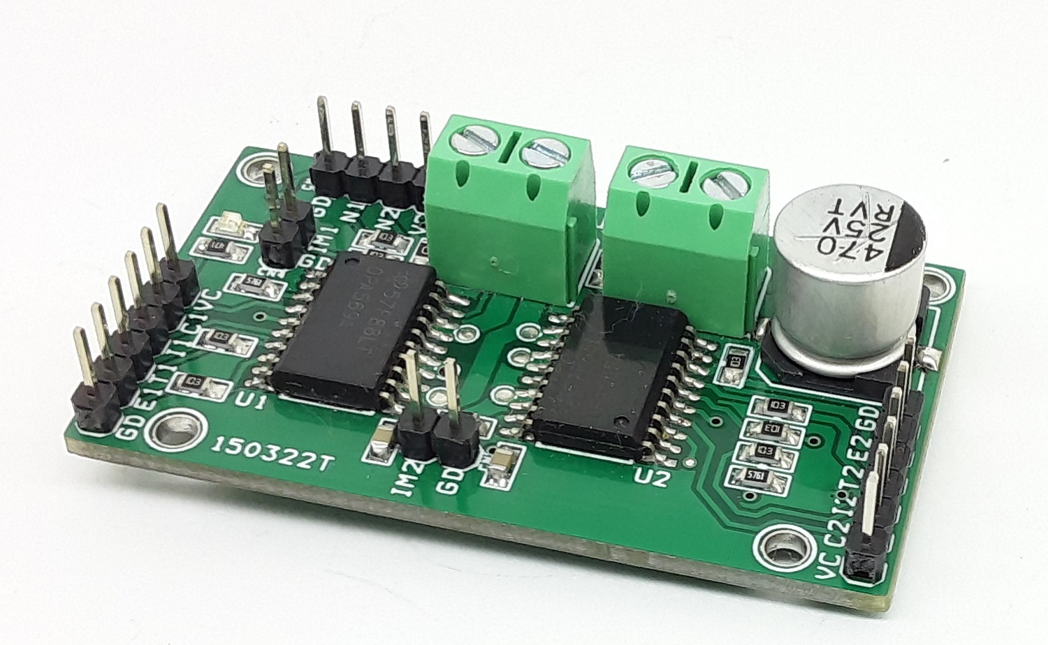
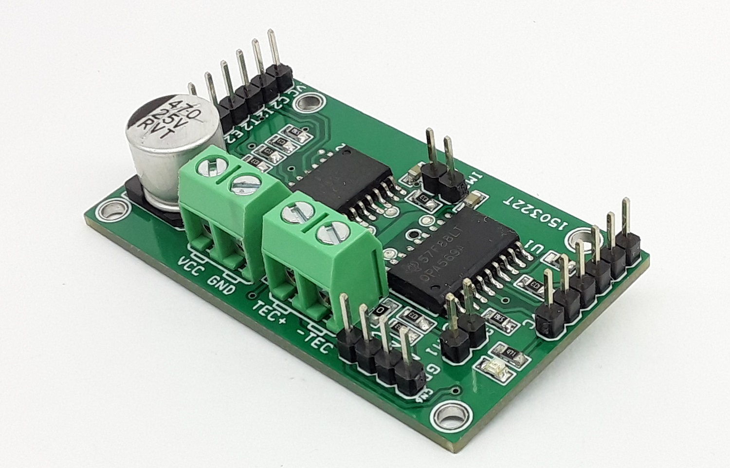
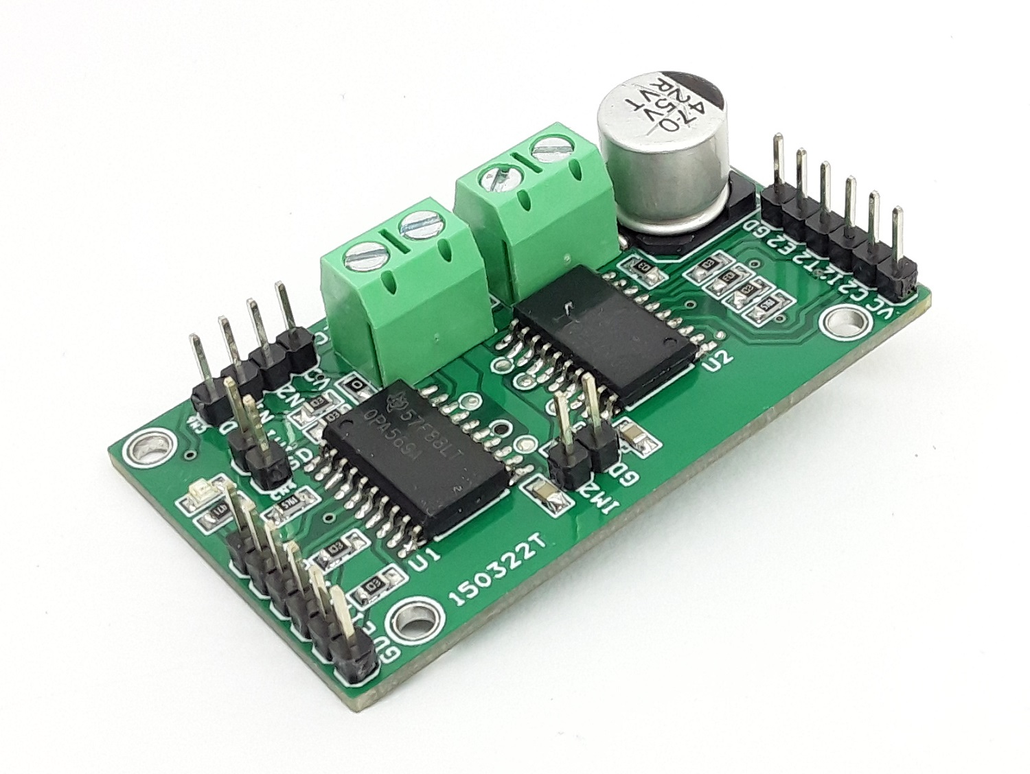
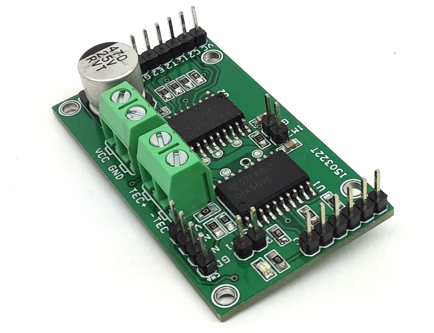
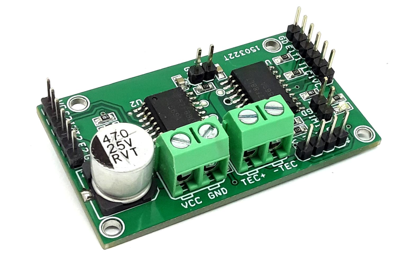
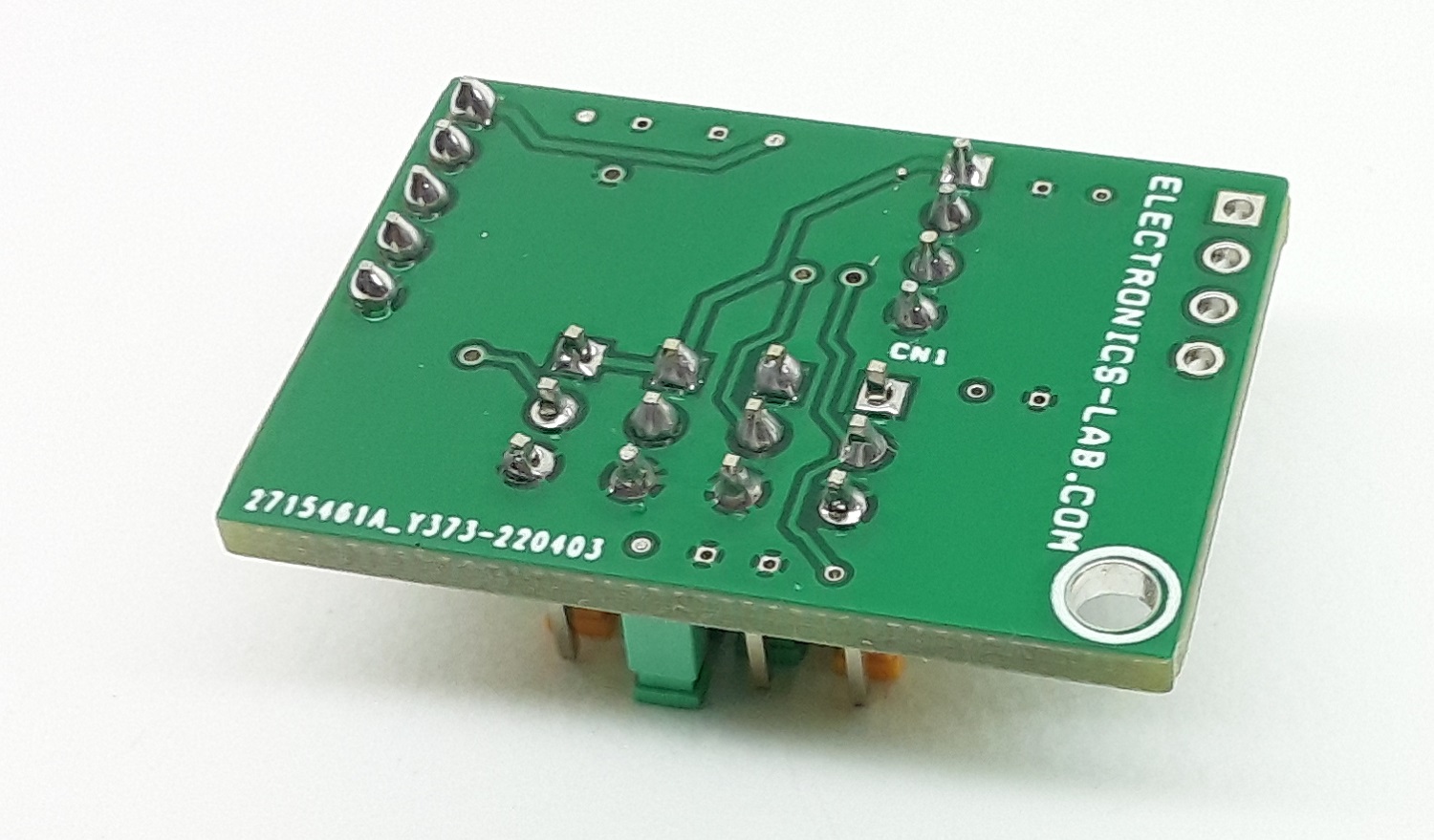
Photos

Video