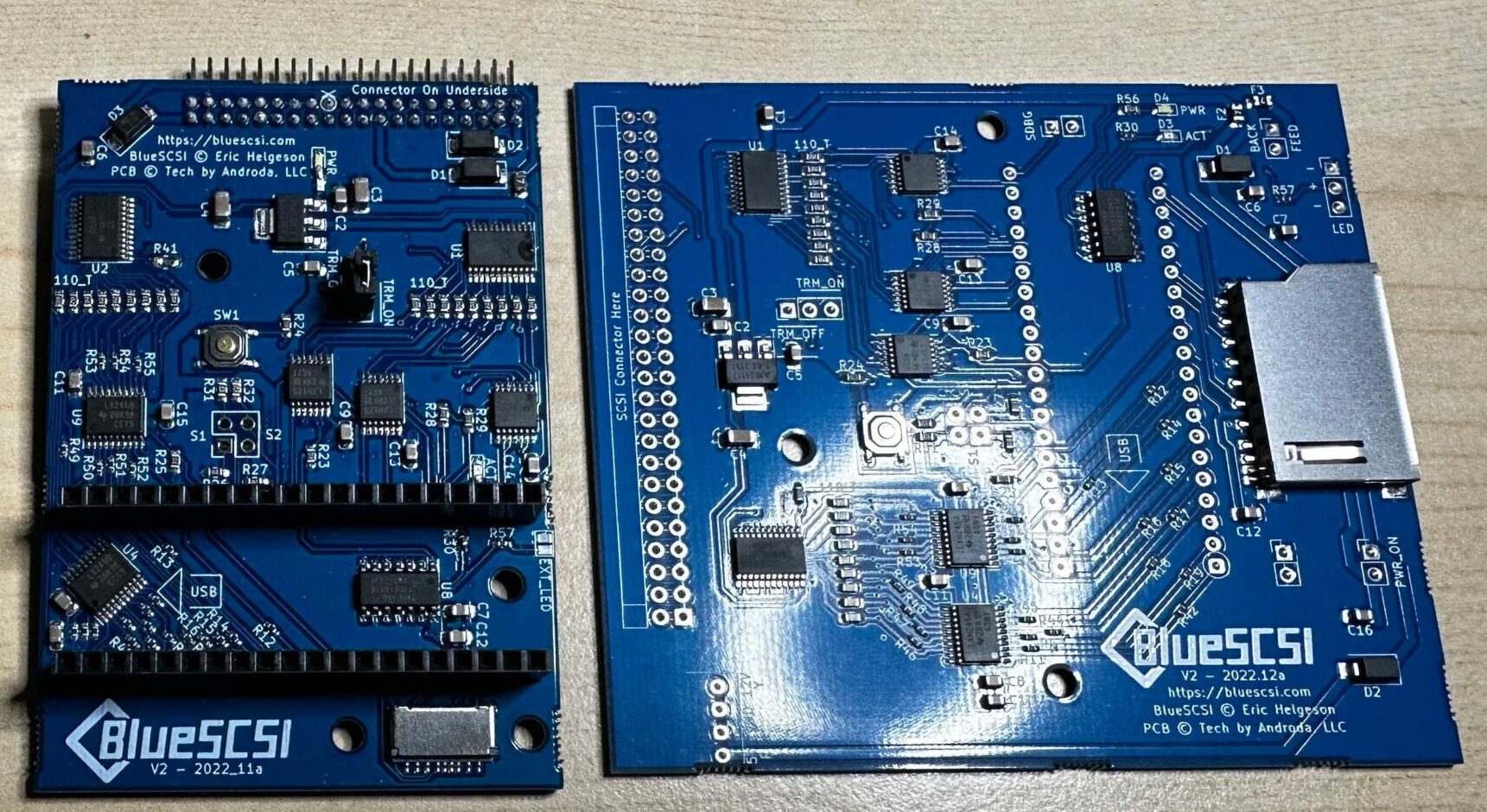
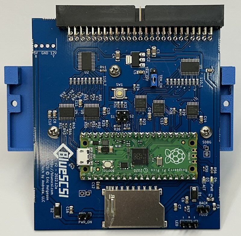
BlueSCSI v2 is back with a second version of their popular SCSI hard drive emulator. The BlueSCSI hardware can reproduce SCSI devices like hard drives, optical drives, SD cards, CD-ROMs, and many more. The product is targeted to provide a reliable and cost-effective solution for vintage computer enthusiasts who are looking to upgrade their old computers. The new version of BlueSCSI is based on raspberry pi pico’s RP2040 microcontroller.
The new BlueSCSI v2 is completely open source, with open hardware and open design. The SCSI2SD firmware is a popular open-source firmware that is used by many SCSI to SD Card adapters. It provides a SCSI interface that allows the adapter to emulate a SCSI device, such as a hard drive or CD-ROM. This allows vintage computers and gaming consoles to access the SD card as if it were a SCSI device. The BlueSCSI v2 adapter uses a modified version of the ZuluSCSI’s SCSI2SD firmware, which has been bifurcated from the original codebase. This means that the BlueSCSI v2 firmware is based on the original SCSI2SD code but has been modified to suit the specific needs of the BlueSCSI v2 adapter. The modified firmware is open-source, which means that it can be modified and improved upon by the community.
One of the benefits of using the Raspberry Pi Pico microcontroller is its flexibility. The microcontroller features a large number of GPIO pins that can be used to interface with a variety of hardware devices, such as SD cards and SCSI interfaces. The Pico also features built-in support for SPI and I2C communication protocols, which are commonly used in SCSI to SD Card adapters.
In the first version of the BlueSCSI a blue pill microcontroller was used, which is now replaced by raspberry pi pico’s RP2040 microcontroller. This results in better performance in terms of processing power, data transfer speed, and future expandability of the device. For comparison, version one on a 10Mbit data bus could transfer 1.3MB/sec, but the new version can transfer 5.8MB/sec on a 5Mbit data bus. It can transfer up to 8.4MB/sec on a 10Mbit bus.
One of the new features of v2 is the SCSI toolbox, and this is an application interface with two major functions. First is that it allows moving files between the host computer and the root of the SD card. This makes file transfer from modern machines a hassle-free process. The second feature is that the new version allows SD hot swapping while powered and attached to the host computer. Some of the advanced features include better human-readable logs, USB serial logging, and onboard LEDs to show the status of the device.
The BlueSCSI v2 retails at the same price as version 1 but gives many new features. To learn more about the emulator, visit the product page.
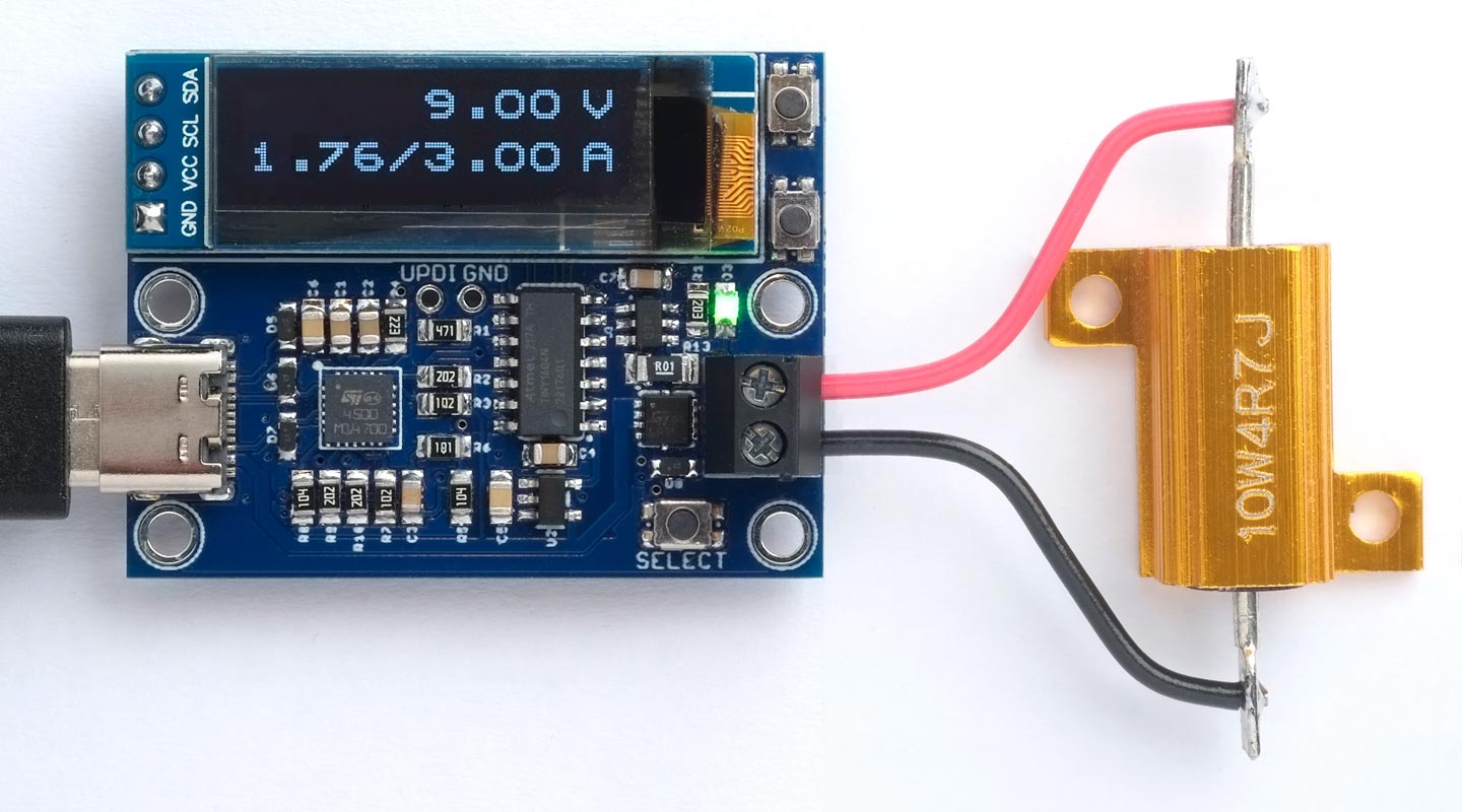
The Power Deliverer utilizes a USB-C power adapter as a power source for a range of fixed voltages. The device displays a list of voltages and current sources from the adapter, which the users can select. Once a voltage option is selected, the Power Deliverer continuously monitors the current usage and presents it on the device’s display. The Power Deliverer is based on STUSB4500, INA181, and ATtiny1604 microcontrollers. The output display used is a 128×32 OLED display which features excellent contrast and brightness.
The current monitor works by measuring the voltage drop across a current sensing resistor, and it is placed between the positive voltage output and the load. It is commonly known as a “high-side” current monitor. However, the positive rail can be as high as 20V. It becomes impractical to directly measure this using an analog input on the microcontroller. Therefore, to measure this voltage drop, two matched high-precision voltage dividers are required, or an alternative option would be to use an analog sensor like the INA181A2.
Working and Circuitry of Power Deliverer
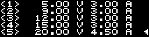
When the user connects the Power Deliverer board to the USB-C charger, it displays a range of voltages and current options available. The device can offer a maximum of 20V at 5A. A green LED also lights up to show that the output is active. If the charger is not supported, the display shows “NO PD” as the output.
The STUSB4500 is a USB power delivery controller and is controlled via the I2C interface by an ATtiny1604 processor. The way the STUSB4500 works is that it allows you to define between one and three Sink PDOs, and it automatically selects the highest-voltage Source PDO available from the charger with the required current capability. Thus STUSB4500 works as a regulator which controls the power supply by allowing the required amount of power. The initial default PDOs are 5V 1.5A, 15V 1.5A, and 20V 1A.
The display used is a 128×32 monochrome OLED display based on the SSD1306 display controller. To fit five power profiles on a 32-bit pixel display, the 5×5 matrix form factor is used. The Power Deliverer is compatible with Apple’s 35W dual power adapter (A2676), Apple’s 96W power adapter (A2166), Apple’s 140W power adapter (A2452), a UGREEN 20W PD Fast Charger with PPS (CD137), and an AUKEY Omnia Mix 3 90W charger (PA-B6S).
For more information on the power deliverer, visit the project page.
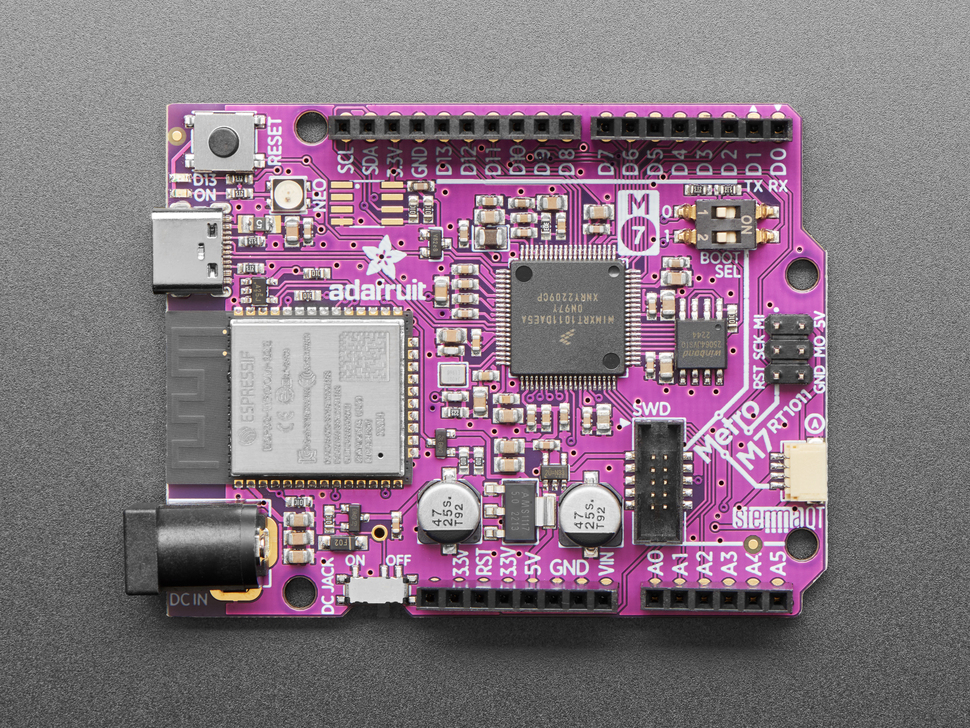
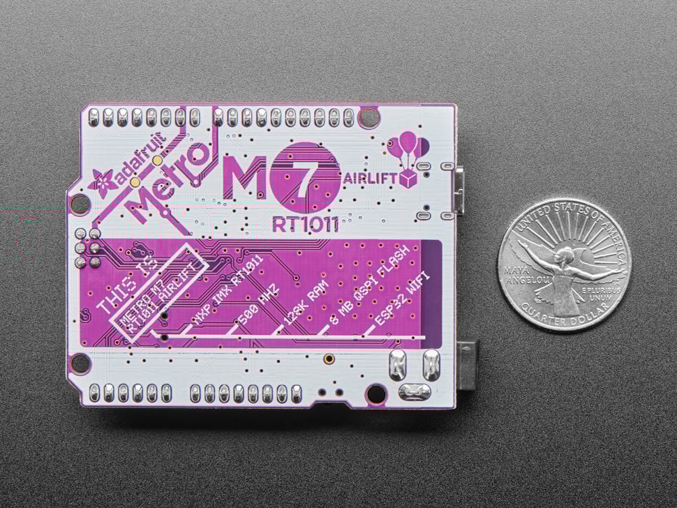
After being teased nearly three years ago, Adafruit finally announced its Arduino Uno-layout Metro M7 development board, based on the NXP i.MX RT1011 “crossover microcontroller unit,” is heading to production. Adafruit first announced the design of the Metro M7 back in 2020, shortly after revealing the Metro ESP32-S2, which is based on Espressif‘s Wi-Fi-capable module of the same name. The Metro ESP32-S2 is now available to purchase for $19.95 before volume discounts, but the Metro M7 has taken longer to reach production.
About the Metro M7, Adafruit says
“We stayed in and worked on the Metro M7 featuring the i.MX RT1011 (the lil’ sister chip to the RT1062 that stars in the Teensy 4)’’. They continue ‘‘This chip is really fast, clocking at 500 MHz, and has 128k of RAM. For flash, it uses an external QSPI chip which we’ll share for filesystem use as well.”
Adafruit’s Metro M7 is a powerful device, featuring NXP’s i.MX RT1011, part of the company’s “crossover microcontroller unit” range. This chip has a single Arm Cortex-M7 core running at 500MHz and 128kB of SRAM, and is paired with an Espressif ESP32-WROOM-32 module as a Wi-Fi coprocessor, a concept Adafruit has dubbed “AirLift.”
On the board, there is 4MB of quad-SPI (QSPI) flash memory with execute-in-place (XIP) support, a USB Type-C port for data and power with a barrel jack for 6-12V DC power, a physical reset button plus boot-mode switches, a Serial Wire Debug (SWD) connector, power switch, and a STEMMA QT connector for external I2C hardware.
Adafruit has created a UF2 bootload for the Metro M7 board to make it easy to install the CircuitPython firmware, making it likely the fastest non-Linux-capable Arduino UNO-compatible board on the market. You don’t need any special DFU/firmware-updater software to use UF2, as it allows you to simply drag-and-drop UF2 files and has a nice LED/NeoPixel indicator. Any computer can be used to program a UF2-bootloader device, and once installed, you can access the UF2 bootloader by double-clicking the reset button. Anyone who has used an Arduino Uno in the past will find the spacing of the pin headers to be immediately familiar, and they should offer at least partial compatibility with Arduino Uno shield accessories.
The Metro M7 board is out of stock at the Adafruit store, where it is sold for $29.99.
If you want to be notified when the board is back in stock, you can leave your email on the Adafruit website. For more information about the Metro M7, visit Adafruit blog.
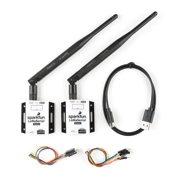
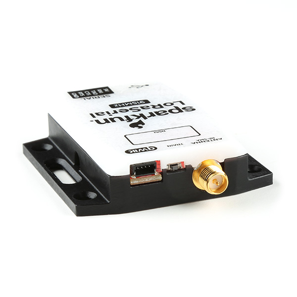
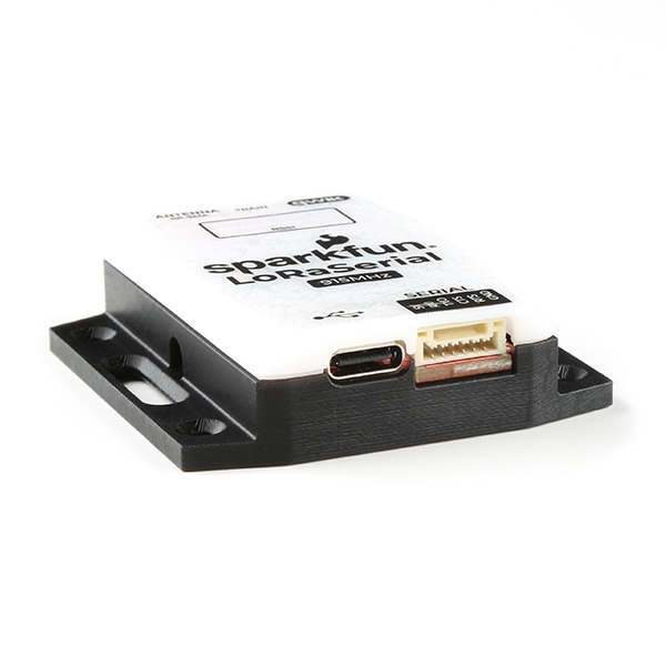
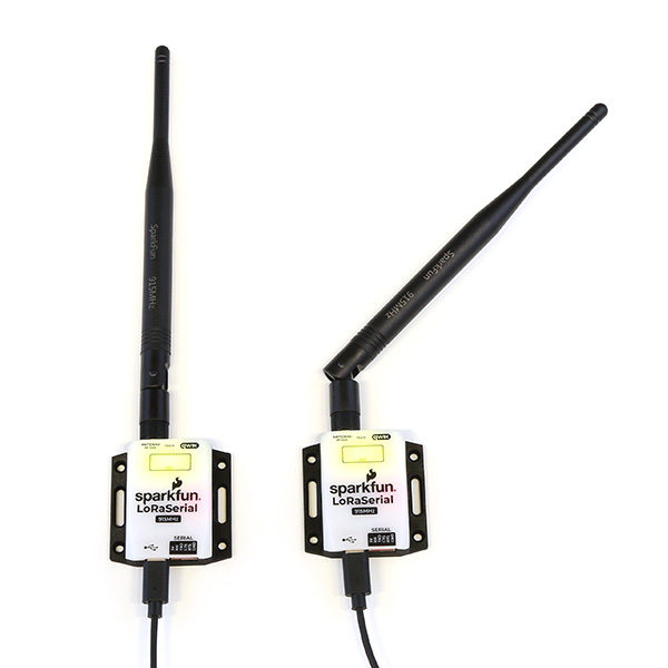
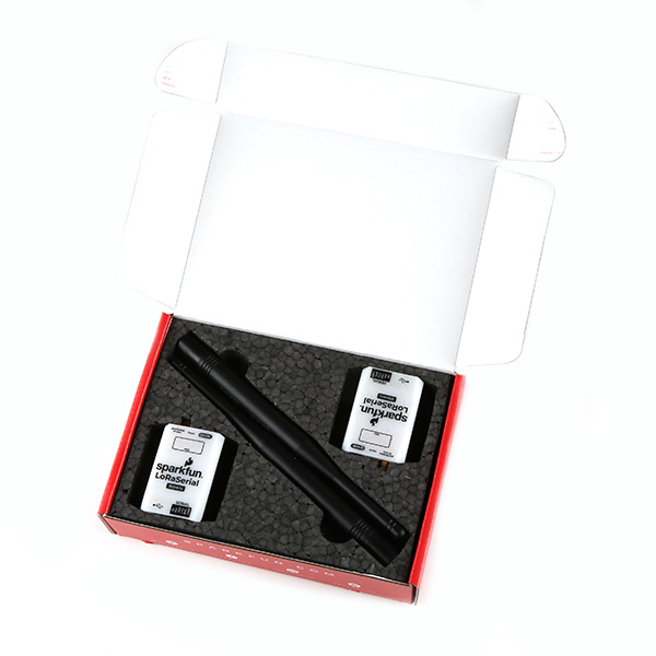
The SparkFun LoRaSerial Kit is a great way to transmit data over LoRa, providing you with a range far greater than that of WiFi or Bluetooth®. We’ve been able to successfully transmit data over a 9mi (15km) line-of-sight using two LoRaSerial radios with a larger 5.8dBi antenna on the transmitter and the stock 1/2 wave dipole antenna on the receiver. This kit is a pair of serial radio modems that simply passes serial back and forth between one another, allowing you to report data every few seconds even if it’s located beyond WiFi or Bluetooth® range.
The SparkFun Kit features a LoRa SX1276-based 915MHz unlicensed band radio with 902-928MHz configurable output, 256-bit AES GCM encryption, AT command set, built-in Frequency Hopping Spread Spectrum (FHSS) technology, point-to-point and multipoint configurations, 3D printed enclosure (may darken over time), configurable air speeds from 400 bps (40 bytes per second) to 19200bps (1920 bytes per second), configurable standard serial data rates from 2400 to 115200bps, 4-LED RSSI indicator, 3.3 to 5V operation, USB-C connection available for industrial systems and single-board computers (SBCs like Raspberry Pi), 6-pin JST connector available for embedded systems (5V and 3.3V tolerant I/O) with flow control, small footprint, lightweight, easily mountable, and open source software and hardware with 1 Watt (30dBm) power output.
This LoRaSerial Kit is perfect for GNSS RTK and many other geospatial scenarios, as it supports both simple point-to-point communication and multipoint broadcasting, allowing one device to produce and disseminate data to multiple other devices. Pressing the train button on both radios with the LoRaSerial firmware will generate a new random network ID and AES encryption key to share, making pairing radios in the field as easy as a single button press. This innovative and straightforward training method ensures that bringing the radios near each other is both secure and simple.
SparkFun is currently offering radios in the LoRaSerial Kit that utilize 915MHz modems, which are allowed in most parts of the world. However, please check your local restrictions before purchasing, as the radios are fully configurable to restrict frequencies, channels, dwell time, power output, and a variety of other settings to make them compatible with your local regulations.
SparkFun states that LoRaSerial is designed to operate at the physical layer of LoRa, sending data directly to an endpoint, rather than on the data and network layers like LoRaWAN. Therefore, LoRaSerial is not intended to be used with LoRaWAN.
For more information about the LoRaSerial Kit and documentation, visit the product page.
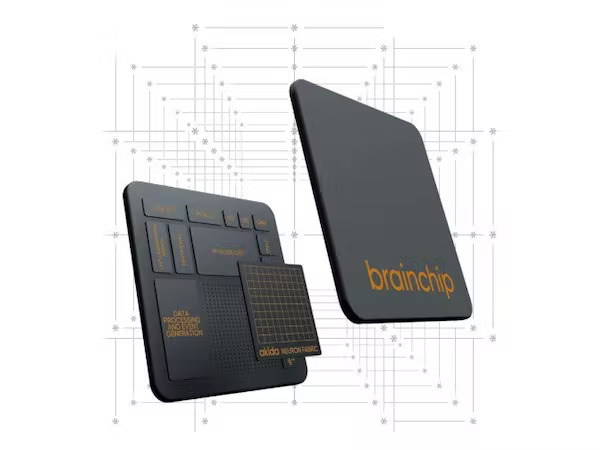
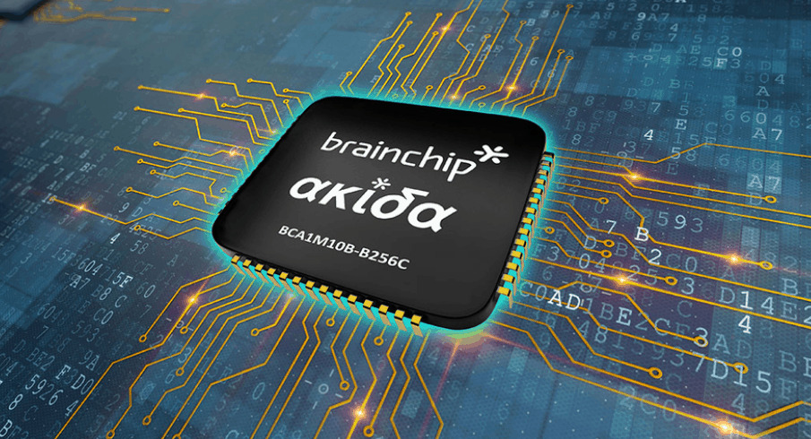
BrainChip has unveiled the second generation of its Akida platform, designed for energy-efficient and intelligent edge devices for the rapidly growing demand for artificial intelligence in the IoT ecosystem. The new Akida platform features a neural processing system designed for embedded edge AI applications, featuring 8-bit processing and advanced capabilities such as time domain convolutions and vision transformer acceleration. This enables the device to deliver high performance in sub-watt devices, moving from perception to cognition.
The key highlight of the Akida is the Temporal Event-based Neural Nets (TENN) spatial-temporal convolutions that enable the processing of raw time-continuous streaming data such as video analytics, target tracking, and audio classification. At the same time, time series analytics is used in forecasting and predictive maintenance. These capabilities are important for application in industrial, automotive, digital health, smart home, and smart city industries.
Temporal Event-based Neural Nets are a type of neural network that can handle temporal data which changes over time. They process this data only when there is a change in the input stream, inspired by how the human brain processes sensory data. The spatial temporal convolutions are used to extract features from the input data relevant to the task. Combining these two allows the Akida platform to perform complex tasks with low power consumption.
“We see an increasing demand for real-time, on-device intelligence in AI applications powered by our MCUs and the need to make sensors smarter for industrial and IoT devices,” said Roger Wendelken, Senior Vice President in Renesas’ IoT and Infrastructure Business Unit. “We licensed Akida neural processors because of their unique neuromorphic approach to bring hyper-efficient acceleration for today’s mainstream AI models at the edge.
Another upgrade to the Akida platform is the addition of Vision Transformers (ViT) acceleration. This edge neural network has been used to process data in various computer vision tasks such as image classification, object detection, and semantic segmentation. This acceleration mechanism, when combined with Akida’s ability to process multiple layers simultaneously, allows it to self-manage the execution of complex networks like RESNET-50.
The device combines efficiency and performance to enable very differentiated solutions that include secure, small form factor devices like hearable and wearable devices and medical devices for monitoring the heart that consumes only microwatts of power. According to the press release, the platform will be publicly available in Q3 of 2023.
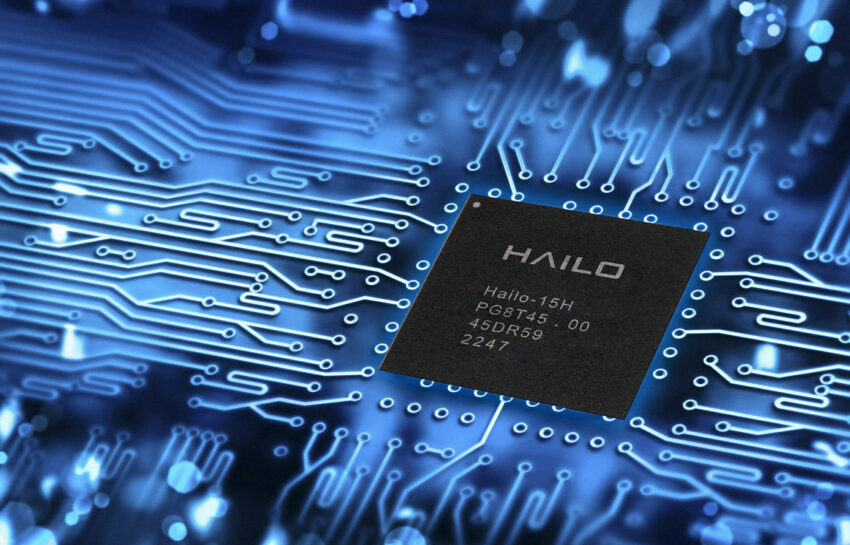
Hailo has introduced the Hailo-15 series of advanced vision processors, which are specifically created to be incorporated into smart cameras. The Hailo-15 lineup raises the benchmark for computer vision and video processing using deep learning, offering exceptional AI capabilities for a range of applications in diverse industries.
Hailo has introduced a family of VPU (Vision Processing Unit) consisting of three models: Hailo-15H, Hailo-15M, and Hailo-15L. Each of these variants is designed to cater to different processing requirements and budgets of smart camera manufacturers and AI application providers. The Hailo-15 series can significantly improve the efficiency and accuracy of various industries such as smart cities, manufacturing, and retail, enabling them to detect incidents quickly, increase productivity, reduce downtime, and enhance customer satisfaction.
“Hailo-15 represents a significant step forward in making AI at the edge more scalable and affordable,” stated Orr Danon, CEO of Hailo. “With this launch, we are leveraging our leadership in edge solutions, which are already deployed by hundreds of customers worldwide; the maturity of our AI technology; and our comprehensive software suite, to enable high performance AI in a camera form-factor.”
The Hailo-15 AI vision processor enables the Hailo-15 camera development kit to offer exceptional AI analytics and superior image quality. This development kit provides all the necessary components for creating and testing a camera prototype that meets the increasing demand for advanced video processing and analytics at the edge of the network. Hailo is responding to this trend by incorporating cutting-edge AI capabilities directly into the camera.
Previously, the company had launched a Hailo-8 processor for edge AI, which had the capacity to perform up to 26 tera-operations per second (TOPS), surpassing all other edge processors by a significant margin. The Hailo-8 neural chip utilizes neural network core properties, enabling edge devices to run deep learning applications more efficiently, effectively, and sustainably than other AI chips and solutions. Additionally, the Hailo-8 chip reduces costs considerably.
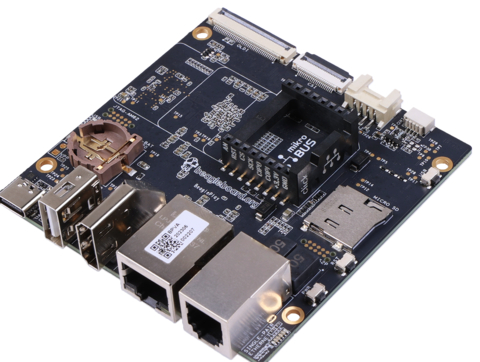
The BeagleBoard Foundation has released BeaglePlay, an open-source performance platform that provides a flexible solution for users with varying levels of experience. With its wide range of connectivity options, BeaglePlay allows users to connect with numerous sensor and prototyping systems, making it an incredibly versatile tool for developers.
BeaglePlay utilizes an open-source Linux approach based on the Texas Instruments AM625 processor that features four 64-bit Arm Cortex-A53 processor cores and low-latency microcontroller subsystems. The processor also includes a dedicated Texas Instruments SimpleLink CC1352P7 sub-1 GHz and 2.4-GHz wireless microcontroller and a Texas Instruments WiLink WL1807MOD Wi-Fi module.
BeaglePlaycomes with a tailored Debian Linux image from the BeagleBoard Foundation that includes a pre-installed desktop and features such as a Wi-Fi access point and BeagleConnect gateway functionality allowing rapid and flexible development options. Additionally, the software supports several application libraries and examples from Linux, Zephyr, MicroPython, and other open-source frameworks, making it effortless for users to incorporate various features into their projects.
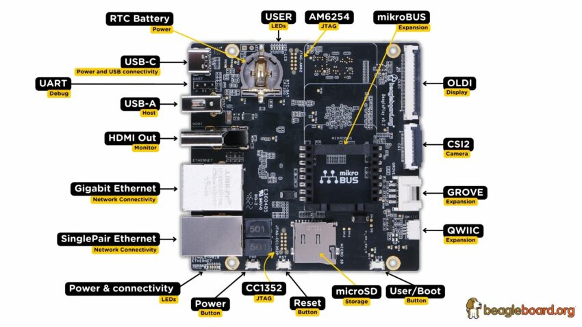
Specifications of BeaglePlay hardware device
Processor: Texas Instruments AM62x Sitara processor series– TI AM6254 multicore A53 with R5, M4s and PRUs
Integrated power management: TPS6521901
Memory: 2GB DDR4 memory
Storage: 16GB eMMC and microSD card slot
Wireless connectivity: WL1807MOD module for 2.4GHz and 5GHz dual-band Wi-Fi and CC1352P7 for Bluetooth Low Energy
Interfaces: USB Type-C, HDMI port, mikroBUS connector, Grove, QWIIC, CSI connector, and an OLDI connector
Furthermore, BeagleConnect technology allows users to connect to remote sensors up to a distance of 1km away, using the sub-1GHz IEEE 802.15.4 wireless network to a BeagleConnect Freedom, which is particularly beneficial for remote sensing applications. This feature significantly enhances the flexibility of the BeaglePlay platform.
The Texas Instruments AM625 application processors are intended for developing Linux applications and are equipped with embedded features such as 3D graphics acceleration and dual-display support. These processors are available in two sizes: an industrial-grade 13×13 mm package (ALW) and a 17.2×17.2 mm package (AMC), which meets the AEC-Q100 automotive standard.
The processors have integrated Cortex-M4F cores and specialized peripherals, which can be separated from the rest of the AM62x processor to meet functional safety requirements for industrial and automotive applications. The board is currently listed on Element 14 for $108.90.
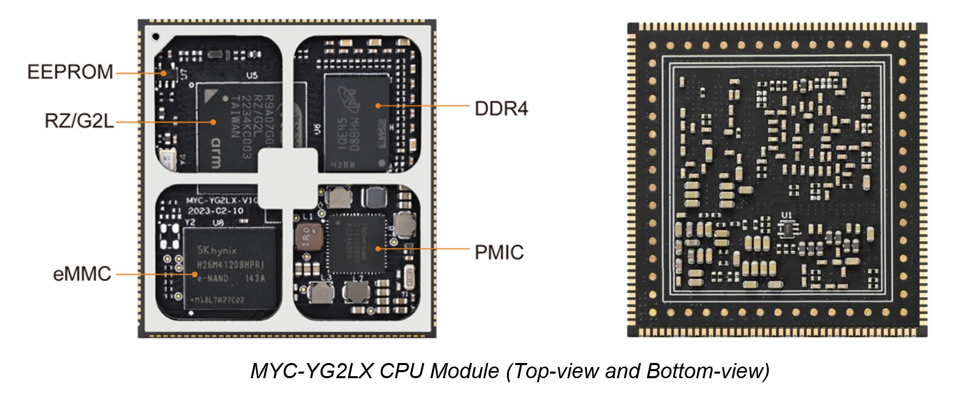
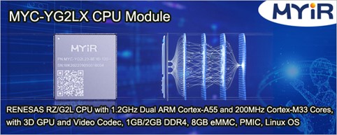
MYIR has launched MYC-YG2LX CPU Module based on RENESAS RZ/G2L SoC which features 1.2GHz dual ARM Cortex-A55 and 200MHz Cortex-M33 cores with high-performance Mali-G31 GPU and built-in video codec engine as well as various peripheral interfaces such as camera input, display output, USB 2.0, and GigE-Ether. In addition to the SoC, the MYC-YG2LX has integrated 1GB/2GB DDR4, 8GB eMMC, 32Kbit EEPROM and PMIC. A variety of peripheral and IO signals are accessible via the 1.0 mm pitch 222-pin Castellated-Hole expansion interface. It provides a cost-effective SoM solution for advanced HMI, IoT Edge Computing Gateway and embedded devices with video capabilities.
The MYC-YG2LX CPU Module has a small form factor, measuring only 45mm by 43mm. It is ready to run Linux OS and provided with image files, kernel and driver source codes, application demos and compilation tools to enable users to start their development rapidly and easily.
Features Of MYC-YG2LX CPU Module
Dimensions: 45mm x 43mm
PCB Layers: 10-layer design
Power supply: 5V/1A
Working temperature: -40~85 Celsius (industrial grade)
RENESAS RZ/G2L processor (R9A07G044L23GBG)
1G/2G DDR4 (supports optional 4GB)
8GB eMMC (supports optional 4GB, 16GB / 32GB)
32KB EEPROM
Power Management IC (RAA215300)
0mm pitch 222-pin stamp hole expansion interface
– 2 x RGMII
– 4 x I2C
– 3 x SPI
– 2 x USB 2.0
– 1 x MIPI DSI
– 1 x MIPI CSI
– 1 x Parallel CSI
– 1 x RGB
– 2 x SCI
– 5 x SCIF
– 8 x ADC
– 4 x SSI
– 1 x SRC
– 2 x CAN
– Up to 118 GPIOs
Note: the peripheral signals brought out to the expansion interface are listed in maximum number. Some signals are reused. Please refer to the processor datasheet and CPU Module pin-out description file.
Linux OS
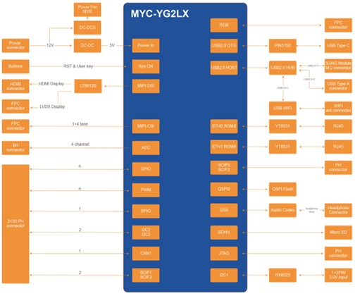
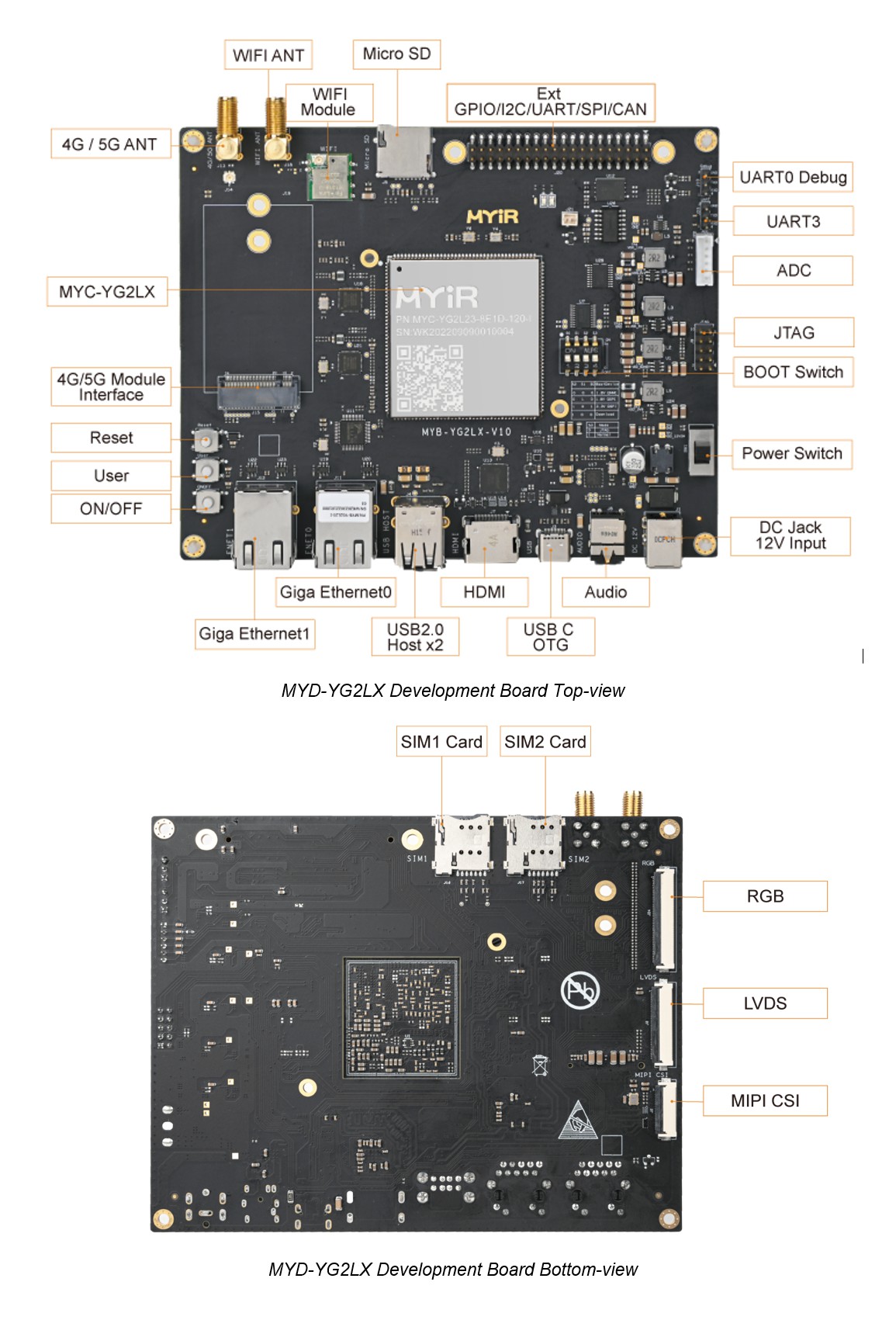
MYIR has designed a versatile development board MYD-YG2LX, using the MYC-YG2LX CPU Module as core controller module. It is a complete evaluation platform and has provided an ideal base board prototype reference design for using the MYC-YG2LX. A plenty of peripherals interfaces are carried out to the base board through the 1.0 mm pitch 222-pin Castellated-Hole expansion interface including Serial ports, two Gigabit Ethernet, two USB 2.0 HOST and one USB 2.0 OTG, one Micro SD card slot, one M.2 Socket for USB based 4G/5G LTE Module with two SIM card holders, one USB2.0 based WiFi module, one GPIO/I2C/UART/SPI/CAN extension header, Audio input/output, MIPI-CSI camera interface as well as HDMI, LVDS and RGB video output interfaces, etc. MYIR also offers camera modules, RPI COM Module (RS232/RS485/CAN) and LCD modules as add-on options to work with the board for further enhancing the functionality of the board.
MYD-YG2LX Development Board Function Block Diagram
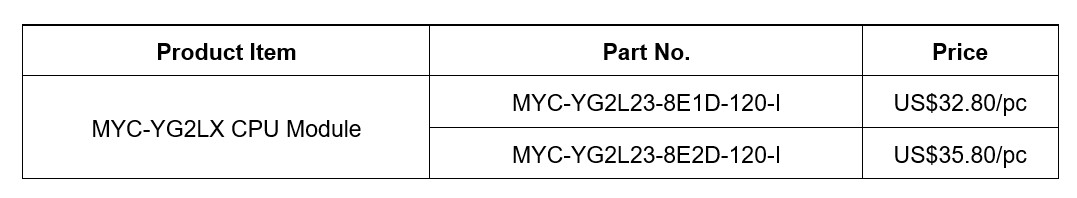
MYIR offers 1GB and 2GB DDR4 version options for the MYC-YG2LX CPU Module. The prices are economic but the module has high performance and reliable quality. Discount is to be offered for volume quantities. MYIR also provides OEM/ODM services to help customers accelerate their time to market and save costs.
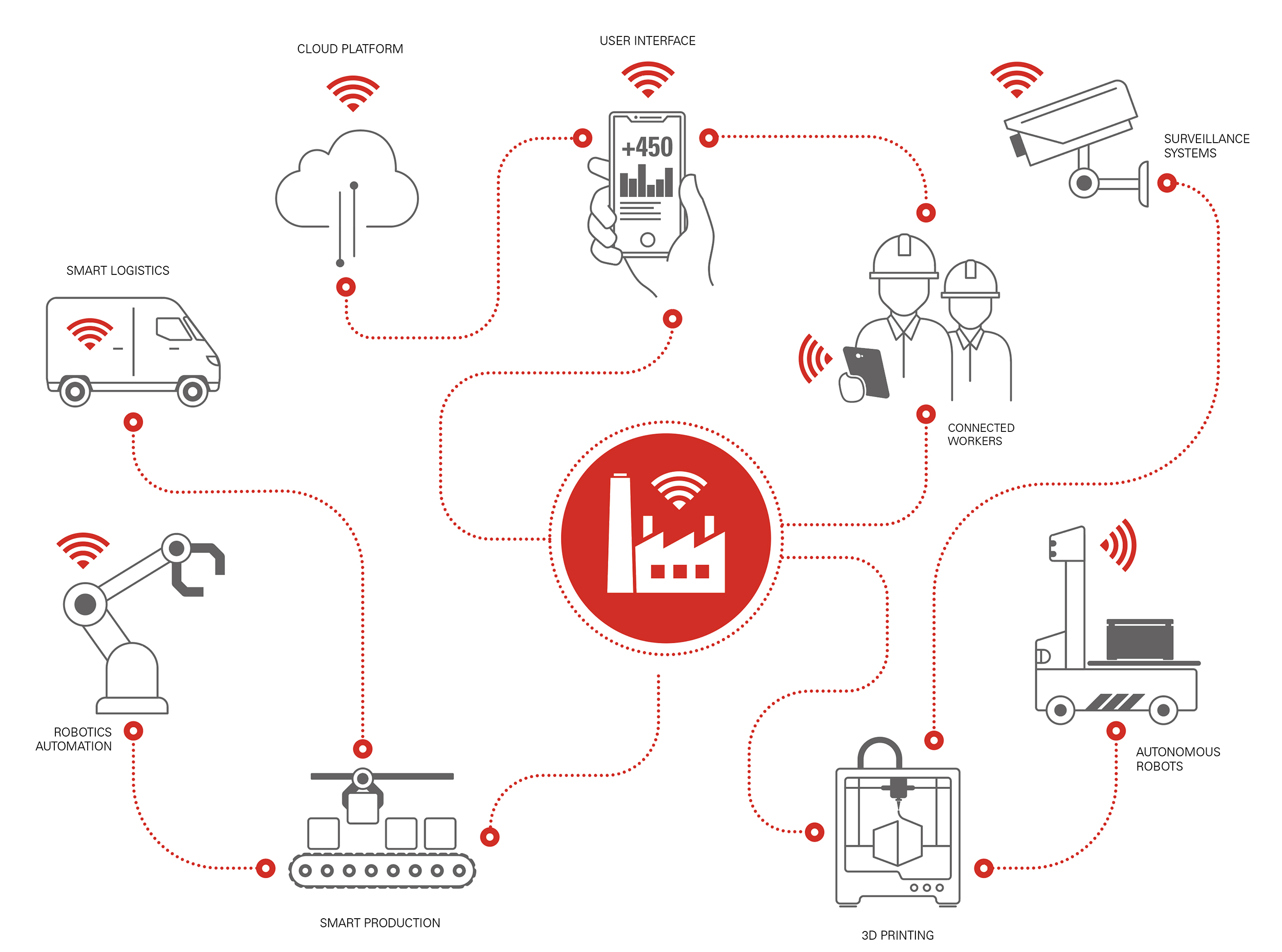
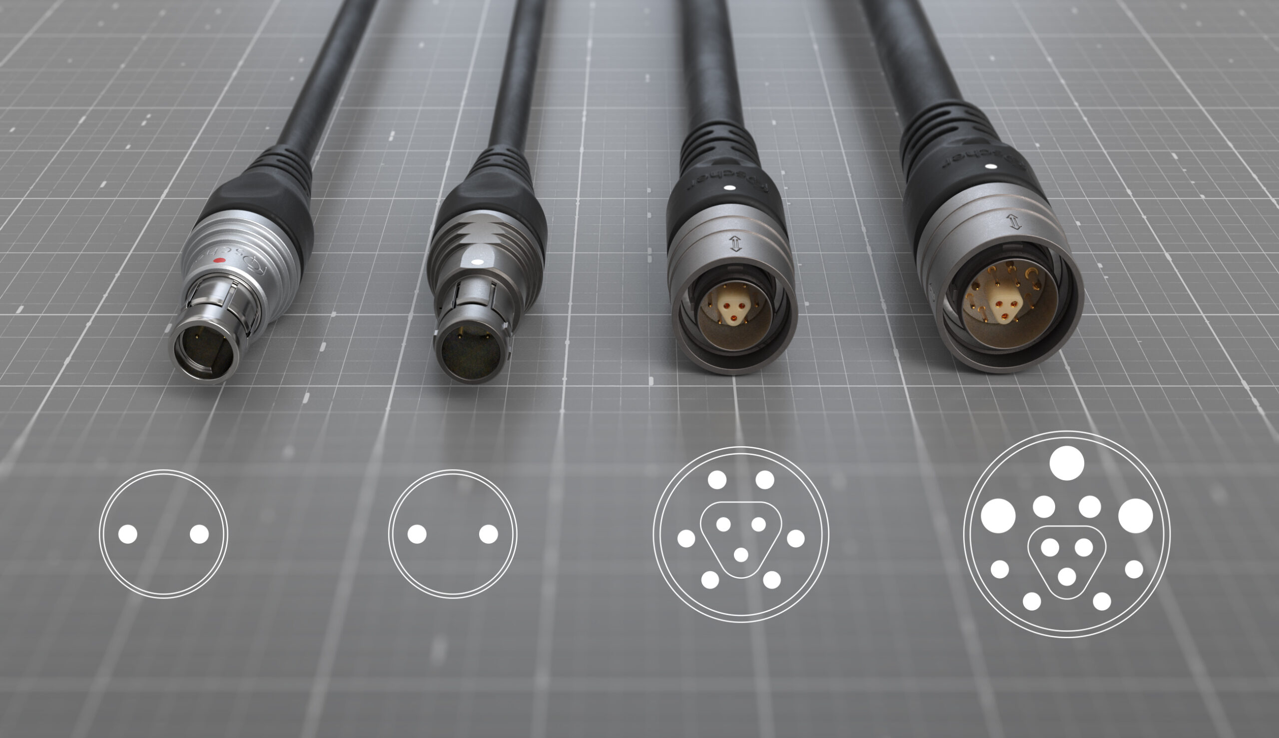
Fischer Connectors, the Swiss-based global leader in high-performance connectivity, releases ultra-robust Single Pair Ethernet (SPE) and USB 3.2 Gen 2 connectivity solutions to meet the specific requirements of Industrial Internet of Things (IIoT) applications in rugged environments.
With the increase in sensor density, actuators and controllers in Industry 4.0 and IIoT operational settings, high power levels and massive amounts of data must be securely and efficiently managed through ultra-fast transmission lines with cables running over long distances. Miniature connectors and cables are needed to interconnect smaller and smaller devices and sensors in areas that are sometimes confined and hard to access. And connectivity must be ruggedized to resist shock, vibration, extreme temperatures, water and corrosion when exposed to demanding environmental and chemical conditions, both indoors and outdoors.
To address these challenges, Fischer Connectors has developed new high-speed data and power connectivity solutions combining Single Pair Ethernet and USB 3.2 Gen 2 high-speed protocols with the rugged, high-density and miniature features of its flagship product lines. They enable space-saving and cost-efficient integration in industrial automation and robotics, chemical plants, food processing, automotive production lines, outdoor sensing and unmanned systems.
The Single Pair Ethernet solutions from the Fischer Core Series and Fischer UltiMate™ Series allow for 1 Gbit/s data transfer per IEEE 802.3bp – 1000Base-T1. Exceptionally rugged by any market standards, they outperform other suppliers’ SPE solutions in terms of security, durability, as well as environmental and mechanical performance. Fischer SPE is compliant with MIL-STD norms (through Fischer UltiMate™) and offers 10,000 mating cycles, three locking mechanisms (push-pull, screw, quick-release), and hermetic sealing in addition to IP68/ IP69 ratings. SPE is also featured in the ultra-miniature Fischer MiniMax™ connector in ‘size 06’ (Ø 10 mm receptacle).
The demand for USB 3.0+ protocol is high in Industry 4.0 operations, as it offers high data transfer rates with low latency for IIoT control applications, nearly twice the power output than USB 2.0 (900 mA vs. 500 mA), better power efficiency due to lower consumption in idle state, and larger bandwidth. Fischer MiniMax™ connectors with USB 3.2 Gen 2 allow for 10 Gbit/s data transfer, offer additional power contacts up to 8 A, and are half the size of some competitor connectors with similar speed but no power.
To accompany its product release, Fischer Connectors has published a trend paper entitled “The Connectivity Challenge – Connecting Industry 4.0”. It describes three challenges facing OEM engineers designing IIoT applications, as well as three innovation practices addressing cybersecurity, global logistics and Edge/Cloud infrastructure.
The innovation-driven IIoT market is growing exponentially. With billions of smart sensors, computers and machines connected and operating across the Internet, experts expect an annual increase of over 20%, reaching 1.5 trillion euros by 2030.
A Display Decoder is a type of Binary Decoder, discussed in the previous article, with the main purpose to drive a display. As such, it is a combinational logic circuit that converts input binary data into a corresponding number of output lines which are connected to a display for displaying information such as decimal or hexadecimal numbers.
The Binary or Digital Decoder converts one form of binary data into another defined by its logical functions and is commercially available in the form of an IC package. The most commonly known Digital Decoder is a Binary Coded Decimal (BCD) to 7-Segment Display Decoder which is used to display decimal & hexadecimal numbers from the BCD number. The 7-segment display, as the name says, is divided into seven (7) segments and each segment is made of a Light Emitting Diode (LED) which can be independently turned ON or OFF. The combination of lit segments makes up a decimal number from “0” to “9” or a hexadecimal number from “A” to “F”. For example, commercially available TTL Package 74LS47 is BCD to 7-segment Decoder IC.
7-Segment Display
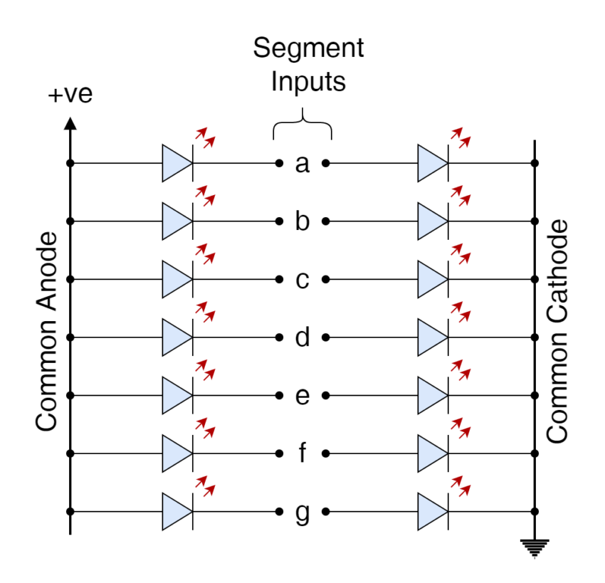
The common LED has two terminals i.e. Anode & Cathode and, as such, each segment (LED) of a 7-segment display has two terminals. In order to reduce wires one of the terminals is kept common and the rest of the wires are used to control the specific segment. This makes a total of eight (8) input connections amongst which seven (7) are for controlling & one (1) is a common line connected to the either positive or negative terminal of the power source. In most of the 7-segment displays, additional input is present to display Decimal Point (DP). Depending on the common terminal, a 7-segment display can be classified into the following categories:
Common Anode Display
In this type of 7-segment display, the anodes of all seven (7) segments are connected together and are connected to logic “HIGH” or positive power terminal. Each segment is then illuminated by connecting its Cathode terminal to logic “LOW” or ground.
Common Cathode Display
In this type of 7-segment display, the cathodes of all seven (7) segments are connected together and are connected to logic “LOW” or ground terminal. Each segment is then illuminated by connecting its Anode terminal to logic “LOW” or ground.
Figure 1: Common Anode and cathode 7-segment display
The above-mentioned configurations either common anode or cathode can be used to display decimal and hexadecimal values on a 7-segment display.
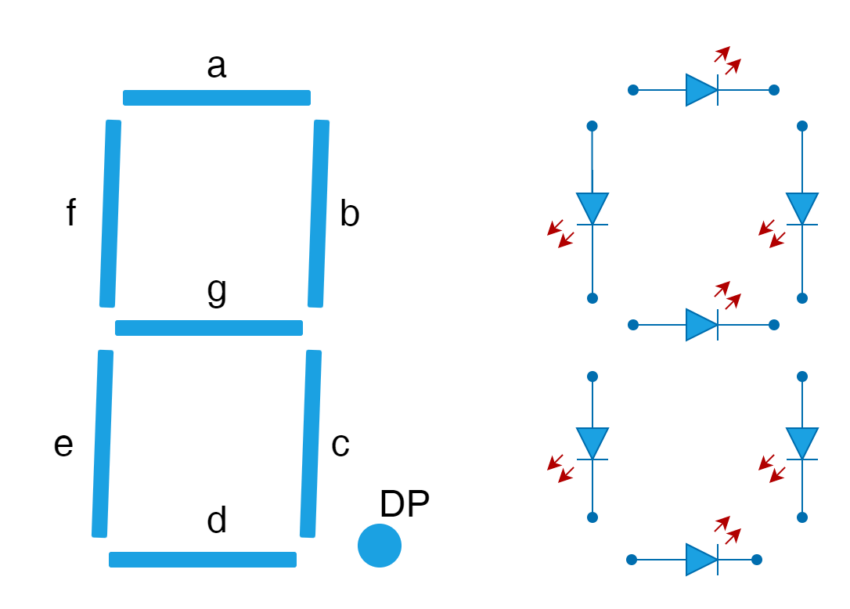
Format of 7-Segment Display
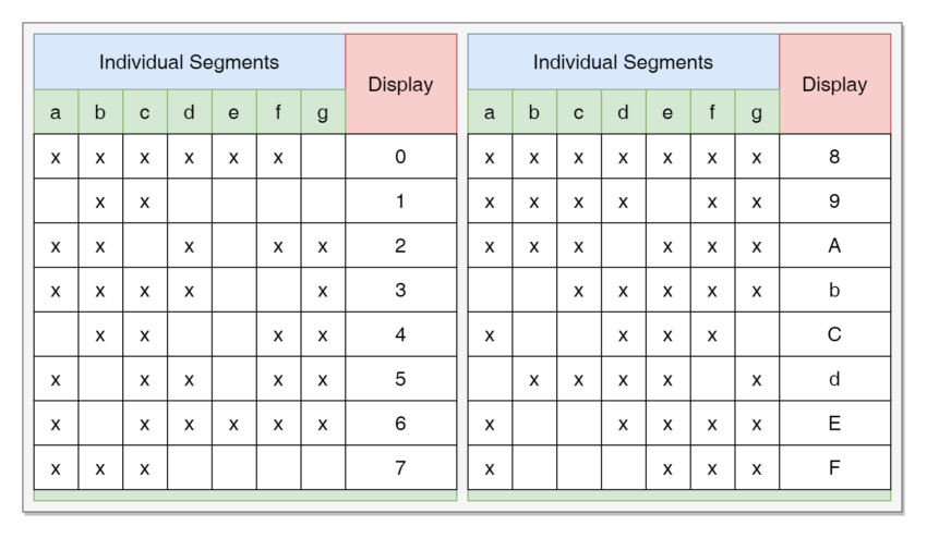
In the following figure, the format of a 7-segment display is showing placement of each segment. The segments are designated as “a”, “b”, “c”, “d”, “e”, “f”, and “g”. In order to display the digit “1” on it, segments “b” & “c” will be illuminated only. Similarly, for displaying digit “7”, segments “a”, “b”, & “c” will be illuminated, accordingly. The same pattern will be followed to display other numeric and alphabetic values and a truth table can be produced illustrating the combination of illuminated segments required for displaying alphanumeric values.
Figure 2: 7-segment display format
7-Segment Truth Table
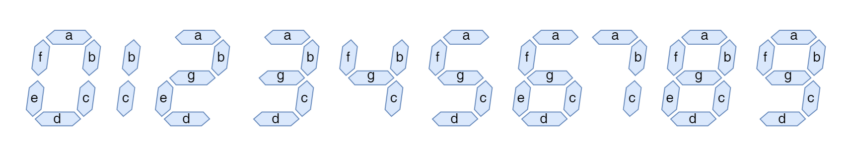
Figure 3: 7-Segment Truth TableFigure 4: Numbers using 7-Segment display
It is eminent from the above Truth Table that a total of eight (8) input connections are required for displaying binary values into 0 to 9 or alphabets from A to F. As each segment consists of a LED which typically takes around 20mA of current when illuminated. So, displaying digit “1” requires illumination of two segments i.e. “b” & “c”, and the total amperage of (2X20mA) is 120mA. Under the illumination of all segments for displaying digit “8” a total amperage of (2X20mA) 140mA is required. Utilization of a number of Inputs/ Outputs (IO) and supplying excessive amperage from a low-cost/ low-powered microcontroller is not feasible. The reduction in number of IOs can be reduced by driving display through a BCD to a 7-segment decoder and displaying on more than one display can be established by multiplexing technique in the microcontroller.
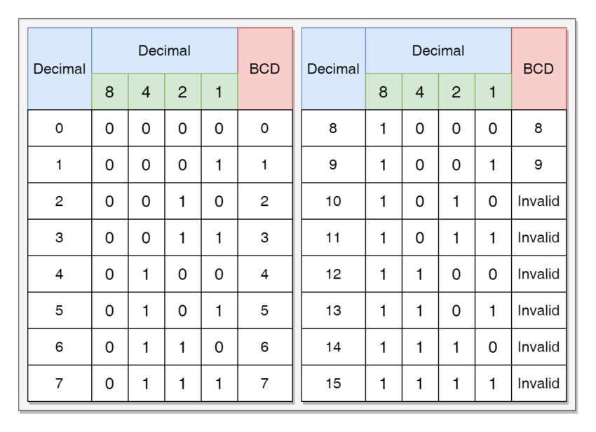
Binary Coded Decimal (BCD)
The Binary Coded Decimal or BCD is a 4-bit binary code to represent a numeric digit. The BCD is also termed as the “8421” code where 8, 4, 2, or 1 corresponds to 2 raised to the power of 3, 2, 1, or 0, respectively. The 4-bit or nibble (half-byte) is used to code a decimal value from 0 to 9 or hexadecimal from 0 to F. However, BCD represents only decimal values from 0 to 9, and the rest of the values from A to F are not used which resultantly produces invalid input for these A to F inputs. The Binary pattern for these BCD numbers is shown in the following truth table.
Figure 5: BCD Truth Table
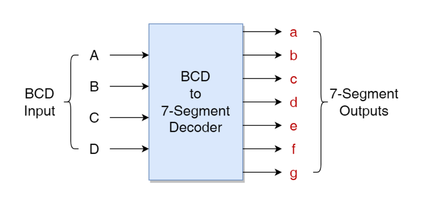
BCD to 7-Segment Display Decoders
As discussed earlier, a Display Decoder is preferred for displaying numbers on a 7-segment display when using a microcontroller due to its limited number of input and output lines as well as less power handling capability. The commercially available BCD to 7-segment Decoders such as TTL 74LS47 or 74LS48 is used for this purpose and has four (4) binary inputs & seven (7) output lines to drive each corresponding 7-segment. These decoders can run a 7-segment display displaying values from 0 to 9 and, similarly, another similar setup can be used to display numbers from 00 to 99 using an eight-bit (8-bit) or a byte of binary data and is termed as packed BCD (8-bit).
Figure 6: Block Diagram of BCD to 7-Segment Decoder
Commercially Available Display Decoders
LED Type
Common Anode: TTL 74LS47
Common Cathode: TTL74LS48
LCD Type
CMOS CD4543
LED or 7-segment displays require a current limiting resistor in each segment and its value is dependent on the LED type. LCD-type displays use less power compared to their counterpart LED displays and are preferred.
Examples of Display Decoder
A number of BCD to 7-segment Decoder examples are given below to illustrate its operation.
Example No. 1
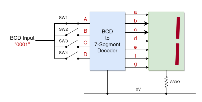
In the following example, the number 1 (one) is displayed on the 7-segment. The corresponding BCD number for one (1) is “0001” as given in the above table. The BCD to 7-segment Decoder decodes this BCD to illuminate corresponding segments by setting logic “HIGH” or “LOW”, depending on the Common Cathode Anode configuration of 7-segment, on its “b”, & “c” output lines.
Figure 7: BCD to 7-Segment Example No. 1
Example No. 2
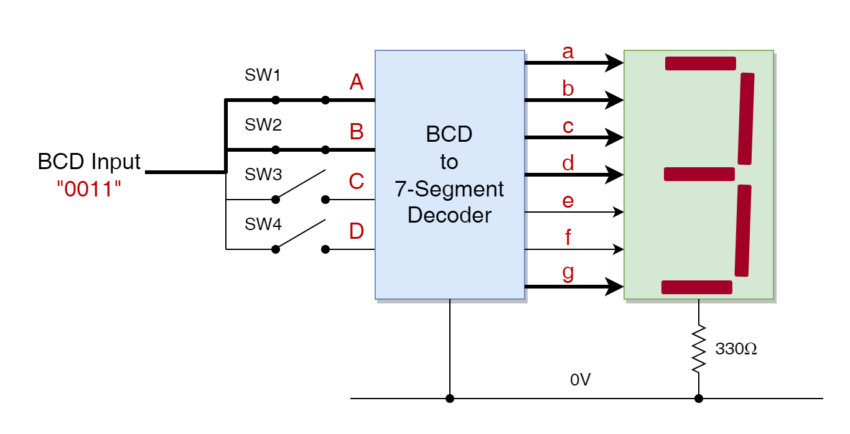
In the following example, the number 3 (three) is displayed on the 7-segment. The corresponding BCD number for three (3) is “0011” as given in the above table. The BCD to 7-segment Decoder decodes this BCD to illuminate corresponding segments by setting logic “HIGH” or “LOW”, depending on the Common Cathode Anode configuration of 7-segment, on its “a”, “b”, “c”, “d”, & “g” output lines.
Figure 8: BCD to 7-Segment Example No. 2
Example No. 3
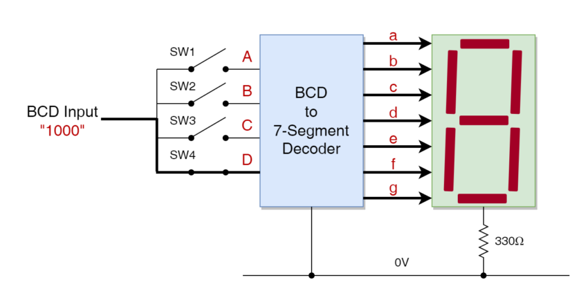
In the following example, the number 8 (eight) is displayed on the 7-segment. The corresponding BCD number for eight (3) is “1000” as given in the above table. The BCD to 7-segment Decoder decodes this BCD to illuminate corresponding segments by setting logic “HIGH” or “LOW”, depending on the Common Cathode Anode configuration of 7-segment, on its “a”, “b”, “c”, “d”, ‘e”, “f” & “g” output lines.
Figure 9: BCD to 7-Segment Example No. 3
Conclusion
A Digital Decoder is a combinational logic circuit that converts n-bit binary code into a number of output lines.
A Display Decoder is a digital decoder used for driving displays for representing binary or binary-coded information.
A 7-segment display comprises seven (7) Light Emitting Diodes (LED) which are enlightened in a combination to display numeric values ad these segments are termed “a”, “b”, “c”, “d”, “e”, “f”, & “g”.
The 7-segment display comes in either a common anode or a common cathode configuration wherein the anodes or cathodes of each segment are joined together, respectively.
The 7-segment display has a total of eight (8) input lines and requires 140mA of current for its seven (7) LED segments. The increased number of input lines and significant amperage makes it impractical to be used with a microcontroller having limited I/O lines and reduced power handling capacity.
A Binary Coded Decimal (BCD) is a 4-bit (nibble) code used for displaying denary numbers from 0 to 9 only. A BCD to 7-segment Decoder is used with a microcontroller to drive a 7-segment display.
Commercially available BCD to 7-segment Decoders are TTL 74LS47 or 74LS48 IC Packages.