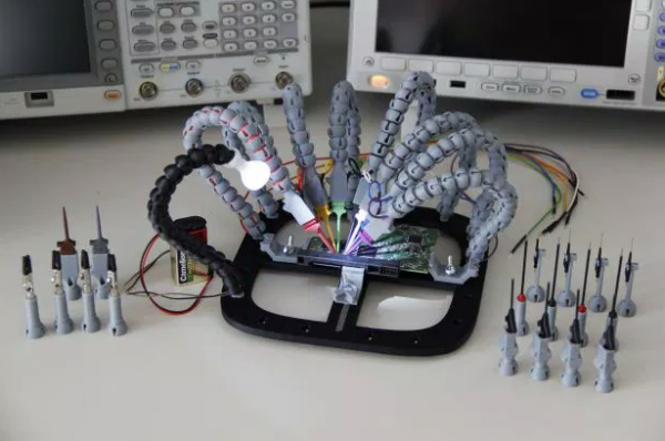
3D Print the Ultimate Helping Hands for a PCB Workstation

pcb_helping_hands

by Giuseppe Finizia @ makezine.com:

I am the Senior Analyst of the Electronic Forensics Unit of the Carabinieri (Italian Military Police) and I deal with technical investigations on seized electronic devices. I spend most of my day in a well-equipped electronic laboratory, but I was lacking a tool for performing technical assessments on printed circuit boards (PCBs). I needed a way to secure small boards on my workbench and place multiple probes across the board for acquiring data from a circuit memory, analyzing an I2C or SPI communication bus using a logic state analyzer, and much more.

3D Print the Ultimate Helping Hands for a PCB Workstation – [Link]

Multifunction biosensor/vital signs monitor for wearables, from ams

150930edne-ams-as7000-iso

by Graham Prophet @ edn-europe.com:

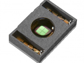
Sensor and mixed-signal IC specialist ams (Graz, Austria) has applied optical detection techniques to produce a sensor capable of accurate heart rate measurement; the company says its device is the first “total solution for 24/7 heart rate measurement for wearables”.

AS7000 is the first in what is to be a family of health/fitness solutions from ams, for wearable devices. The AS7000 solution incorporates a highly integrated optical sensor module accompanied by software to provide the highest accuracy optical heart rate measurements (HRM) and heart rate variation (HRV) readings, backed by opto-mechanical design-in support. The 24/7 reference is to indicate that ams intends the device for products that are worn continuously, rather than (for example) only during periods of exercise.

Multifunction biosensor/vital signs monitor for wearables, from ams – [Link]

DIY Motorized Combo Lock Cracking Device

Combo Breaker is a motorized, battery powered, 3D printed, Arduino-based combination lock cracking device. It is portable, open source, 3D models provided, and exploits a new technique I’ve discovered for cracking combination locks in 8 attempts or less, but in an even more exciting, automated fashion.

DIY Motorized Combo Lock Cracking Device – [Link]

Solar Cells Made Obsolete – 3D rectennas aim at 40-to-90% efficiency

rcj_optical_rectenna_solar_1

R. Colin Johnson @ eetimes.com:

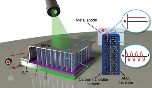
PORTLAND, Ore.–Now before you get all excited by the headline, which is not click-bait according to the researchers, a new kind of nanoscale rectenna (half antenna and half rectifier) can convert solar and infrared into electricity, plus be tuned to nearly any other frequency as a detector. The invention was made at Georgia Tech (Atlanta) and peer-reviewed in today’s issue of Nature Nanotechnology.

Right now efficiency is only one percent, but in the paper (DOI: 10.1038/nnano.2015.220) professor Baratunde Cola and colleagues at the Georgia Institute of Technology (Georgia Tech, Atlanta) convincingly argue that they can achieve 40 percent broad spectrum efficiency (double that of silicon and more even than multi-junction gallium arsenide) at a one-tenth of the cost of conventional solar cells (and with an upper limit of 90 percent efficiency for single wavelength conversion).

Solar Cells Made Obsolete – 3D rectennas aim at 40-to-90% efficiency – [Link]

Samsung launches industry’s first 12Gb LPDDR4 DRAM

5-samsunglaunc

by Samsung:

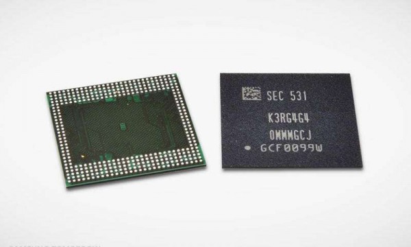
Samsung Electronics announced that it is mass producing the industry’s first 12-gigabit (Gb) LPDDR4 (low power, double data rate 4) mobile DRAM, based on its advanced 20-nanometer (nm) process technology.

The newest LPDDR4 is expected to significantly accelerate the adoption of high capacity mobile DRAM worldwide. The 12Gb LPDDR4 brings the largest capacity and highest speed available for a DRAM chip, while offering excellent energy efficiency, reliability and ease of design – all essential to developing next-generation mobile devices.

Samsung launches industry’s first 12Gb LPDDR4 DRAM – [Link]

One case – over 100 possibilities of usage

obr1758_uvod

We speak about the practical case CTK110EU full of high quality CrV tools sufficient for majority of common operations.

CTK110EU tools set might be easily called as “all-in-one”. Naturally, such all-in-one solution won´t help in all situations which we may face at production or servicing, but very probably it is more than suitable for a vast majority of common operations. Perhaps the biggest advantage of this solution is, that everything is clearly packed in a practical carrying case. So if you have such a case of tools by your hand – in a workshop or car, it´s very probable, that it will be your first choice for any situation.Why just the CTK110EU? Because it is a case from a renowned producer Crescent (a member of APEX tool group, where also the Weller belongs) and contains 110 tools of a guaranteed quality (CrV/ CrNi) and also ergonomically on a very good level.
All, what the case contains can be found in the CTK110EU datasheet.

One case – over 100 possibilities of usage – [Link]

Laser Data Transmission

Lasers have been one of the essential technologies used in industries. It is realized that light outperforms radio in terms of speed and density. It has been used for communications whether in scanning barcodes, reading CD’s and DVD’s. This design is a simple data transmitter that uses a DIP switch to support the transmission of data over a transmission medium. This switch withstands extreme shock, vibration, temperature and altitude.

The circuit works when bits are sent across the receiver using an amplified light where signal is received by a phototransistor. The voltage is converted to digital signal that will be read by the receiver. The one shot multivibrator on both ends used to send 8 clock pulses and will received at the receiving end. The first bit starts the clock and the second bit goes to Serial In/Parallel out IC. Pulse triggering occurs at a particular voltage level and is not directly related to the transition time of the input pulse. Once fired, the outputs are independent of further transitions of the input.

Laser data transmission has various applications that can send voice and video data. This can be made more portable so that users can easily bring the device whenever possible. The device can be easily constructed and integrated to other electronic devices and may be used as a fundamental circuit for electronic finder/trackers.

Laser Data Transmission – [Link]

Making a PCB business card

PCB-BusinessCard-600x439

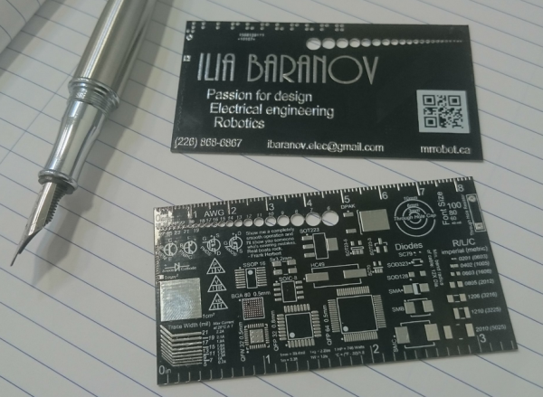
Ilia Baranov has designed a reference business card:

Back of card includes:
Ruler in both 1/10″ and mm.
AWG Hole size gauge (not super accurate due to plating, but that is unavoidable)
Resistor/capacitor/inductor/diode sizes
Common surface mount component sizes
Common electrical symbols and shortcuts/equations
Common conversions
Trace size comparison
Quote from Dune!

Making a PCB business card – [Link]

Hardware Protection – OverVoltage and OverCurrent

Startup-Evolution-Power-Supply-Parameters

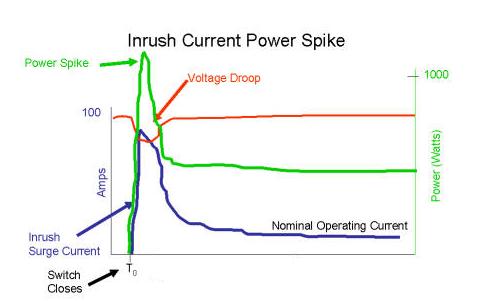
Maurizio @ dev.emcelettronica.com discuss about the different aspects of protecting power supplies from overvoltage and overcurrent.

Power processing is one of the most important aspects on electronic design. The power is unique for a typical system because it gives the system life. Before starting to make the project for a power supply we need to analyze some aspects: Which kind of radio/electromagnetic interference is the device going to face ? What about maintenance requirements? And finally which environment conditions (temperature, humidity, vibrations) will the device be exposed to?

Hardware Protection – OverVoltage and OverCurrent – [Link]

Basic Types of Transistors

In this article we will review the basic transistor types and their function. We will cover bipolar transistor, Junction FET, MOSFET and UJT transistor types. Feel free to comment with other transistor types you know.

Bipolar Transistor
bipolar

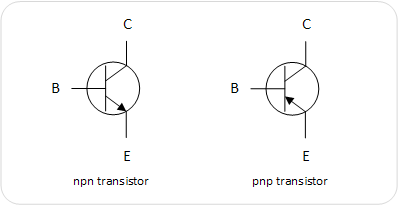
Bipolar transistors are three terminal devices and act like electrically controlled switches of as current/voltage amplifiers. They come in two types either npn or pnp depending on their construction.

NPN Transistor

This type of transistor is normally off, but a small input current and a small positive voltage to its base B (relative to emitter – E) allows a large current to flow from collector to emitter, when collector is in higher voltage than emitter. Normally used in switching applications and amplifiers.

PNP Transistor

This type of transistor is normally off, but a small output current and a small negative voltage to its base B (relative to emitter – E) allows a large current to flow from emitter to collector, when emitter is in higher voltage than collector. Normally used in switching applications and amplifiers.

Junction FET
JFET

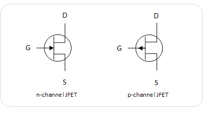
Junction field effect transistors are three terminal devices that are used as switches, amplifiers or voltage controlled resistors. Unlike bipolar transistors they don’t require a biasing current just a voltage to the gate to operate. Another difference with bipolar is that they are normally ON without any voltage to the gate.

n-channel JFET

This type of transistor in normally ON and a small negative voltage to it’s gate – G (related to source – S) stops the large current that flows from drain to source, when voltage of drain is greater than voltage on source. A unique feature is that they don’t need a current to it’s gate and are used in switching and amplifying applications.

p-channel JFET

This type of transistor in normally ON and a small positive voltage to it’s gate – G (related to source – S) stops the large current that flows from drain to source, when voltage of source is greater than voltage on drain. They also don’t need a current to it’s gate and are used in switching and amplifying applications.

Depletion MOSFET
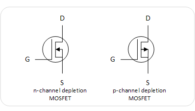
depletion_MOSFET

Metal oxide semiconductor field effect transistors or MOSFETs is a popular type of transistors and when a small voltage is applied to its gate the current flow from Drain to Source is stopped. In contrast to JFETs, MOSFETs have larger input impedance and they draw virtually no current on their gate. There are two main type of depletion MOSFETs, n-channel and p-channel.

n-channel depletion MOSFET

N-channel depletion MOSFETs are normally ON, but a small negative voltage to the gate (related to source – S) stops the current flow from drain to source, when voltage on drain is greater than voltage on source. They need no current at all to the gate.

p-channel depletion MOSFET

P-channel depletion MOSFETs are normally ON, but a small positive voltage to the gate (related to source – S) stops the current flow from source to drain, when voltage on source is greater than voltage on drain. They need no current at all to the gate.

Enhancement MOSFET
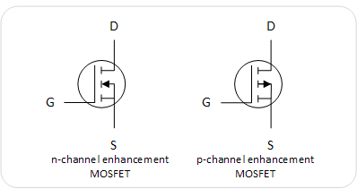
enhancement_MOSFET

n-channel enhancement MOSFET

N-channel enhancement MOSFETs are normally OFF, but a small positive voltage to the gate (related to source – S) allows current to flow from drain to source, when voltage on drain is greater than voltage on source. They need no current at all to the gate.

p-channel enhancement MOSFET

P-channel enhancement MOSFETs are normally OFF, but a small negative voltage to the gate (related to source – S) allows current to flow from source to drain, when voltage on source is greater than voltage on drain. They need no current at all to the gate.

Unijunction FET (UJT)
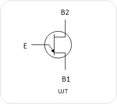
UJT

Unijunction transistors (UJTs) are three terminal devices that are used exclusively as switches and not as amplifiers. Normally a very small current flows from B2 to B1 but if a large positive voltage is applied to emitter – E (related to B1 or B2) increases the current flow, when voltage from B2 is greater than voltage on B1. The larger current from E combines with the smaller current from B2 to B1, thus giving a large current in B1. In this type of transistor the emitter current is the main source of current passing through B2-B1.

TOP PCB Companies