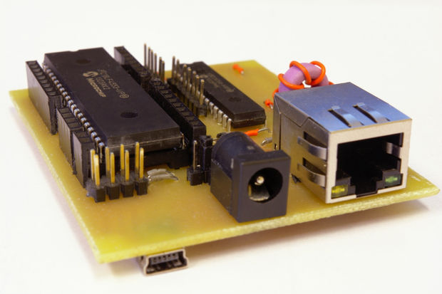
PIC18 Development Board with Ethernet and USB

FMTEZZDID77M637.MEDIUM

by magkopian @ instructables.com:

The development board is based on a PIC18LF4553 microcontroller. The microcontroller features a Full Speed USB 2.0 (12Mbit/s) interface without the need for any external components. Also, it has 32KB of program memory, 2KB of RAM and it supports an external clock up to 48MHz, which is optional because it also has an 8MHz internal clock.

The ENC28J60 Ethernet controller is used to provide Ethernet connectivity to the microcontroller thought the SPI interface. The ENC28J60 has an integrated MAC and a 10Base-T PHY, 8KB of buffer RAM, supports both Full and Half-Duplex modes and it is fully compatible with 10/100/1000Base-T networks.

PIC18 Development Board with Ethernet and USB – [Link]

8T49N004 Programmable Femtoclock® NG with 4-outputs

This design features a fourth generation programmable femtoclock that provides reference frequencies to replace crystals and SAW oscillators in high-performance applications. It is programmable through I2C interface. It has four selectable LVPECL or LVDS via I2C while its FemtoClock NG VCO ranges between 1.9GHz to 2.55GHz. It also meets the standard interface requirements of PCI Express (2.5Gb/s), Gen 2 (5Gb/s), and Gen 3 (8Gb/s) jitter that are low in both clock synthesizers and phase-locked oscillators.

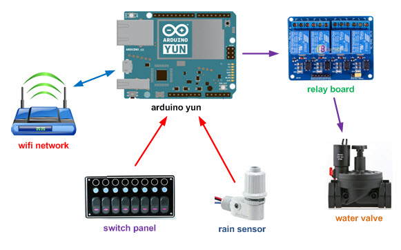
The design is comprised of few components that can be divided into three main areas. First, the I2C interface area that uses optoisolator to ensure the compatibility of the external I2C device to the main clock frequency synthesizer. Second, the main part where the IDT8T49N004I clock generator generates the clock with selectable LVDS or LVPECL outputs. Lastly, the power supply of the device uses a low noise Low DropOut (LDO) regulator that is optimized for fast transient response. It also makes use of reference diodes and capacitor filters that secure the system from possible noise produced from the supply.

The design is applicable to several applications that requires reference clock especially network processors and Application-Specific Integrated Circuits (ASICs). It can improve the overall performance of the device since it makes the device more immune to noise and other undesired system behavior.

8T49N004 Programmable Femtoclock® NG with 4-outputs – [Link]

Homemade x-ray inspector reveals PCB secrets

capture_021

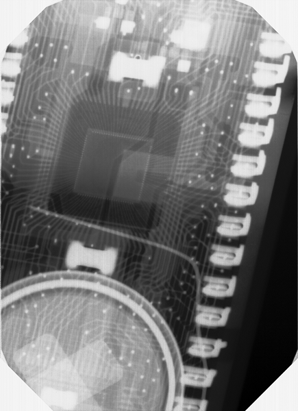
John McMaster has written an article detailing his homemade x-ray scanner:

In some previous posts I talked about getting an x-ray head working, reverse engineering an x-ray sensor, and working with LinuxCNC. In this post I put them all together so that I can take a bunch of x-ray snapshots across an entire PCB. This allows me to more quickly reverse engineer PCBs.

Homemade x-ray inspector reveals PCB secrets – [Link]

Simple and small temperature fan control

FanControl4-600x462

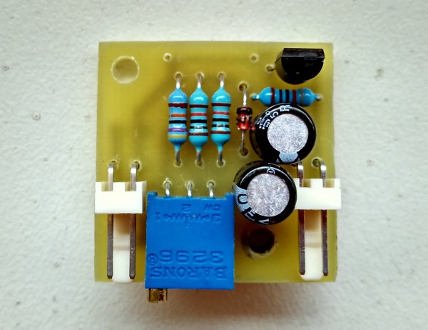
Xristost published a new project, a simple and small temperature fan control:

I published this schematic long ago in this article: Adjustable power supply and since then I made some improvements in PCB to make the board as small as possible. The idea is to be easy to attach the whole board to the heat sink which we want to monitor. The board is only 27mm x 27m

Simple and small temperature fan control – [Link]

Toshiba launches 256-Gbit 48-layer 3-D NAND flash

Toshiba BiCS

by Susan Nordyk @ edn.com:

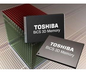
Ready for sampling in September, Toshiba’s 48-layer BiCS (Bit Cost Scalable) flash memory stores 256 Gbits using a 3-D vertically stacked cell structure and 3-bit-per-cell triple-level cell technology. By employing this 48-layer vertical stacking process, BiCS flash surpasses the capacity of conventional 2-D NAND flash memory, where cells are arrayed in a planar direction on a silicon plane.

BiCS also enhances write/erase reliability endurance and boosts write speeds. The 256-Gbit (32-Gbyte) device can be used in a myriad of applications, including consumer solid-state drives, smart phones, tablets, memory cards, and enterprise SSDs for data centers.

Toshiba launches 256-Gbit 48-layer 3-D NAND flash – [Link]

Wireless Nixie Thermometer

FI251XKICRXVI4O.MEDIUM

by christian.ich.7 @ instructables.com:

The Target of this Project was to learn how to use different functions of the atmega:

• Connecting two Atmegas with a wireless connection
• Each Atmega has a Thermometer (DS1621) to read the actual temperature
• Use the sleep Mode of an Atmega
• Controlling a Nixie bargraph In-13

Wireless Nixie Thermometer – [Link]

Arduino Chess Clock

FZ6CGH3ID4CQC6I.MEDIUM

by benhur.goncalves @ instructables.com:

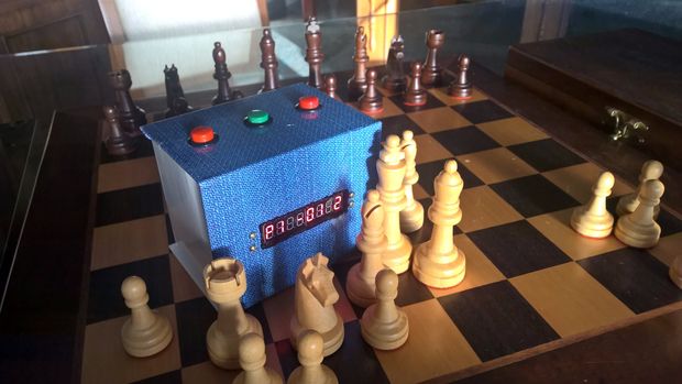
Hey folks! After making an Arduino smartwatch just last week, I received many complaints,or tips, to use a RTC (real-time clock) module. That’s because the Arduino timer is not very precise, it can lose a couple a minutes along a full work day. Luckly, I had one of those modules at my home, I decided to give it a try. However, I faced some challenges along the way, as I can show you here.

Arduino Chess Clock – [Link]

Design & simulate in the clouds

dscloud1

by Michael Dunn @ edn.com:

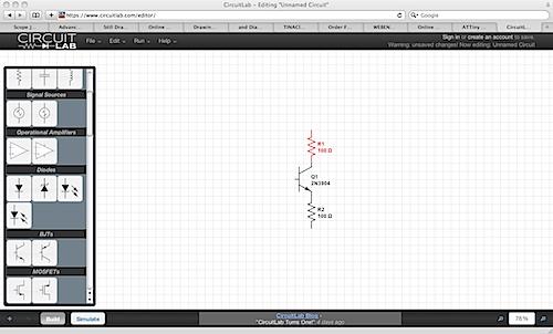
It was a few years ago that I first heard of a free site where you could draw and simulate designs. “What’s the point?” I thought. But, the idea is taking off. Was I wrong?

I questioned the usefulness of this cloud concept because there had already long existed good, free circuit simulators. A quick download, and off you go, drawing and simulating. Why deal with the extra vagaries of service-provider availability, and of course, Internet access?

Well, as with any other cloud-based service, there are advantages, such as being able to work anywhere, on any supported device, and not having to deal with the software directly. And while the services out there now seem mostly suited to exploration, hobby, and simple prototype use, they will keep getting better. Some are arguably already professional grade.

Design & simulate in the clouds – [Link]

Supercap energy density rivals batteries

20150805015959_sol-gel-capacitor2

by Martin Cooke @ elektormagazine.com:

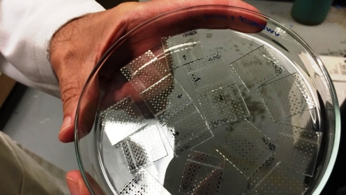
A novel design of supercapacitor using a hybrid silica sol-gel material and self-assembled monolayers of a common fatty acid has been developed by researchers working at the Georgia Institute of Technology. The device is said to provide an electrical energy storage capacity rivaling certain batteries, with both a high energy density and high power density.

The new material is composed of a silica sol-gel thin film containing polar groups linked to the silicon atoms and a nanoscale self-assembled monolayer of an octylphosphonic acid, which provides the insulating properties. The bilayer structure blocks the injection of electrons into the sol-gel material, providing low leakage current, high breakdown strength and high energy extraction efficiency.

Supercap energy density rivals batteries – [Link]

TOP PCB Companies