RS232 or RS485 Module

PIC


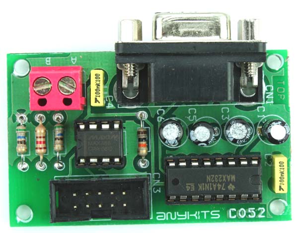
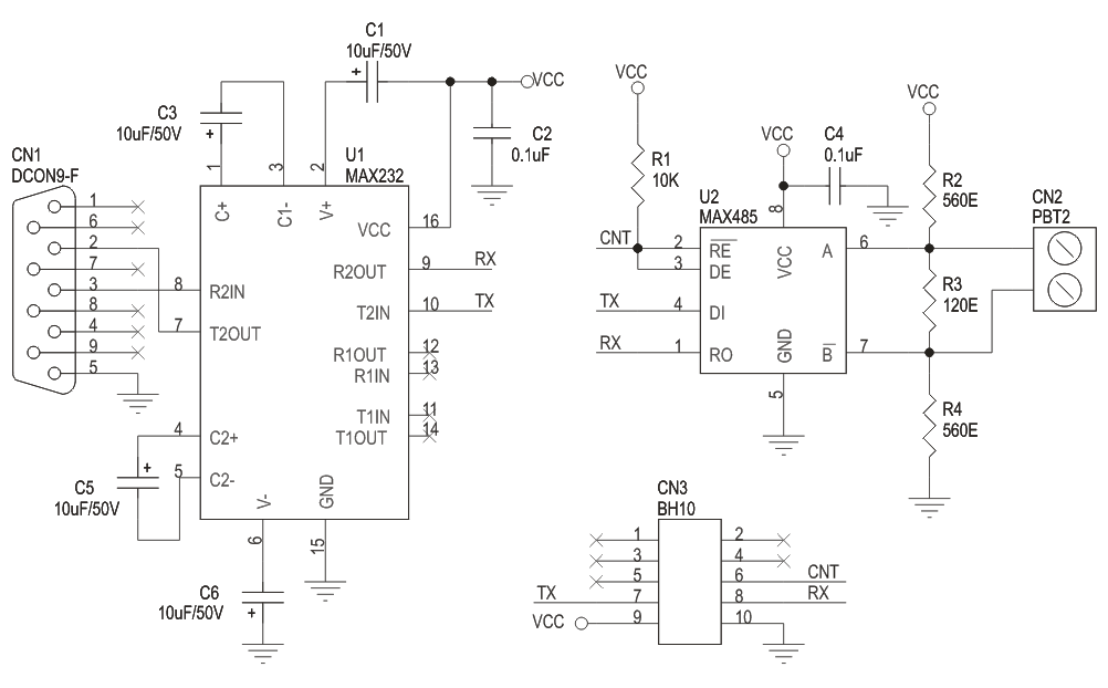
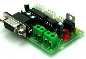
This project is a RS232 & RS485 Interface Board

RS232 or RS485 Board will help you provide a seamless connection of either of the protocol RS232 or RS485 with your interfacing circuit.

Specifications

  • 5 VDC Supply sourced through the Box Header interfacing connector
  • Either of the two communication protocol available by use of individual IC on the PCB
  • PBT type connector for connection of the RS485 link cable and 9 pin female type D connector for interfacing of UART signals to the PC
  • Four mounting holes of 3.2 mm each
  • PCB dimensions 38 mm x 61 mm

Schematic

SCHEMATIC


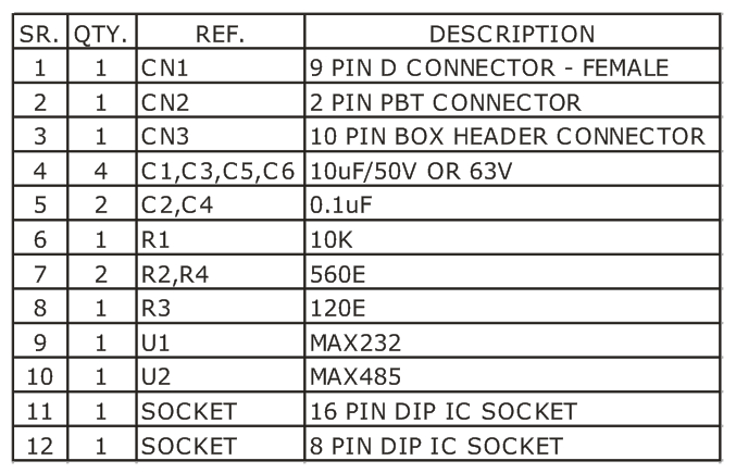
Parts List

BOM


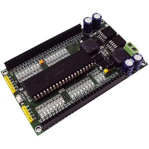
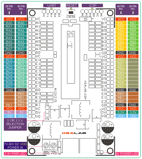
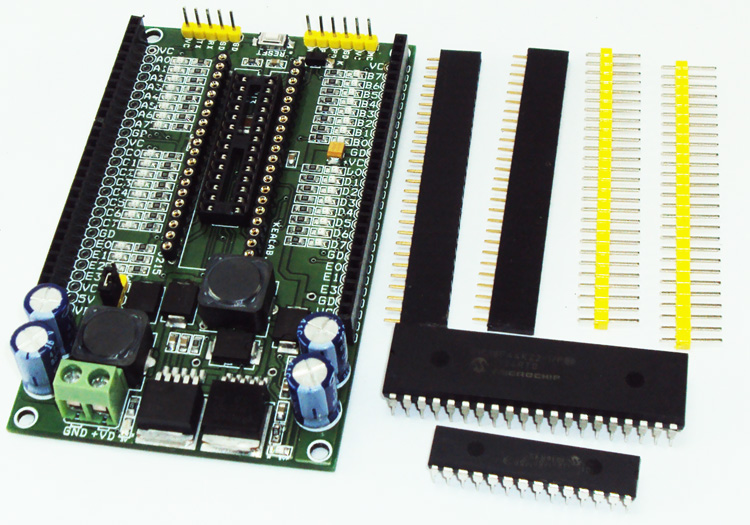
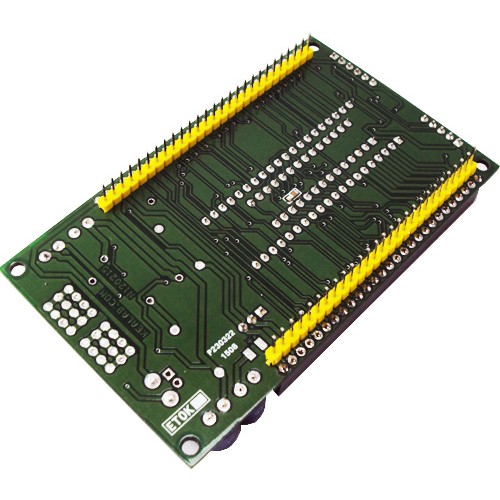
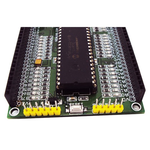
40 & 28 PIN PIC Development Board with ICSP interface

PIC004


This is a PIC 40/28 PIN (DIP) PIC Development / Evaluation board that demonstrates the capabilities of Microchip’s 8-bit microcontrollers, specifically, 28- and 40-pin PIC16FXXX, PIC16F1XXX, and PIC18 devices. It can be used as a standalone demonstration board with a programmed part. With this board, you can develop and prototype using all Microchip’s 40 & 28 PIN PIC microcontrollers that don’t require external crystals (External Oscillator). The on-board connector for UART (RX-TX) allows an easy connection with embedded hardware and peripherals. The board has a RESET switch and status LEDs.

An on-board 3.3 V and 5V DC converter allow using 3V or 5V PICS as this board supports both 3.3V low power and normal 5V operation. All I/O Pins out with female header and male header connectors.

Specifications

  • Power Supply 7V to 36V DC @ 3 Amps
  • 40 PIN PIC18F46K22 & 28PIN PIC18F26K22 DIP Microcontrollers
  • The PIC development platform is exclusively designed to offer full experimenting flexibility to a developer or application engineer for the enhanced range of 28/40 pin 8 bit PIC Microcontroller.
  • Industrial standard 3A Switching regulator brings in safe operation of the board for all types of input supply without overheating.
  • Dual supply (5.0V and 3.3V @ 3A) takes care of all the supply needs of your IO devices and the operating voltage of the board. Independent Supply of 3.3V, 5V, and Input VDD (Input Supply) is always available at header pins.
  • With a single Jumper, you can select the operating voltage of the MCU between 5.0 and 3.3 V
  • PICKIT2 standard ICSP interface is available for ease of programming.
  • Separate IO pins for the UART interfacing available for Serial interfacing.
  • A LED circuit on every IO pin of the MICRO to give you an easy visual status of the pins. Optional and not provided along with the kit.
  • Separate PWR ON indicator for each of the 2 supply (3.3V / 5V) available.
  • Dual Header connector, Male/Female available for ease of interfacing with the outside world
  • RESET switch to reset the onboard MCU.
  • Supply reverse input diode for protection at both 3.3V and 5V  DC-DC Converter inputs

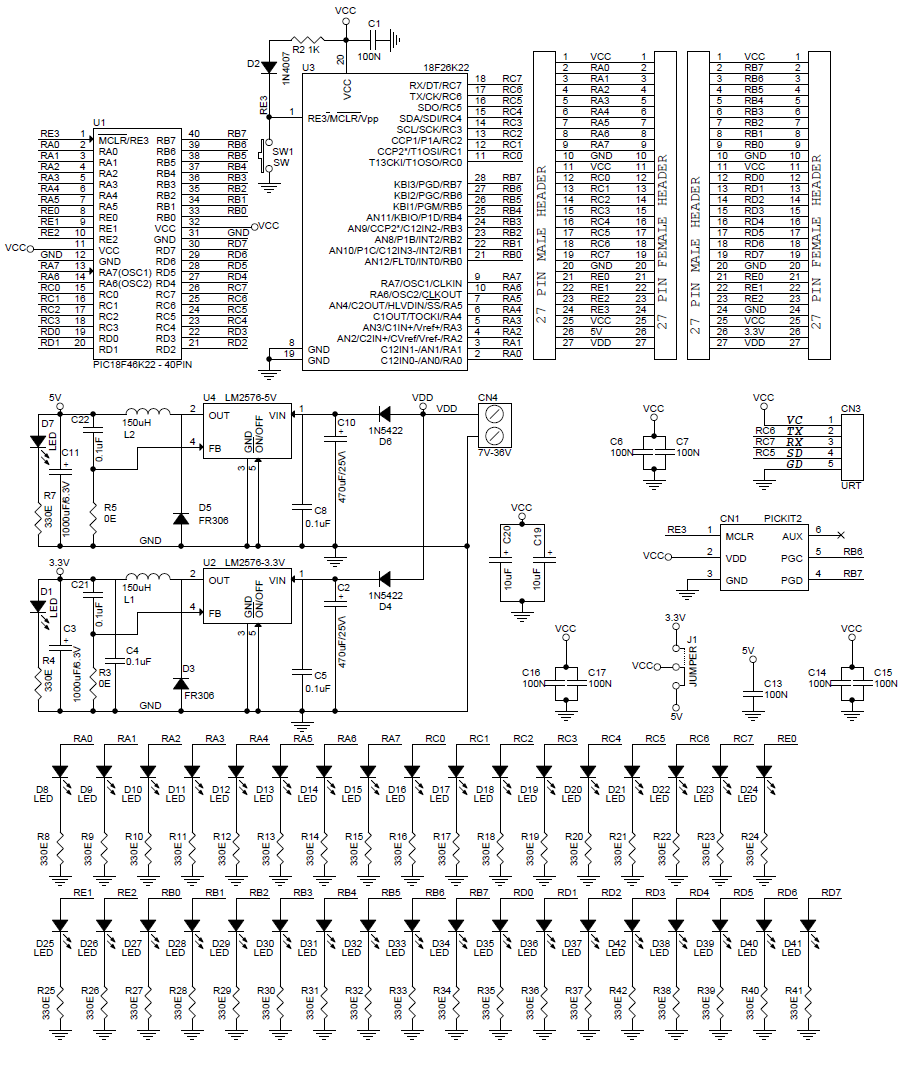
Schematic

schematic


IO Details

I-O DETAIL

Photos

PIC001

PIC002

PIC003

USB Single Cell LiPoly Charger

SAMSUNG DIGIMAX A503

Introduction

Lithium Polymer Batteries are a very common source of power today. Many electronics gadgets have one inside, and they have some reasonable features. I’ve bought great batteries, with different sizes and capacities for my electronics projects. So long I’m using this batteries, coming the problem: charge them.

Charger Version 1

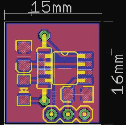
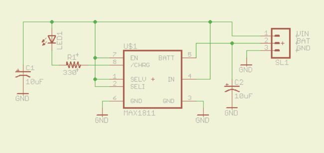
So, we start to find the correct circuit for my DIY charger. After some Google research I found the Maxim MAX1811 IC. It’s a single-cell Lithium battery charger that can be powered directly from a USB or from an external supply up to 6.5V. It’s use a SO-8 Package, easy to solder and can be sampled at Maxim. Other chip features are:

You can select between 4.1V and 4.2V battery regulation point;

• You can select between 100mA and 500mA current drain from USB;

• There’s a open drain pin (pin_8) for signaling end of charge condition (2.5V < VBATT < BATT Regulation Voltage);

• A internal thermal loop limits the MAX1811 die temperature to +135°C by reducing the charging current as necessary.

According to datasheet, MAX1811 is specifically made for USB devices. The minimum voltage to a common USB-powered device may be as low as 4.35V when cable and connector drops are considered. The MAX1811 is optimized for operation at these low input voltage levels. But USB hubs may also provide as much as 5.5V!. At high input voltages (5.5V) and low cell voltages (2.7V), the MAX1811’s thermal loop may limit the charge current until the cell voltage rises.

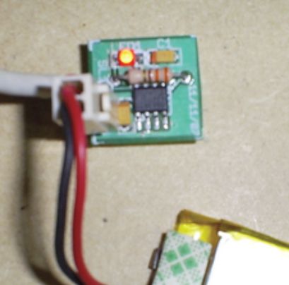
My design uses 500mA was charging current (pin 2 – SELI – pulled up), but MAX1811 only taken this current if the device is a USB powered source. The other parts are two very common tantalum capacitors and a LED for charging indication. LED is ON on charging state, and OFF when it’s end.

Above you see the schematics and PCB of my version 1:
Schematic_1

PCB_1

USB_LiPoly_Charger_5

Charger Version 2

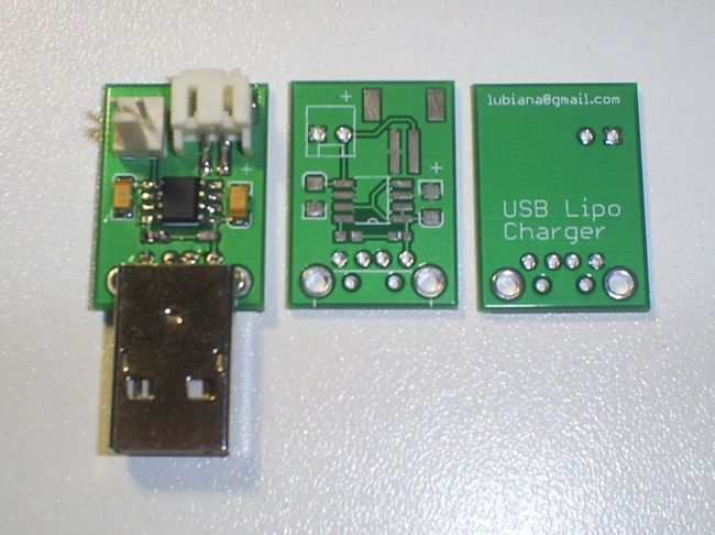
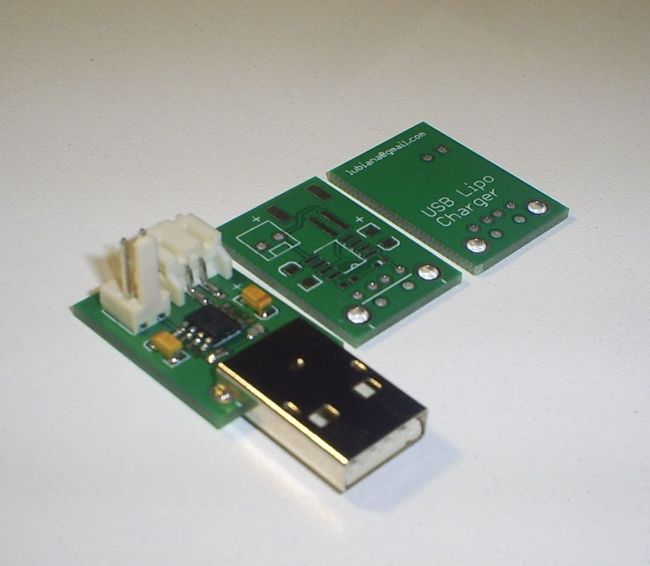
Once I’ve finished the version 1 and tested working fine, I look at the board and think “Why the hell I can’t put a USB Type A male connector on board?”. Well, that’s why there’s some project versions.

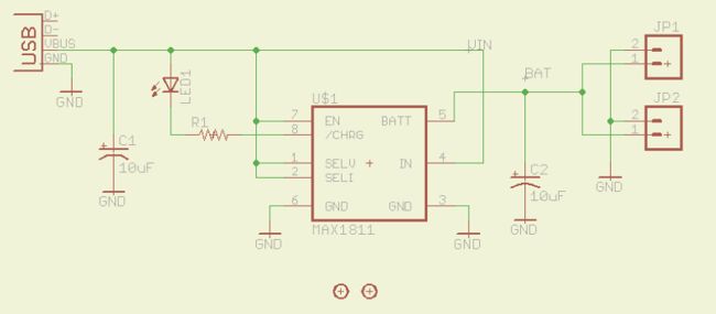
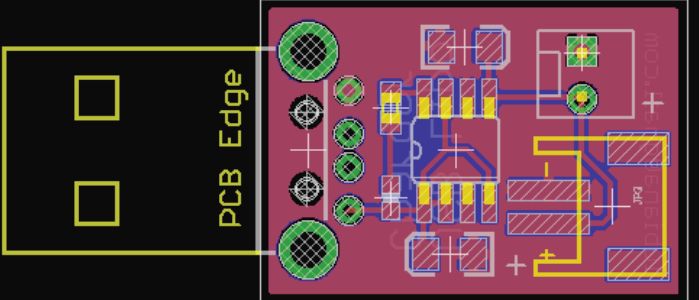
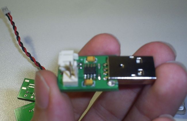
After redesign the circuit, the result was very good, with a new compact board, that now is able to handle batteries with the common JST connector. See the pictures:
Schematic_2

PCB_2

SAMSUNG DIGIMAX A503

Conclusion

Was a first incursion on LiPo chargers, this project end was success to me. The tests show that MAX1811 is a reliable choice and good alternative over other common choices, like MAX1555 IC.

The thermal loop gives some security to device, so you can connect it to your PC or notebook without fear.

The Eagle files can be downloaded from my blog at http://rusticengineering.wordpress.com. Any question, email me.
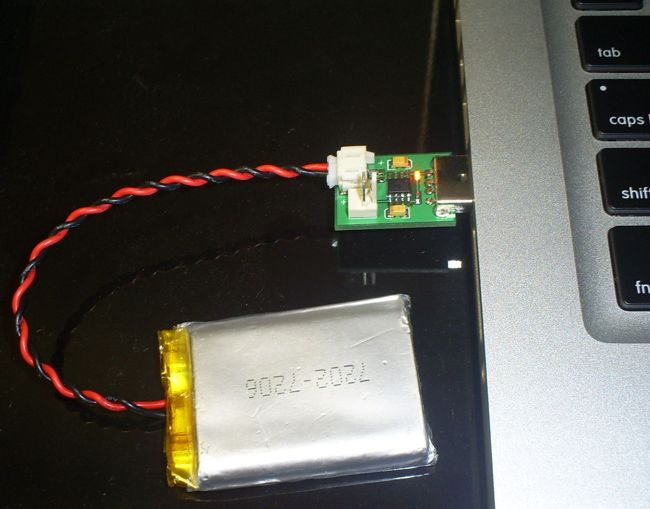
SAMSUNG DIGIMAX A503

SAMSUNG DIGIMAX A503


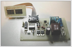
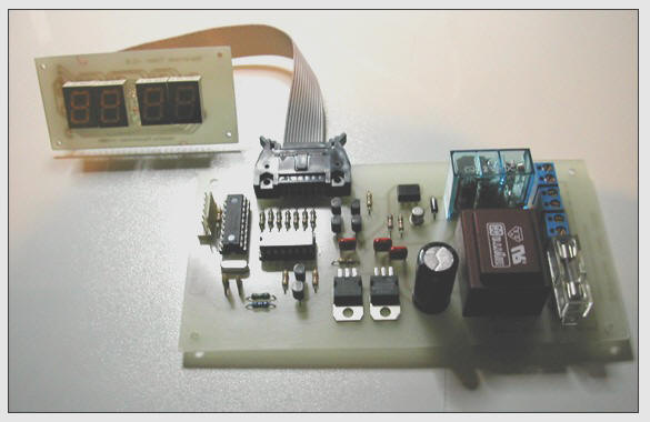
Darkroom Timer v2.0A for PCB Exposure Box


PIC based automatic timer for a PCB exposure box

This is an improved version of the Darkroom Timer originally created by Stan Ockers (1999). Some extra features were added and the PIC code was modified accordingly.

  • Lamp(s) light at start of timing and turn off when timer reaches zero.
  • A set of leds were added between the minute and second leds which blink during timer operation.
  • 7 segment displays include tails for digits 6 and 9.
  • A bicolor led (common cathode) indicates standby (green) and timer operation (red).
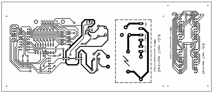
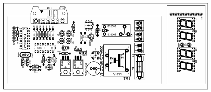
  • Separate PCBs were designed for the led display and the timing system. The power supply is also integrated in the PCB.

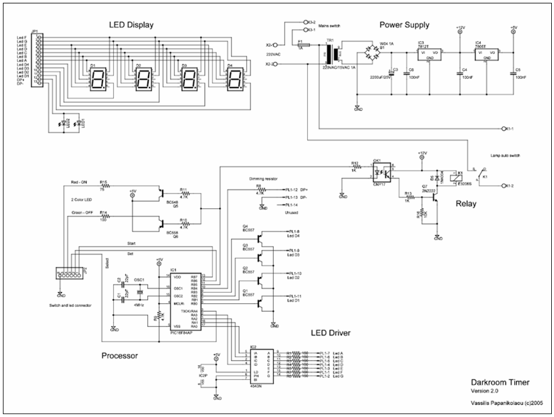
The complete schematic, PCB and silkscreen are available in high resolution pdf format. The component values are clearly indicated on the silkscreen. The modified source code is available in asm and hex format (compiled in MPLAB).

timer_schematic
Darkroom Timer Schematic
timer_pcb
Darkroom Timer PCB
timer_layout
Darkroom Timer Silkscreen

Parts list

System board

R1 – R7              150 Ω  1/4W 5%

R8 – R11           4.7 KΩ  1/4W 5%
R12 – R13         1 KΩ 1/4W 5%
R14                   100 Ω 1/4W 5%
R15                   75  Ω 1/4W 5%
R16                   10 KΩ 1/4W 5%
C1 – C2             22 pF
C3                     2200 μF/25V electrolytic
C4 – C6            100 nF

D5                     1N4001/4004/4007
F1                     1A  Fuse (with socket and cap)
B1                     1A  Bridge rectifier
IC1                    PIC16F84AP Microcontroller (4MHz clock) (with IC socket)
IC2                    74HC4543 BCD to 7-segment decoder (with IC socket)
IC3                    7812 voltage regulator
IC4                    7805 voltage regulator
PL1                   14 pin connector
JP2                    6 pin header
K1                     12V DC / 220V AC Relay
OK1                   CNY17-1 Optocoupler

OSC1                 4MHz Crystal
Q1 – Q4             BC557/558 PNP Transistror
Q5                    BC547/548 NPN Transistor
Q6                    BC557/558 PNP Transistror
Q7                    2N2222 NPN Transistor
TR1                   220VAC/15VAC 1VA PCB Transformer

X1 – X3             2 pin WAGO screw clamp

Led board
D1 – D4              Common cathode 7-segment display
LED1 – LED2        Orange Led 3 mm
JP1                    Not a connector, cable is soldered directly on the back of the led PCB

Box front
Bicolor common cathode led (green-red)
3 push-button switches
Switch connections

Connector X1 is connected to the lamp(s)
Connector X2 is connected to 220VAC mains
Connector X3 is connected to the mains switch

Led board is connected to system board via connector PL1

JP2 pin number - Connection
1 - START Switch
2 - SET Switch
3 - SELECT Switch
4 - Green bicolor led anode
5 - Red bicolor led anode
6 - Ground

Operation

  • Connect the three switches between pins 1, 2, 3 and ground (pin 6). Bicolor led common cathode is connected to ground (pin 6).
  • Start switch starts the timer. Pressing Start again (before or after timer reaches zero) resets the timer to its initial value.
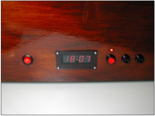
  • Set switch sets the time of the current memory position. This is done in a digit‑by‑digit fashion.
  • Select switch rolls the time values through the 15 memory positions.

Photos

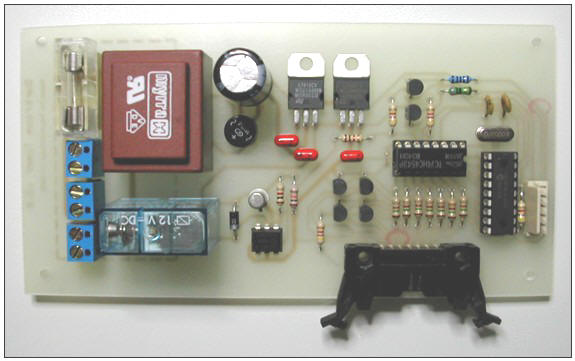
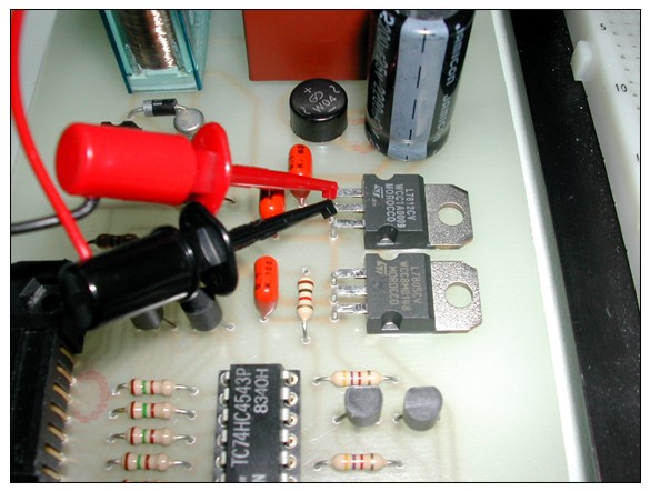
photo1

The system board

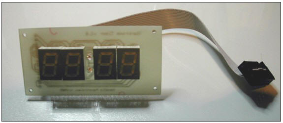
photo2

The led board

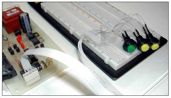
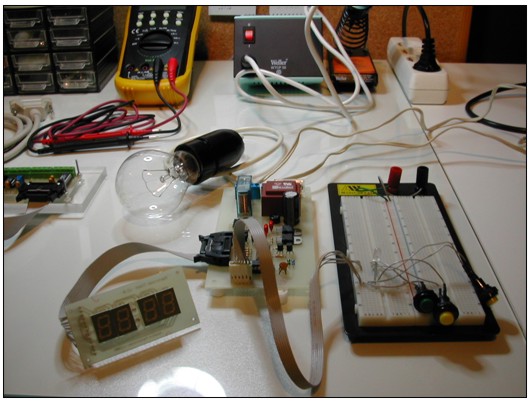
photo4

Connection of switches and bicolor led (JP2) done in breadboard
Normally switches and bicolor led are attached to the front of exposure box

photo5

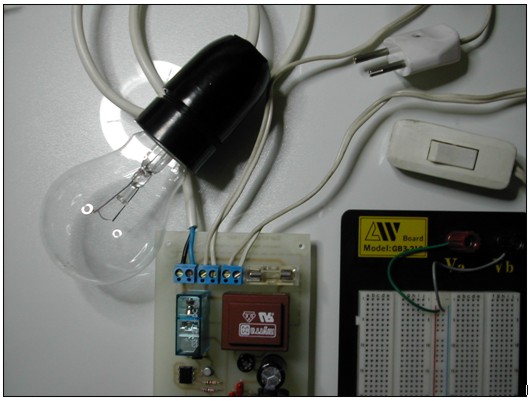
Board testing with externally applied DC on the 7812 regulator (for safety reasons)

photo7

photo6

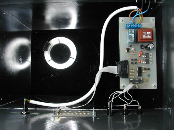
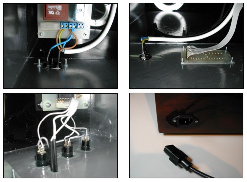
Photos of the Darkroom timer installed on the exposure unit

photo9

photo10

The system board, LCD board and switches installed
Notice the common ground for push buttons and bicolor led (JP2 Pin 6)

photo11

The darkroom timer during operation

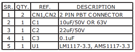
3.3V Voltage Regulator

C026-500x500-500x500


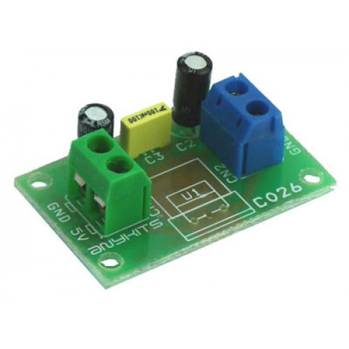
This project is a 3.3V Voltage Regulator

Description

This project  will provide 3.3 V @ 800 mA DC Regulated Supply.  The project is based on the LM1117 Low-Dropout Linear Regulator. The LM1117-3.3 is a low dropout voltage regulator with a dropout of 3.3V @ 800mA of load current.

Specifications

  • Input – 5 to 15 VDC
  • Output Current/Voltage 0<Iout<800mA, 4.75V<Vin<12V
  • Output – 3.3 V @ 800 mA regulated low ripple DC voltage
  • Current limiting and Thermal shutdown circuit protection (provided by IC feature)
  • Filter capacitors for low ripple DC output
  • Power Battery Terminal (PBT) for easy connection of input and output
  • Four mounting holes of 3.2 mm each
  • PCB dimensions 34.29 x 23.34mm

Schematic

SCHEMATIC


Parts List

BOM

Gerber View

RS232 to RS485 Module

C020


This project is a RS232 to RS485 interface module

Description

This project provides a simple and easy solution to connect your computer to a RS485 Network in either Receiver or Transmitter mode.

This circuit has been designed around popular MAX232 and MAX485 interface IC.

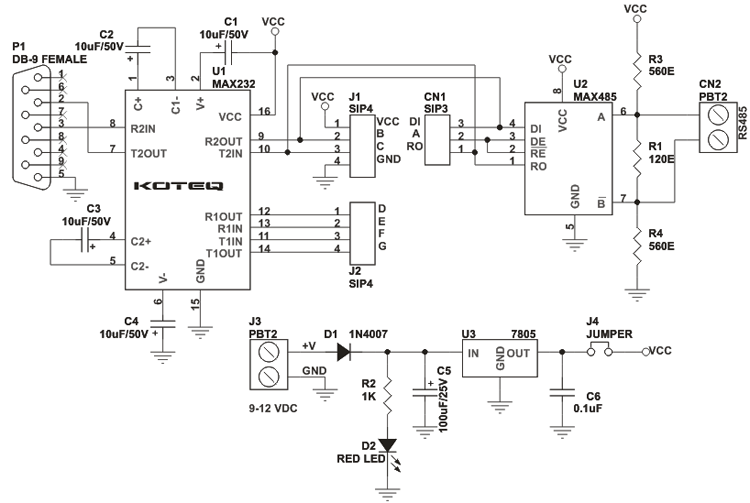
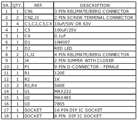
An Onboard 9 pin female “D” connects this PCB to the Serial Port cable (not supplied with the Kit). Connector J1 and J2 provide the MAX232 IC input/output (IO) and Connector CN1 provide MAX485 IO. An optional Power Supply section can provide regulated 5V DC to the circuit and can be included to power by bridging Jumper J4. LED D2 provides visual indication of power on this board and Diode D1 prevents against reverse polarity connection of power supply at J3. This circuit can also work on 5V supply from the host interface which can be provide through J1 in which case you need to remove Jumper Link @ J4. Connector J2 provide extra connection of the other set of level shifter with in the MAX232 IC.

RS485 cable is to be connected at Connector CN2 and are impedance matched with Components R3, R1 and R4.

Terminal marked “A” on CN1 is the Receive / Transmit control Pin for the RS485 flow control. Pulling this pin to Gnd will enable the Receiver on the RS485 and Pulling it High (connecting it to Vcc) will enable it to work in the transmit mode.

To connect the MAX232 IC to the MAX485:

  1. Connect Pin marked C on connector J1 to Pin marked DI on connector CN1
  2. Connect Pin marked B on connector J1 to Pin marked RO on connector CN1

Connector J1 connects to the Host for power supply and serial In/Out signals.

  • A – Provides data from the Computer to the Host (RXD)
  • B – Provides data to be sent to the Computer from the Host (TXD)

Specifications

  • Supply input 5-12 VDC Max

Schematic

SCHEMATIC

Parts

BOM

12V Lead Acid Battery Voltage Monitor

D005-500x500-500x500

This project is a 12V Lead Acid Battery Voltage Monitor

Description

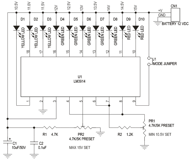
12V Lead Acid Battery Monitor is a simple project which tells you the voltage of your Lead acid battery visually with the help of 10 LED’s.  This project is based on the popular LM3914 IC from Texas Instruments.

The LM3914 senses the voltage level at the input pin and drives the 10 light emitting diodes based on the voltage detected on input connector. Circuit works on same battery, doesn’t not require separate supply input. Jumper is used to select the DOT mode or bar graph mode.

Specifications

  • Supply input 15 VDC Max
  • Maximum and Minimum range selectable with onboard preset
  • Output 10 LED’s
  • 2 Types of display Bar and Dot selectable by a jumper
  • Very low current consumption, typical 100 mA
  • Header connector for connecting power / voltage in
  • Four mounting holes of 3.2 mm each
  • PCB dimensions 37 mm x 75 mm

Schematic

SchemAtic


Parts

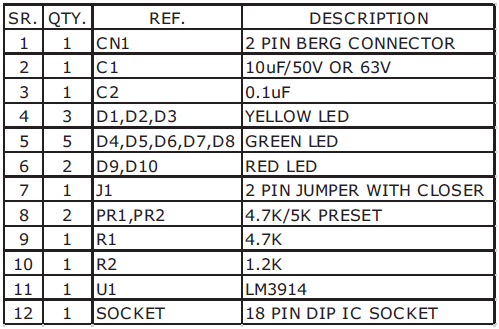
BOM

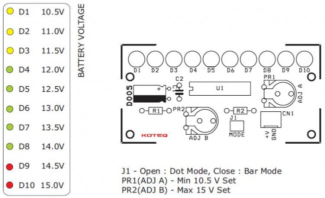
Configuration

Voltage

Multipurpose 18 PIN (16F628A) Microcontroller development board

photo


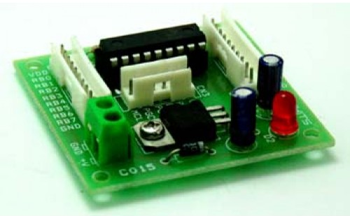
This is a 18 PIN (16F628A) microcontroller development board

Description

This project is a versatile, configurable, and cost effective development board available for the 16F628A or other 18 PIN Microcontroller from Microchip. The board has simplest form with all the Port pins terminating in a Relimate connector (Header Connector) for easy connection to the outside world.

Some of the key benefits of this Development board are :

  1. Well Marked ICSP connecter for easy programming to the MCU on Board.
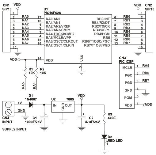
  2. Pull up resistors for MCLR and RA4 Port pins on the PCB. 
  3. Diode D1 helps against reverse polarity connection. at CN4.  Power On LED D2 displays Power on the PCB and the Voltage Regulator IC –U2 7805 ensures regulated power to the microprocessor and other devices connected to this board.
  4. All Port Pin Connector are capable of providing DC supply to the add on cards. Please ensure that you calculate your current requirement before sourcing this supply from this PCB. No short circuit protection is provided at these outputs.

Power Supply 7-12V DC

Schematic

SCHEMATIC


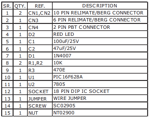
Parts List

BOM


TOP PCB Companies