Features
- LED matrix display 40×7;
- Display of clock, calendar, inside and outside temperature, custom text massages;
- Automatic Daylight Savings Time;
- Capability of keep the real time clock works correctly for more than one week without power supply.
- Clock automatic calibration a software function, adding or subtracting a preset number of seconds (0-59) once time per day, improving clock accuracy;
- Inside temperature measurement (-40 ÷ +75) °C, ±0.5 °C accuracy;
- Outside temperature measurement (-40 ÷ +75) °C, ±0.5 °C accuracy;
- Displaying minimum and maximum temperatures reached;
- Supports static and running massages with different effects;
- Full Cyrillic and special symbols supports;
- External memory for 10 custom messages, freely configurable via PC software;
- Bult-in fixed messages;
- Automatic brightness control;
- IR remote control for settings and massage selection;
- Power supply: 12 ÷ 24V DC;
- Front panel dimensions 305×69 mm.
Schematic Description

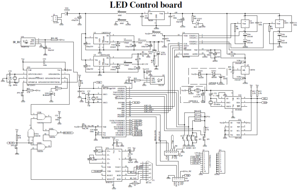
The device is separated of two parts named LED control board and LED display board. Two PCBs are designed to fit together one behind other using two sets of dual row connectors and 4 spacers. One of this connector is used for electrical connections, while the other one is used only as mechanical connecting element.
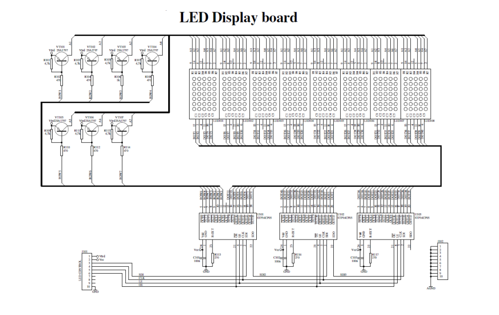
The core of the device is the microcontroller PIC18F252 (U9). The microcontroller controls all functions of device, generates the whole algorithm to control the LED matrix. LEDs are connected in matrix 40×7. The columns tie together the cathodes of LEDs and rows tie the LEDs anodes. The LEDs are dynamically controlled row by row. To safe space and number of components, the LEDs are driven with specialized LED driver STP16CP05 (U101-U103), produced from ST Microelectronics. Each one of these IC contain 16-bit serial-in, parallel-out shift register, latch register and 16 constant current output channels. Outputs are open drain type, allowing connection of a load supplied with up to 20V supply voltage. The constant current for all outputs is set from an external resistor (R115-R117) connected to pin 23. Its value set the LEDs current from 5 to 100mA.

In this application, the three LED drivers are connected in cascade and controlled from the microcontroller over SPI protocol. The microcontroller sends a 48-bit word, controlling one row at the time. The 40 LSB represent LED states (1-On, 0-Off) in the row and controlled their cathodes. The 7 MSB are controlled the anodes through the 7 driver transistors (VT101 VT107). The 40th bit remains unused. The microcontroller sends this 48-bit word each 1ms. There is 7 row cycles for displaying each row plus one blank cycle, used for process the temperature measurements. Therefore, the refresh rate of display is 125Hz. To control the display brightness is used the outputs enable (OE) pin.
Each row cycle begin with logical 0 on OE pin (outputs are enabled). Depends on the desired brightness the duration of enable signal is changed, using the microcontrollers on-chip PWM module.
Note, that the numbers of columns and rows are not connected in sequential order to the corresponded pins of ICs (U101-U103). This is done due to simplify the design of PCB. The LEDs corresponded bits are rearranged by software to fit them with their physical order.

Real-time clock / calendar
The real time clock is implemented with U10 – PCF8583. This is a clock / calendar / alarm circuit with I2C interface and on-chip 32768Hz oscillator. The PCF8583 contains all necessary counter registers to provide real time clock and date information. Its power consumption is very low (typical supply current is 10�A) and operate in wide range of supply voltage from 1 to 6V. These features give a possibility to supply the real-time clock for a long time using a small lithium battery or even with a back-up capacitor. Both options are available in the designed PCB. The footprint for lithium battery is suited for 2032 type socket.
The experiments using 1F back-up capacitor shows that the clock remain active more than a week after turning-off the power supply. The diodes VD10, VD11 and VD12 should be Shotkey type as shown in the schematic, due to their low drop forward voltage. Trimmer-capacitor C21 is used to adjust the oscillator frequency at 32768Hz. For I2C communication is used the Master Synchronous Serial Port (MSSP) module in PIC18F252. This module is set in I2C master mode. On the same bus an external EEPROM (U11) can be connected to expand capacity of data storage.
Note, that the numbers of columns and rows are not connected in sequential order to the corresponded pins of ICs (U101-U103). This is done due to simplify the design of PCB. The LEDs corresponded bits are rearranged by software to fit them with their physical order.

Note, that the numbers of columns and rows are not connected in sequential order to the corresponded pins of ICs (U101-U103). This is done due to simplify the design of PCB. The LEDs corresponded bits are rearranged by software to fit them with their physical order.
External EEPROM
On the same I2C bus an external EEPROM (U11) can be inserted to allow storage of custom messages. This is a standard serial EEPROM (32K x 8) type 24LC256 or some equivalent. Firmware is written on that way that the device can work without this EEPROM. In this case the display will show only built-in messages.
Temperature measurement
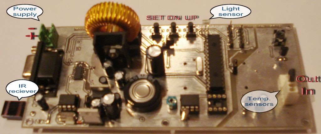
For ambient temperature measurement are used LM35 sensors (U5, U6). They are factory calibrated directly in ° Celsius. The output response is 10mV/°C. The supply voltage should be between 4 and 30 Volts. To make a full-range temperature measurement, a negative voltage must be applied to the output through a resistor (R4 and R5). To ensure this requirement, the ground pins of the sensors is connected to the analog ground through two diodes (VD4,VD5 and VD6,VD7), which pick them up with approximately 1,4V. In that case the Vcc (+5V) power supply is not enough for LM35, so additional voltage regulator is need it to use – U1 (78L09).
The signal from sensor is taken between the output and negative pins of LM35. The voltage between these two pins is bipolar with polarity dependant on the measured temperature sign. The sensors could be connected with external three-wire cables. Software is designed to show inside temperature from U6 and outside temperature from U5.
A/D converter
Both LM35s outputs are connected to U4 – MCP3302. This is a Successive Approximation Register (SAR) analog to digital converter. It provides 13 bits resolution (12 bits plus one sign bit). The MCP3302 has 4 analog inputs, which can be configured either as 4 single ended or as 2 differential inputs. The application requires 2 differential inputs to convert both bipolar voltages from the LM35 temperature sensors. As a reference voltage is used U7 LM336-2,5. Its output value need to be adjusted at 2,55V using trimmer-potentiometer RP1. VD8 and VD9 are used for temperature compensation.
The MCP3302 has an SPI interface, using four signal lines. These lines are under software control from the microcontroller (U9). To ensure accuracy analog ground is separated from the digital using small ferrite beam (L6). This is an SMD type Z600 ferrite beam in 0805 package. The same type are used to decouple the power supply for A/D converter and for temperature sensors and reference voltage (L4 and L5 respectively).

To increase the accuracy and stability of the indication, a modified average filter is applied. The microcontroller get samples from temperature measurements on each second and the values are stored in a buffer. When 10 measurements are stored, microcontroller subtracts the highest two and the lowest two values. From remain six values is calculated an average sum. Then to stabilize the display reading, a slight deadband is applied to the average sum.
Brightness control
For an automatic brightness control is used U8 (TSL257) light-to-voltage converter. Its output voltage is directly proportional to light intensity on the built in photodiode. The voltage from the light sensor is measured using an on chip microcontrollers ADC. The result influences to the PWM module from where the LED panel is changed its brightness. To avoid unwanted blinks of display, a slight software delay of PWM control is applied.
IR remote control
An additional feature of device is the possibility to be controlled using an Infrared remote control. It allows device to be installed on a place with difficult access. The decoder is implemented with microcontroller PIC12F675 (U52) and designed to work with a standard TV remote control, matching RC5 protocol. This protocol is supported from TV Philips. The decoder received a demodulated digital signal from IR receiver TSOP1736.
The software decodes the received command and transmits it to the main microcontroller U9 over an asynchronous serial connection. The LED VD51 is blink once on each recognized command. The main microcontroller (PIC18F252) receives commands from IR decoder using its hardware Universal Synchronous Asynchronous Receiver Transmitter (USART) module. Because the same module is also used for RS232 connection to the PC, RXe signal is multiplexed between the U52 output or U71 (MAX232) output. The switch is realized with 4 NAND elements in U53 (74HC00).
Power supply
The device is needed of three different stabilized supply voltages: Vcc (+5V) for main part of schematic, Vled (+2,5V) for LEDs anodes and a +9V for temperature sensors. For highefficiancy Vcc (+5V) and Vled (+2,5V) are provided using a step-down regulator. For a +5V is used U2 (LM2575-5.0) and for Vled is used U3 (LM2576-ADJ). Because of low consumption from the +9V it is implemented with low power version of standard linear regulator 78L09. Vth1, VD14 and R18 realized overvoltage protection. If the voltage of Vcc exceed the zener diode voltage plus thyristor gate voltage the thyristor starts to open and gives short circuit Vcc to ground. This protects all of integrated circuits from accidentally raising the supply voltage. Note, that the external power supply must have a fuse or current limiter. Of course, this protection circuit is not necessary, but strongly recommended, especially in the stage of testing. Other two power supplies are not so critical if the voltage is increased. The LED drivers outputs can work with up to 20V load and limits the current through the LEDs. The ICs LM35 and LM336 also can work with higher than 9V power supply.
It is necessary to pay attention to the Vled voltage. Its value is very important due to the power dissipation from the LED drivers. In this case are used super bright red LEDs dot matrix modules 5×7 (TC20-11SRWA). The LED forward voltage Vf is 1,85V at 20mA. Its not a problem to use other types of LEDs. For reliable work the Vled should be 0,5-0,7 higher than the Vf. But not to be much more higher, because the power dissipation from the drivers will increase and a thermal shut-down protection will be activated. To calculate the Vled use the next formula:

where R2 is between 1 and 5 k .
It is also need to choose a proper value for LEDs current. The current is set with R115, R116 and R117 resistors, connected to pin 23 (R EXT) of LED driver. The showed value (270 ) set the current at approximately 80mA per output. Because the duty cycle of each row is 1/8, the average current through the LED is 10mA. See the STP16CP05 datasheet for output current resistor set. For convenience of changing these resistors, the footprints of R115 and R116 are duplicated next to R117, named R115 and R116.
Display functions
The display settings are adjusted from the user with three local buttons S1-S3 or by Philips TV compatible IR remote control. The meaning of the local buttons are as follows: S1 – UP; S2 – DOWN; S3 – SET. The available buttons from IR remote control are as follows:
- PROG UP: equivalent to local S1 (UP),
- PROG DOWN: equivalent to local S2 (DOWN),
- MENU or MUTE: equivalent to local S3 (SET),
- 0
9 directly select messages,
- VOL UP, VOL DOWN: Move cursor in Clock settings mode forward or backward respectively.
After Power on the display enters in normal mode of operation, showing continuously the last selected message. The values for temperatures are unavailable for the first 10 seconds. Instead of temperature the display will show F -.–. If this message is shown after this period, it is an indication for a fault temperature sensor.
To select other message press directly one of digital buttons (0
9) on IR remote control, or press one time SET, select the message number using UP/DOWN buttons or digital buttons and press again SET. If an external EEPROM is placed on the PCB and a valid message is written to selected corresponded number the display will show it. If an external EEPROM not installed or the selected number is empty or deleted the display will load a message from built-in memory. Note, that to use the external EEPROM, the setting in the Service menu (extEEP), must set to Y (enable).
To show MAX/MIN temperatures during normal mode of operation press UP or DOWN buttons. At first time the display will show Maximum or Minimum reached Outside temperature. To show MAX/MIN inside temperatures, press UP or DOWN buttons for the second time (no later than 5 seconds). Each time you press two times the same button UP or DOWN the display switched between Inside and Outside values. In five seconds the display will return in normal mode of operation. To reset values manually, while in MAX/MIN mode press SET button. A confirmation message RESET?: appeared. Using the buttons UP/DOWN select Y (Yes) to confirm or N (No) to reject and press SET. Note, that MAX/MIN temperature function is not available for the first 30 seconds after power on.
Configuration menu
In normal mode of operation press two times SET button. A Config is appeared on display. Using UP button the display shows the following options: Time -> Bright -> °Reset -> PC conn. -> back. The button DOWN walks through the same options in reverse order. To return in normal mode select press SET button when back or Config label is showed. If none of buttons is pressed for more than 10 seconds, display will automatically return in normal mode.
-Time: Press SET to enter in set Time and Date mode. Display shows clock and tens of hours are flashing. Set the value using the digital buttons (0
9) from IR remote control. After entering the value, the display automatically selects the ones of hours. In the same way successively enter values for minutes, day, month and year. The day of the week is calculated automatically. Alternatively, the values can be set using UP/DOWN buttons and button SET to switch to the next step. To skip the steps forward and backward use buttons VOL UP and VOL DOWN from IR remote control only. To exit from Time and Date settings mode without changes, press repeatedly VOL DOWN until Time label appeared.
After entering the value for years press SET button to enter in mode of confirmation the new clock value. The new time and flashing OK is displayed. When the button SET is pressed again the new value of clock and date will apply, the seconds set to :00. If an incorrect value was entered, press UP button to return in begins. To discard all changes and return to configuration menu, press DOWN button.
-Bright: Press SET to enter in set Bright mode. Display shows Bright and a digit for bright degree from 1 (minimum) to 8 (maximum) or A for automatic mode. To select a new value for the bright use buttons UP and DOWN to set one of eight degrees or auto mode. From the IR remote control the values can set directly with digital button (1
8) or 0 for auto mode. Press SET again to exit and return to normal mode. The bright setting is stored into built-in EEPROM.
-Reset: This setting switches between automatic or manual mode of reset MIN/MAX temperature registers. When °Reset A is showed on display the registers for MIN/MAX temperature reached are reset on every day at 00:00. When °Reset M is showed on display MIN/MAX registers are reset only manually. To switch between auto/manual modes press SET. The setting is stored into built-in EEPROM.
-PC Conn.: Use this option to connect the display to a PC via RS232. The Message Editor can operate with display only in PC connection mode. When PC Conn. is selected, press a SET button. A confirmation message Contin?N is shown, asking are you sure to continue entering in PC mode. Use buttons UP and DOWN to select Y to confirm or N to exit from this function. If you select Y and then press SET, the display will enter in PC mode and RS232 connection will activated. Once you entered in PC mode the IR remote control is deactivated. To return in normal mode of operation and activate the IR remote control you have three options: press a local button SET, click on Disconnect button in Message Editor software or
restart the device. During this mode of operation a message PC mode is shown permanently on display. During read and write operations the display may start blinking for a short time.
Message Editor Software. First ensure that the display is in PC mode of operation. From drop down menu select a COM port to which cable or USB to RS232 converter is connected. Click on Connect/Test button. If everything is OK, software shows a message The display is connected and display controls become active. If an error message occurs The display is not responding check all conditions mentioned above and try again. Only messages from external EEPROM can be read and modified. Each operation of read, write and delete message is applied to the selected message only. Upload button is read the selected message from an external EEPROM and put it in Message section. Download button sent a prepared message to displays EEPROM. A Delete button deactivate selected message. The content of message remains in memory, but marked as deleted. This means that the display will show a message from built-in flash memory, not from external EEPROM. To activate the same message again,
upload and then download it. To construct a new message sequence showing different data and effects, use drop down menus, from where you can add a message text and commands. The maximum length of message is 250 characters, which includes all symbols and commands. Configured message can be stored to a text file with *.msg extension.
Service menu
Service menu is useful during the initial start-up and testing the device. To enter in service mode press and hold local buttons S1 and S3 until Service text is displayed. Alternatively from IR remote control: in Config mode, press Power/Stand By button. To return in normal mode press SET button while the display shows Service. Use UP or DOWN buttons to select one of test functions: ASCII, external EEPROM, RTC auto correction, Light sensor, PWM output, ADC channel 1, ADC channel 2, IR commands, Firmware version.
-ASCII: Shows display representations for whole ASCII table. Press SET to enter in this mode. The display shows for example 4A (J) a hexadecimal address and corresponding ASCII symbol in brackets. Use UP/DOWN buttons to scroll through the all addresses. To exit from this function press SET.
-External EEPROM: This function is used to enable (Y) or disable (N) the external (I2C) EEPROM. In this mode press SET button to alternate the setting: extEEP:Y or extEEP:N. If the external EEPROM is disabled the display will show only bult-in messages nevertheless, that in EEPROM is written an active message. This setting is stored in built-in EEPROM.
-RTC auto correction: This function will add or subtract a preset amount of seconds at 4:30 am every day. This will automatically correct the time corresponding on how many seconds the real time clock is run fast or slow per 24 hours period of time. To set the correction value press SET button. With UP and DOWN buttons set the value from -59 to +59 seconds. To disable this function set 0. The selected value is written in built-in EEPROM.
-Light sensor: Shows two values: A a row ADC value (8-bit, integer) read directly a voltage from Light sensor, F a filtered value from Light sensor.
-PWM Output: Shows the actual pulse width value (8-bit integer) controlling the bright of LEDs. The value 0 is corresponding to maximum bright, while the value 200 is corresponding to minimum.
-ADC channel 1: Shows the 16-bit signed integer value read from external ADC, differential channel 1. This channel is connected to an outside temperature sensor. On the left side a letter o is showed with an index from 0 to 9. This is the input buffer memory index. Press SET to switch showing a filtered value (integer with sign before converted in Celsius degrees).
-ADC channel 2: The same as ADC channel 1 for inside temperature sensor.
-IR commands: Shows for a short time a decoded command from IR remote control unit. This is a converted command from U52 (PIC12F675), not directly read from IR remote control.
-Firmware version: Shows current firmware version loaded in PIC18F252.
In conclusion
To start the schematic are not required any special adjustments. If the device is assembled properly and two microcontrollers are programmed it will run right away. U9 can be programming with one of two available connector J4 or J4A, depending on the programmer type. It is possible need to disconnect the Vcc from U9, during programming. For that purpose is provided JP1. The U52 must be program externally. Some programming tools may require do not put capacitor between MCLR pin and ground (C16). Note, that the two double row connectors connected the two boards are SMD type. The clearance between the pins is 2,00mm not 2,54! The jumpers JP2, JP3, JP51, JP52 are reserved for some test functions and no needed to be installed. This is a demonstration device. I am open to any ideas and issues concerning the project.
Dont hesitate to write me at: vasilev_ivailo @ abv.bg


