DDS Function Generator

A new implementation of the AVR DDS signal generator v2.0 found at: http://www.scienceprog.com/avr-dds-signal-generator-v20

Introduction

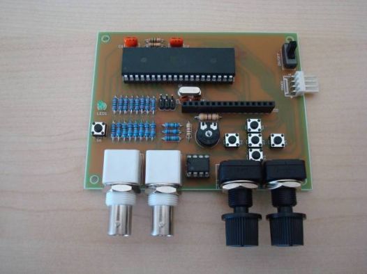
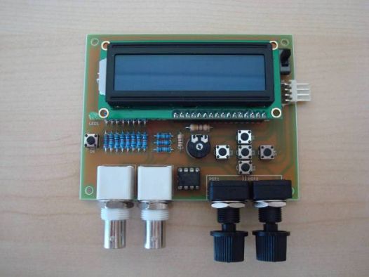
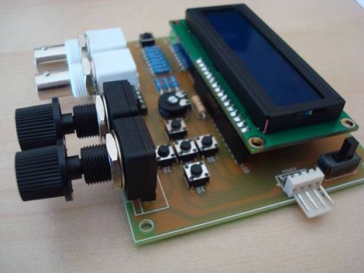
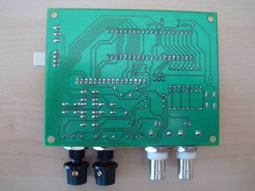
This is a new implementation of the AVR DDS signal generator v2.0, already published in scienceprog.com. It is obvious that full credit for the original schematic and the firmware goes to its original creator. Presented here is a different PCB that is compact, single sided with only through-hole components for easy construction.

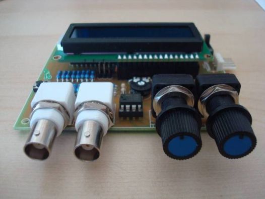
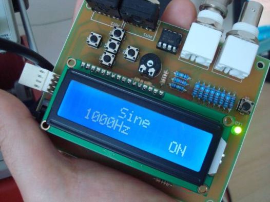
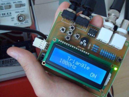
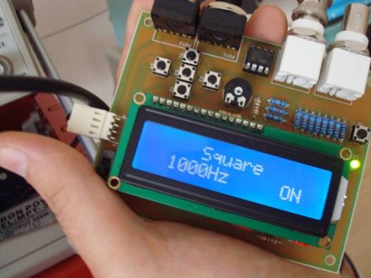
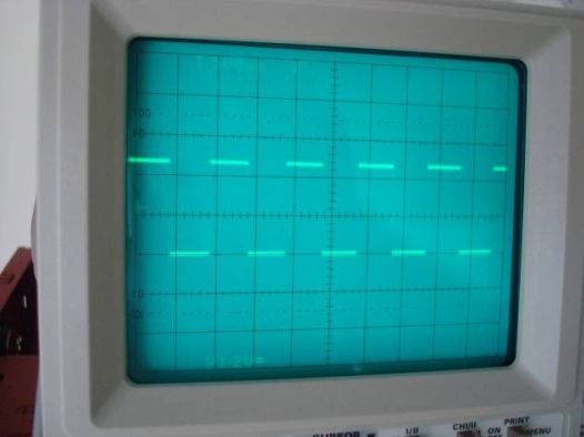
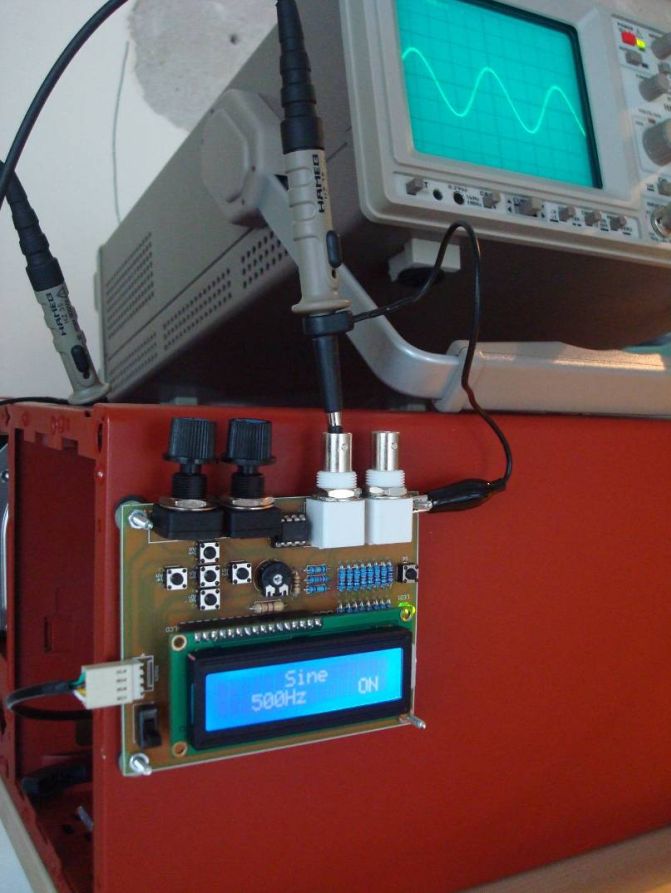
The function generator features two BNC outputs : one for the high speed [1 to 8 MHz] square signal (BNC1) and another for the DDS signal (BNC2). Offset and amplitude can be regulated by two potentiometers : offset in range of +5V to -5V (POT1) and amplitude in range of 0 to 10V (POT2). Up and down arrow buttons are used for changing the function type (sine, triangle etc.) while left and right arrow buttons are used for changing the frequency value. There is also a separate menu for changing frequency step. When the middle button is pressed, the signal generation starts. Middle button is pressed again for stopping the signal. More details can be found in the original site.

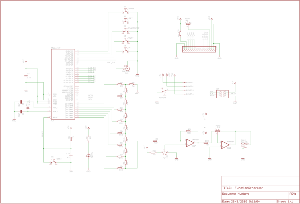
Schematic

Schematic

EAGLE Schematic (only a status led and an on/off switch was added)

Parts

Part Value
R1 470 Ω ½W 5%
R2 10 ΚΩ ¼W 5%
R3 100 ΚΩ ¼W 1%
R4 20 ΚΩ ¼W 1%
R5 20 ΚΩ ¼W 1%
R6 10 ΚΩ ¼W 1%
R7 20 ΚΩ ¼W 1%
R8 10 ΚΩ ¼W 1%
R9 20 ΚΩ ¼W 1%
R10 10 ΚΩ ¼W 1%
R11 20 ΚΩ ¼W 1%
R12 10 ΚΩ ¼W 1%
R13 20 ΚΩ ¼W 1%
R14 10 ΚΩ ¼W 1%
R15 20 ΚΩ ¼W 1%
R16 10 ΚΩ ¼W 1%
R17 20 ΚΩ ¼W 1%
R18 10 ΚΩ ¼W 1%
R19 20 ΚΩ ¼W 1%
R20 100 Ω ¼W 5%
R21 100 ΚΩ ¼W 1%
R22 12 ΚΩ ¼W 1%
R23 150 Ω ¼W 5%
POT1 1 ΚΩ linear potentiometer
POT2 47 KΩ linear potentiometer
POT3 10 ΚΩ trimmer
C1 100 nF MKT/polyester
C2 100 nF MKT/polyester
C3 18 pF ceramic
C4 18 pF ceramic
Q1 16 MHz crystal
IC1 ATMEL ATMEGA16P
IC2 LM358N
BNC1 – BNC2 BNC female connector
S1 – S6 Push button
LCD Header Female header 16 pin for LCD
LCD Module HD44780-based 2×16 character LCD
ISP Male header 2×3 for ISP
POWER Female header 4-pin for power as follows :
PIN1 : +12V
PIN2 : -12V
PIN3 : GND
PIN4 : +5V
LED1 3 mm green led
ON/OFF Miniature on/off switch

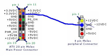
Power Supply

For powering up the function generator, a PC ATX power supply unit was used, where all voltages are already available (+12V, -12V, +5V). The wiring is shown in the following image, taken from scienceprog.com

molex_ATX

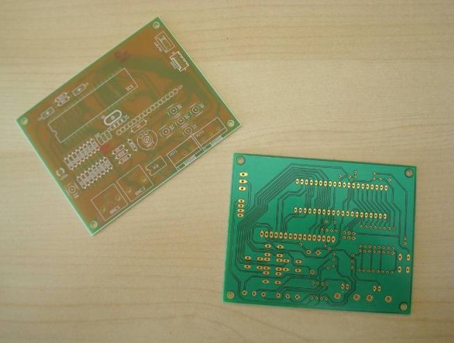
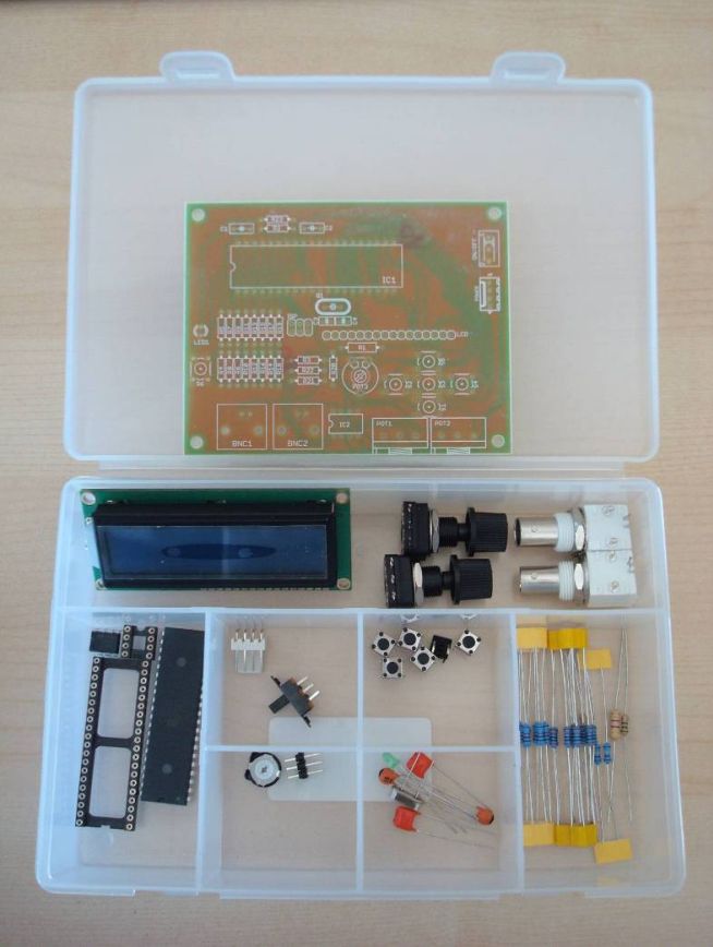
Photos of factory-made PCB and parts

Photo_1

Photo_2


Video

Photos of assembled PCB

Photo_3

Photo_4

Photo_5

Photo_6

Photo_7

Photo_8


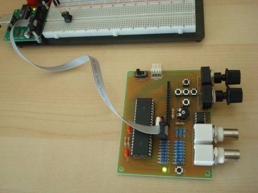
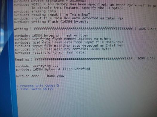
Programming of the ATMEGA16 with usbtiny programmer

Photo_9

Photo_10

The device firmware can be downloaded from :

http://www.scienceprog.com/avr-dds-signal-generator-v20

Changes in firmware

Because of the present LCD character orientation, which is different from the original implementation (180 degrees), the following changes in main.c were made :   

Buttons LEFT and RIGHT were reversed :
#define LEFT 3//PORTD
#define RIGHT 1//PORTD
Buttons TOP and BOTTOM were reversed :
#define DOWN 4//PORTD
#define UP 0//PORTD
For the latest version of AVR-GCC compiler, the following changes should be made (according to Geoff comment on scienceprog.com) :
struct signal{
volatile uint8_t mode; //signal
volatile uint8_t fr1; //Frequency [0..7]
volatile uint8_t fr2; //Frequency [8..15]
volatile uint8_t fr3; //Frequency [16..31]
volatile uint32_t freq; //frequency value
volatile uint8_t flag; //if 0 generator is OFF, 1 is ON
volatile uint32_t acc; //accumulator
volatile uint8_t ON;
volatile uint8_t HSfreq; //high speed frequency [1...4Mhz]
volatile uint32_t deltafreq; //frequency step value
}SG;
The ATMEGA16 fuses should be :
HIGH = 0×59
LOW = 0xCF
This is interpreted to the following options checked (all others unchecked) :
OCDEN
SPIEN
BOOTSZ1
BOOTSZ2
SUT1
SUT0

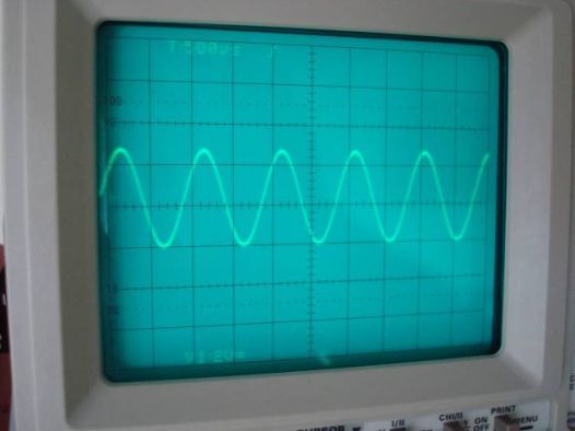
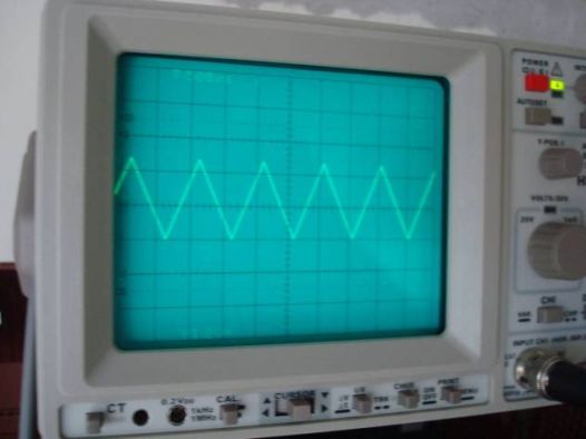
Photos of the device operation

Photo_11

Photo_12

Photo_13

Photo_14

Photo_15

Photo_16

Photo_17

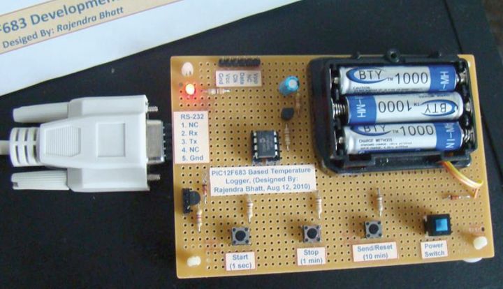
Single Chip Temperature Data Logger

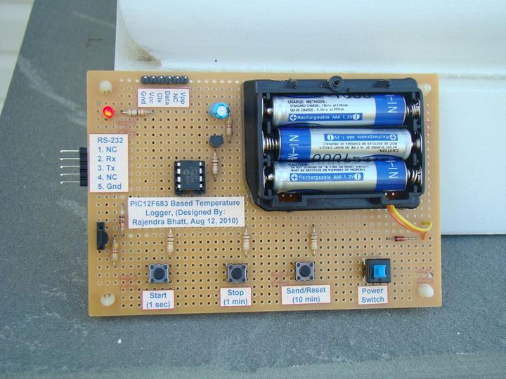
photo_1_th

Introduction

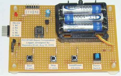
A data logger is a device that records measurements over time. The measurements could be any physical variable like temperature, pressure, voltage, humidity, etc. This project describes how to build a mini logger that records surrounding temperature values. It has following features:

  • Uses just one 8?pin chip, so very compact size circuit.
  • Temperature range: 0 to +125°C.
  • Can store up to 254 measurements.
  • Sampling interval options: 1 sec, 1 min, 10 min
  • Reset feature to clear all previous measurements.
  • Serial transfer of recorded measurements to a PC
  • Three tactile switches for user inputs and a LED indicator.

Description

The beauty of this project is that it uses just a single chip for logging. It is PIC12F683, an 8?pin microcontroller from Microchip. PIC12F683 has six general purpose I/O (GP0?GP5, GP3 is input only) pins, and 2K x 14 Flash program memorywith 256 bytes of internal EEPROM.

Temperature will be measured with a DS1820 temperature sensor. DS1820 is a one wire digital temperature sensor from Dallas Semiconductor (now MAXIM). The operating temperature range of the device is -55°C to +125°C with an accuracy of ±0.5°C over the range of -10°C to +85°C. The temperature sensor output is 9?bit Celsius temperature measurement, and so the temperature resolution corresponds to the least significant bit, and which is 0.5°C. But in this project we will use only the most significant eight bits. Therefore, the temperature resolution will be 1°C. The measured temperatures will be recorded into the internal EEPROM memory of PIC12F683.

The first location of the internal EEPROM will store the sampling interval of data logger. Sampling interval defines the time gap between two successive measurements. This project will have 3 options for sampling time: 1 sec, 1 min, and 10 min. These are user selectable. The second location of EEPROM will store the number of measurements recorded so far. And the remaining 254 EEPROM locations will store 8?bit temperatures. So, using 10 min sampling interval, 254 bytes of EEPROM will provide data logging for 42 hours. The recorded measurements can be sent to PC at any time through a serial link at 9600 baud.

photo_2

Transferring data to PC.

User Inputs

There will be three tact switches for user inputs, namely Start, Stop, and Send/Reset. The three switches will be able to accept the following 4 user requests.

  • Start: When ‘Start’ button is pressed, data logging starts.
  • Stop: Once the ‘Stop’ button is pressed, data recording will stop.
  • Send: Transfer data to PC through serial port.
  • Reset: Holding the ‘Send’ button for 2 sec or more clears the internal EEPROM memory.

Sampling Time Selection

The sampling interval can be selected as 1 sec, 1min, or 10 min using the same three switches. Suppose if we need 1 min sampling time, first turn OFF the power, then hold the ‘Stop’ button, turn the power ON, and wait till the LED glows. Once the LED glows, release the button, and the sampling interval will be set to 1 min. The new set sampling time will be updated to EEPROM location 0 so that in case of power failure, the previous sampling time will be restored. Similarly, use ‘Start’ and ‘Send’ buttons for 1 sec, and 10 min sampling intervals respectively.

LED Indicator

Every time the user presses input buttons, LED glows for a moment to indicate that the input is accepted. It also blinks thrice every time EEPROM Write operation takes place. It also blinks at the beginning when the power is turned ‘ON’. It also glows when the EEPROM memory is full.

Circuit Diagram

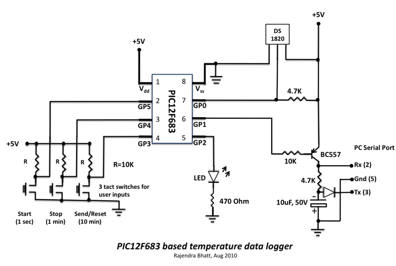
The complete circuit diagram for this project is shown below.

Schematic

List of Components

  • PIC12F683 microcontroller
  • DS1820 temperature sensor
  • BC557 NPN transistor
  • Resistors: 10K (4), 4.7K (2), 470 Ohm (1)
  • Capacitor: 10uF, 50V (1)
  • LED (1)
  • Tact switches (3)

Software

The firmware is written in C and compiled with mikroC compiler from MikroElektronika. I used the free version of it because our HEX output is going to be less than 2K. The download link for mikroC is http://www.mikroe.com/eng/downloads/get/29/mikroc_pro_pic_2010_v380_setup.zip

The 3 user input switches work on interrupt on change mode. That means any time the user presses any button, an interrupt is generated except at times when the microcontroller is reading temperature values from DS1820 (which is
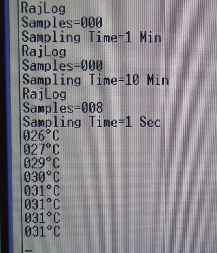
instantaneous) and when it is transferring data to a PC through serial port. The interrupts are disabled at those instants. The data transfer takes place at 9600 baud rate. You can write your own software to receive data on PC side, but I have used the Hyperterminal application for this purpose.

My Hyperterminal settings are bps : 9600, Data Bits: 8, Parity : None, Stop Bits : 1, Flow Control : Hardware

Hyperterminal receiving window

photo_3

Hyperterminal receiving window.

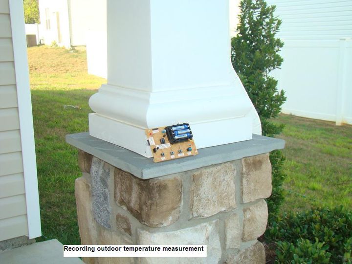
Photos

photo_4

photo_5

photo_6

Ultra High Sensitive Probe

Schematic

Description

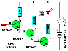
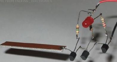
This circuit is so sensitive it will detect “mains hum.” Simply move it across any wall and it will detect where the mains cable is located. It has a gain of about 200 x 200 x 200 = 6,000,000 and will also detect static electricity and the presence of your hand without any direct contact. You will be amazed what it detects! There is static electricity EVERYWHERE! The input of this circuit is classified as very high impedance.

photo

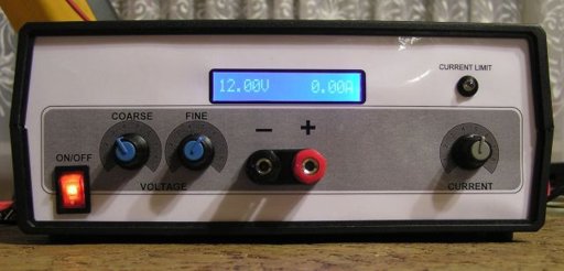
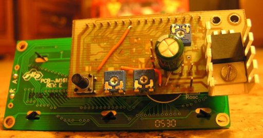
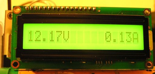
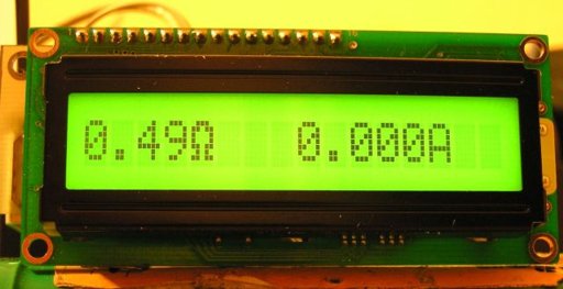
Voltmeter + Ammeter LCD panel

OLYMPUS DIGITAL CAMERA

Introduction

This multimeter was designed to measure output voltage and current in a PSU, where the current sense shunt resistor is connected in series with load at the negative voltage rail. It needs only one supply voltage that can be acquired from main PSU.

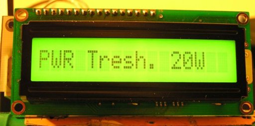
An additional function of the multimeter is that it can control (switch on and off) an electric fan used to cool the main heatsink. The power threshold at which the fan switches on can be adjusted using One Touch Button Setup.

Specifications

  • single uC ATMEL ATmega8 used to handle all the multimeter functions.
  • voltage range 0-30V.
  • voltage measure resolution 10mV.
  • current measure resolution 10mA (depended on current sense resistor value).
  • single, non isolated voltage supply.
  • one side PCB.
  • compact construction allowed to use the multimeter as panel meter.
  • compatibility with standard LCDs based on HD44780 controller.

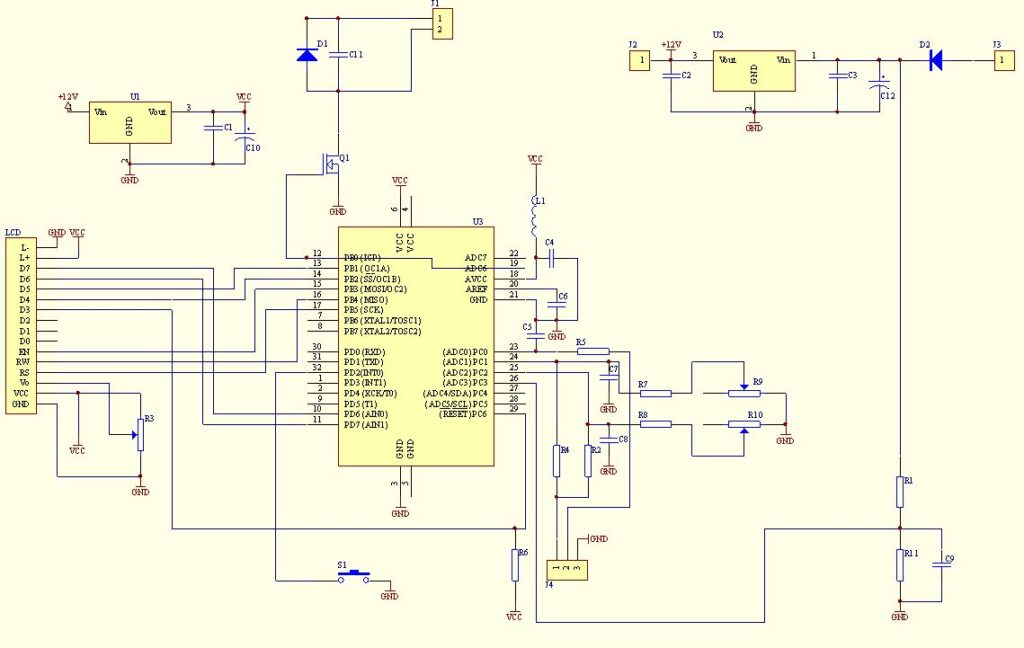
Schematic

Bellow you can see the multimeter schematic. There are some components in the parts list marked as “Do Not Assemble”. That components was needed in a previous software edition. Current software version doesn’t need them, so you just don’t add them. Maybe in a future version of the multimeter there will be a simpler PCB with simpler electronic diagram too.

schematic

PCB

PCB files are available on the download section below. There are two version of PCB – normal and mirrored. I think, that anyone who makes PCBs will know which one should be used to produce right PCB.

After soldering all the parts on PCB:

  • make two cross connection on PCB (see “Layout – bottom side”).
  • short L1 pads.
  • place U2 element (+12V voltage regulator) on heatsink .
  • pay attention on right polarity of D1 and D2 elements. Wider side of silk screen layout, where part number is placed, is CATHODE.

Parts

Element Value/Type Case Remarks
R1 100k 1206
R2 100k 1206
R3 10k Potentiometer
R4 30k 1206
R5 10k 1206
R6 10k 1206
R7 7k5 1206
R8 7k5 1206
R9 500R Potentiometer
R10 500R Potentiometer
R11 5k1 1206
C1 100n 1206
C2 100n 1206
C3 100n 1206
C4 100n 1206 Do Not Assemble
C5 100n 1206 Do Not Assemble
C6 100n 1206 Do Not Assemble
C7 100n 1206 Do Not Assemble
C8 100n 1206 Do Not Assemble
C9 100n 1206 Do Not Assemble
C10 22u/6V SMD A
C11 10n 1206 Optional element – protect Q1 against voltage peek after switch off fan. Most of the computer type fans which I tested didn’t produce  voltage peeks dangerous for Q1
C12 10u/50V
L1 47u 1210 Do Not Assemble – cross PCB pads
D1 DIODE SMD A Optional element – protect Q1 against voltage peek after switch off fan. Most of the computer type fans which I tested didn’t produce  voltage peeks dangerous for Q1
D2 DIODE SMD A e.g. SK310A
U1 7805 TO-252 Voltage regulator +5V, e.g. LM7805
U2 7812 TO220 Voltage regulator +12V, e.g. LM7812
U3 ATMEGA8 TQFP32
LCD GOLDPIN 1×16
J1 GOLDPIN 1×2 FAN_CON – fan connector
J2 GOLDPIN 1×1 +12V_CON – optional +12V supply connector
J3 GOLDPIN 1×1 +35V_CON  – main supply connector
J4 GOLDPIN 1×3 ground and measured signals
S1 SWITCH
Q1 MOSFET N SOT-23 e.g. BSS-138 (fan current lees than 200mA)

Programming

Because uC is in TQFP package, we can program it after soldering all components on PCB. After that, programming is quite easy to perform. Programming signals are delivered through LCD connector. To make the programming cable, you can use an old PC HDD cable. Picture of my programming cable is shown here:

OLYMPUS DIGITAL CAMERA

Remembered, that during programming, the circuit must be supplied with +5V. Depending on your programmer, supply voltage is provided either by programmer, or from separate power supply unit.

Programming cable connection list

LCD Pin number LCD signal uC signal/Pin Prog signal
1 GND GND GND
2 VCC VCC VCC
4 RS SCK / PB.5 SCK
5 RW MISO / PB.4 MISO
6 EN MOSI / PB.3  MOSI
10 D3 RESET RESET

After connecting uC to prog, you should check, if uC is “visible” for prog. When everything is fine, you can upload  code to uC. The code is available in the “Downloads” below .It is assumed that uC is new and works with its internal RC clock at 1MHz. If not, set appropriate fuse bits to achieve above mentioned conditions. In addition Brown-out detector should be turned on by enabling BODEN fuse. Recommended Brown-out Reset Threshold Voltage is 4V.

The next thing to do is to cross LCD soldering pads number 1 and 5. That’s necessary to provide ground for LCD RW signal. After all, connect LCD module with the multimeter PCB. It is recommended to use a detachable connector for further expandability e.g. software upgrading.

Installation in PSU and Regulation

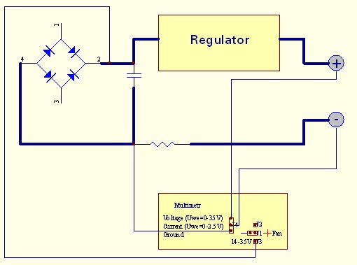
Mount multimeter to PSU according to the diagram below:

connection

Connectors and regulation elements

ELEMENT ACTION
S1 Setup button
When pushing this button the shunt resistor value appears. If the resistor value is known, repeat button pushing until correct value reached. If resistor value is unknown (e.g. self made resistor), short PSU output by ammeter, set some current by PSU current limit regulator and then, push button,  lead to equal current indication on ammeter and multimeter.After  resistor value setup, button must not be pressed for about 5 seconds. The next parameter to set up is fan switch-on power threshold. It is not the real power loosed on output transistor (transistors), because multimeter has information on voltage drop on transistor and driving current. To avoid instability switch-off threshold is automatically set to 20% less than switch-on one.
R9 Fine voltage circuit regulation potentiometer.
To reduce ADC conversion errors like un-linearity, gain factor etc. measuring range is divided into two sub-ranges 0-10V and 10-30V (switch threshold can be between 7-13V depend on sourcing current and elements tolerance).
To regulate fine sub-range connect voltmeter to PSU output, set up voltage at about 9V and turn R9 until voltmeter and multimeter indications are equal.
R10 Coarse voltage circuit regulation potentiometer..
There is over-sampling applied in multimeter software, so measuring resolution is the same in fine and coarse circuit and is 10mV. Because of the reason described above multimeter has two measuring circuits.
To regulate coarse sub-range connect voltmeter to PSU output, set up voltage at about 19V and turn R10 until voltmeter and multimeter indication are equal. (If  you posses 4.5 digit voltmeter, you could regulate at voltage 30V)
R3 LCD contrast potentiometer. Turn that potentiometer first, if nothing is visible on LCD.
J1 Fan connector.
Pin no. 1: Fan “+”
Pin no. 2: Fan “-“
J2 +12V
If +12V DC is available in your PSU, connect it to that pin. In that case you shouldn’t assemble +12V voltage regulator U2 on PCB.
That solution is convenient for multimeter, because eliminates U2 heating and permit to connect fan and LCD with higher current consumption.
If you haven’t got +12V DC in your PSU, left that pin unconnected.
J3 +35V
Rectifier bridge voltage. See U2 element you used data sheet to know about maximum voltage it can work properly. On the other hand the minimum voltage on that pin mustn’t drop bellow c.a. 9V, or 6.5V if low drop type U2 and U3 voltage regulators were used.
That pin should be connected even if +12V DC is connected to J2 pin. Voltage from that pin deliver information for fan switching.
J4 Measuring signal connector.
Multimeter is suitable for voltage and current measurement in PSU, where current sense shunt resistor is connected in series with load and is in negative rail.Pin no.1: voltage measurement U – connect to “+” PSU output, best directly to output terminal;Pin no.2: current measurement I – connect to “-” PSU output, best directly to output terminal;Pin no.3: ground – connect to shunt resistor terminal opposite to that connected to “-” PSU output.
LCD LCD connector.
Multimeter works properly with LCD’s 1×16 logical controlled as 2×8 (most of LCD’s available on the market).Because of linear voltage regulators used in multimeter, sourcing current is limited. Main current consumption elements are fan and LCD backlight, so:
– use LCD with LED backlight (typically current consumption is less than 15mA);
– use low speed, low current fan. Additional advantage of that solution will be silence.

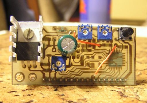
Photos

OLYMPUS DIGITAL CAMERA

OLYMPUS DIGITAL CAMERA

OLYMPUS DIGITAL CAMERA

OLYMPUS DIGITAL CAMERA

OLYMPUS DIGITAL CAMERA


Warnings

CAUTION
This circuit itself doesn’t work off the mains and there are not 220 VAC present, but PSU does.
Voltages above 50 V are DANGEROUS and could even be LETHAL.
In order to avoid accidents that could be fatal to you or members of your family please observe the following rules:

DO NOT work if you are tired or in a hurry, double check every thing before connecting your circuit to the mains and be ready to disconnect it if something looks wrong.
DO NOT touch any part of the circuit when it is under power.
DO NOT leave mains leads exposed. All mains leads should be well insulated.
DO NOT change the fuses with others of higher rating or replace them with wire or aluminium foil.
DO NOT work with wet hands.
If you are wearing a chain, necklace or anything that may be hanging and touch an exposed part of the circuit BE CAREFUL.
ALWAYS use a proper mains lead with the correct plug and earth your circuit properly.
If the case of your project is made of metal make sure that it is properly earthen.
If it is possible use a mains transformer with a 1:1 ratio to isolate your circuit from the mains.
When you are testing a circuit that works off the mains wear shoes with rubber soles, stand on dry non conductive floor and keep one hand in your pocket or behind your back.
If you take all the above precautions you are reducing the risks you are taking to a minimum and this way you are protecting yourself and those around you.
A carefully built and well insulated device does not constitute any danger for its user.

BEWARE: ELECTRICITY CAN KILL IF YOU ARE NOT CAREFUL

Simple Crystal Tester

schematic

Description

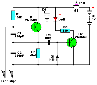
Transistor Q1, a 2N3563, and its associated components form an oscillator circuit that will oscillate if, and only if, a good crystal is connected to the test clips. The output from the oscillator is then rectified by the 1N4148 signal diode and filtered by C3, a 100pF capacitor. The positive voltage developed across the capacitor is applied to the base of Q2, another 2N3563, causing it to conduct.

When that happens, current flows through Led1, causing it to glow. Since only a good crystal will oscillate, a glowing LED indicates that the crystal is indeed OK. You can use the NTE123AP, PN100, or the 2N3904, for the transistors, however, the circuit works better with the 2N3563’s for crystals in the higher MHz. The NTE108 is a direct replacement for the 2N3563. R3, the 330 ohm resistor for the Led, can be lowered to 220/270 ohm if your application is for crystals in the high MHz, which makes the led glow dimly in some instances. The circuit is powered by a standard 9-volt battery and the SPST push button power-switch is included to prolong battery life but not really needed if you use a socket for the crystal-under-test. I’m using this particular simle tester myself.

Parts List

  • R1 = 100K C1,C2 = 220pF
  • R2 = 2K2 C3 = 100pF
  • R3 = 330 Ohm C4 = 0.1uF (100 nF)
  • Q1,Q2 = 2N3563 D2 = red led, ultra-bright
  • D1 = 1N4148 S1 = Momentary Push-button, SPST (optional)

Miscellaneous: crocodile clips (or others), 9V battery clip, wire, solder, etc

Transistor tester

photo_1

Description

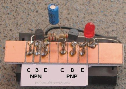
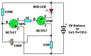
This is basically a high gain amplifier with feedback that causes the LED to flash at a rate determined by the 10u and 330k resistor. Remove one of the transistors and insert the unknown transistor. When it is NPN with the
pins as shown in the photo, the LED will flash. To turn the unit off, remove one of the transistors.

Schematic

schematic

This is basically a high gain amplifier with feedback that causes the LED to flash at a rate determined by the 10u and 330k resistor. Remove one of the transistors and insert the unknown transistor. When it is NPN with the
pins as shown in the photo, the LED will flash. To turn the unit off, remove one of the transistors.

Logic Probe Plus

logic probe plus -5

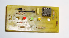
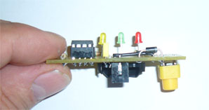
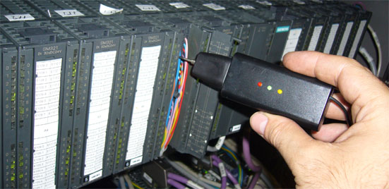
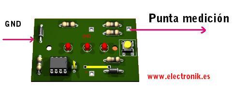
This project is based on a probe logic states, capable of measuring levels from TTL (5v) to state levels of PLC’s (24v). For this we have employed the use of the PIC 12F683 microcontroller, which by its nature is capable of operating at low voltages, in this case 3vcc, besides having analog inputs and internal oscillator.

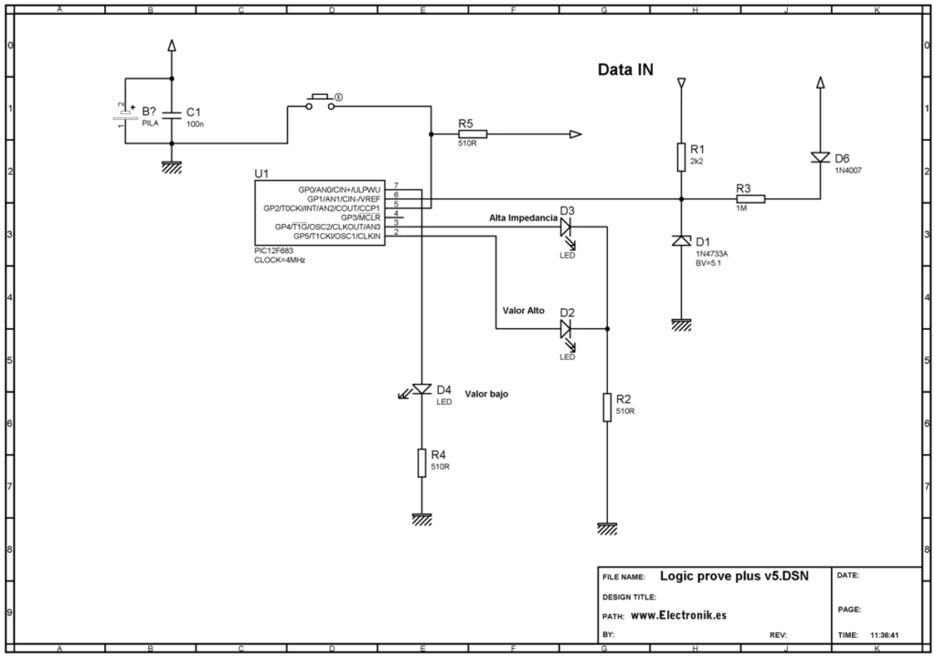
The circuit is supplemented by an input stage which will adapt the signal to the levels between the microprocessor is able to work and another output stage that will visually show the state in which the point is measured.

The input stage to include a voltage divider between R3 D5 and D1, their role is to establish a fixed value (/ – 2.80) for the input of the microcontroller which means that is in a state of high impedance, ie without input signal. When we apply the input signal DATA IN this will vary the voltage drop at point H so that the reading as we discriminate if this is higher or lower than the reference voltage.

The output stage is made up 3 LED (yellow = high impedance, Green = Red = logic 1 and logic 0).

logic probe plus -1

logic probe plus -3

logic probe plus -2

The program also has an internal timer to approximately 3 minutes between the microcontroller in sleep mode in which consumption will be minimal, to save the battery. And it will reactivate the program until you press the button, starting over allowing timing and take readings we require.

logic probe plus -4

Focusing on the program of the microprocessor, this is configured to work with internal oscillation 4Mhz and configuring its pin so that analog reading take from point H by the GP1 pin, which is defined for a resolution of 10 bits, pin GP2 will also be defined as input and will be connected through a resistor (PULL UP) and a secondary switch to ground, which will be responsible for collecting the press that forced the interruption level change in GP2 While the interruption occurs loads a value (2000) as a timer to make a loop past work and this time will be placed the microcontroller in sleep mode.

esquema

The program is also complimented inizialización a function which shows the blinking leds, to argue that this in active process and that at the end of this sequence we can take appropriate measures.

The bulk of the program is effected by a loop of reading and comparing the reading which collects and compares GP1 activating the corresponding output.

In order to function alone is sufficient to connect the ground wire to any metal part of the chassis or failing to ground.

conexion

The code is open and available to anyone who want, just send an e-mail and ask.

Logic Probe

Logic Probe

Description

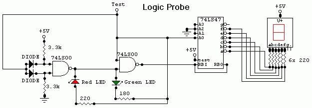
This circuit is a Logic Probe. It indicates the logic state of the node of any TTL logic circuit. To do that, we have to supply the probe with the same power of the circuit that we want to analyse: same Vcc and same GND. To check the logic level, we must connect the “Test” wire of the probe to the desired node of the circuit that we want to check.

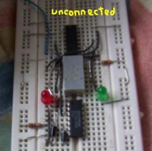
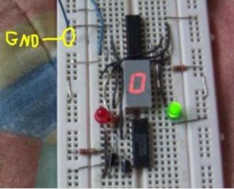
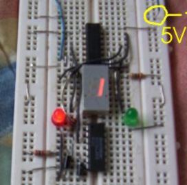
If the level is Low, the probe will display a “zero” (0) and only the green LED will be lighted. If the level is High, the probe will display a “one” (1) and only the red LED will be lighted. If the level is Impedance, the probe will display a nothing and no LED will be lighted. The logic level is “Low” when the “Test” wire is connected to the ground of the circuit (the voltage is between 0V and 2V). The logic level is “Impedance” when the “Test” wire is unconnected (it has no voltage or the voltage is between 2V and 3V). The logic level is “High” when the “Test” wire is connected to the positive supply of the circuit (the voltage is between 3V and 5V).

Photos

Impedance

Low

High

Led display digital Voltmeter

image_2

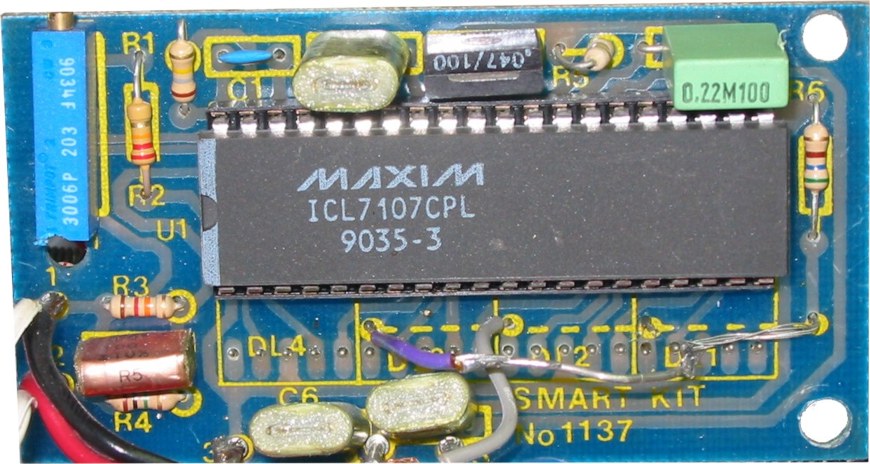
Copyright of this circuit belongs to Smart kit electronics. On this page, we will use this circuit to discuss improvements and we will introduce some changes based on the original schematic.

General Description

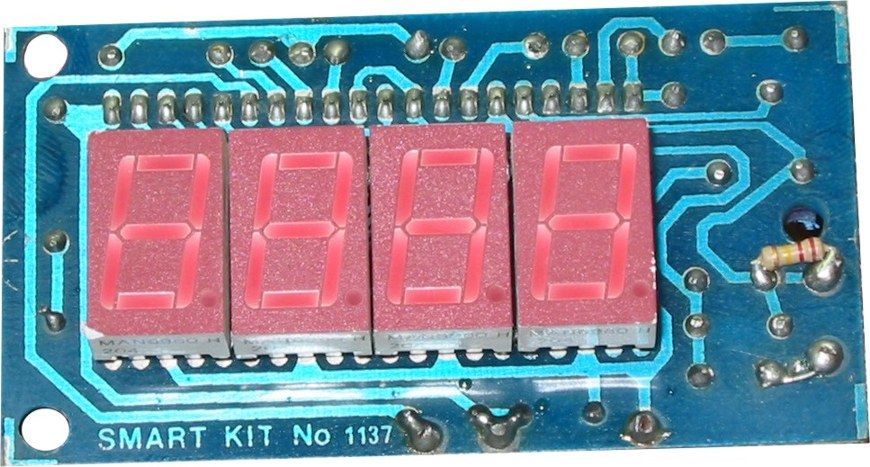
This is easy to build, but nevertheless very accurate and useful digital voltmeter. It has been designed as a panel meter and can be used in DC power supplies or anywhere else it is necessary to have an accurate indication of the voltage present. The circuit employs the ADC (Analogue to Digital Converter) I.C. CL7107 made by INTERSIL. This IC incorporates in a 40 pin case all the circuitry necessary to convert an analog signal to digital and can drive a series of four seven-segment LED displays directly. The circuits built into the IC are an analog to digital converter, a comparator, a clock, a decoder, and a seven-segment LED display driver. The circuit as it is described here can display any DC voltage in the range of 0-1999 Volts.

Technical Specifications – Characteristics

  • Supply Voltage: …………. +/- 5 V (Symmetrical)
  • Power requirements: ….. 200 mA (maximum)
  • Measuring range: ………. +/- 0-1,999 VDC in four ranges
  • Accuracy: ………………….. 0.1 %

Features

  • Small size
  • Easy construction
  • Low cost.
  • Simple adjustment.
  • Easy to read from a distance.
  • Few external components.

How it Works

In order to understand the principle of operation of the circuit, it is necessary to explain how the ADC IC works. This IC has the following very important features:

  • Great accuracy.
  • It is not affected by noise.
  • No need for a sample and hold circuit.
  • It has a built-in clock.
  • It has no need for high accuracy external components.

schematic

7seg

An Analogue to Digital Converter, (ADC from now on) is better known as a dual-slope converter or integrating converter. This type of converter is generally preferred over other types as it offers accuracy, simplicity in design, and relative indifference to noise which makes it very reliable. The operation of the circuit is better understood if it is described in two stages. During the first stage and for a given period the input voltage is integrated, and in the output of the integrator at the end of this period, there is a voltage that is directly proportional to the input voltage. At the end of the preset period, the integrator is fed with an internal reference voltage and the output of the circuit is gradually reduced until it reaches the level of the zero reference voltage. This second phase is known as the negative slope period and its duration depends on the output of the integrator in the first period. As the duration of the first operation is fixed and the length of the second is variable it is possible to compare the two this way the input voltage is in fact compared to the internal reference voltage and the result is coded and is sent to the display.

image_3

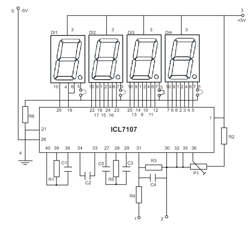
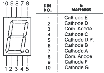
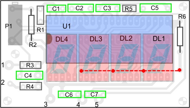
All this sounds quite easy but it is in fact a series of very complex operations which are all made by the ADC IC with the help of a few external components which are used to configure the circuit for the job. In detail the circuit works as follows. The voltage to be measured is applied across points 1 and 2 of the circuit and through the circuit R3, R4 and C4 is finally applied to pins 30 and 31 of the IC. These are the input of the IC as you can see from its diagram. (IN HIGH & IN LOW respectively). The resistor R1 together with C1 are used to set the frequency of the internal oscillator (clock) which is set at about 48 Hz. At this clock rate there are about three different readings per second. The capacitor C2 which is connected between pins 33 and 34 of the IC has been selected to compensate for the error caused by the internal reference voltage and also keeps the display steady.  The capacitor C3 and the resistor R5 are together the circuit that does the integration of the input voltage and at the same time prevent any division of the input voltage making the circuit faster and more reliable as the possibility of error is greatly reduced. The capacitor C5 forces the instrument to display zero when there is no voltage at its input. The resistor R2 together with P1 are used to adjust the instrument during set-up so that it displays zero when the input is zero. The resistor R6 controls the current that is allowed to flow through the displays so that there is sufficient brightness with out damaging them. The IC as we have already mentioned above is capable to drive four common anode LED displays.  The three rightmost displays are connected so that they can display all the numbers from 0 to 9 while the first from the left can only display the number 1 and when the voltage is negative the «-« sign. The whole circuit operates from a symmetrical ρ 5 VDC supply which is applied at pins 1 (+5 V), 21 (0 V) and 26 (-5 V) of the IC.

Parts List

R1 = 180k
R2 = 22k
R3 = 12k
R4 = 1M
R5 = 470k
R6 = 560 Ohm

C1 = 100pF
C2, C6, C7 = 100nF
C3 = 47nF
C4 = 10nF
C5 = 220nF

P1 = 20k trimmer multi turn

U1 = ICL 7107

LD1,2,3,4 = MAN 6960 common anode led displays

0-20 V ….R3 = 1.2K
0-200 V …R3 = 12K
0-2000 V ..R3 = 120K


Construction

First of all let us consider a few basics in building electronic circuits on a printed circuit board. The board is made of a thin insulating material clad with a thin layer of conductive copper that is shaped in such a way as to form the necessary conductors between the various components of the circuit. The use of a properly designed printed circuit board is very desirable as it speeds construction up considerably and reduces the possibility of making errors.  To protect the board during storage from oxidation and assure it gets to you in perfect condition the copper is tinned during manufacturing and covered with a special varnish that protects it from getting oxidised and also makes soldering easier.

Soldering the components to the board is the only way to build your circuit and from the way you do it depends greatly your success or failure. This work is not very difficult and if you stick to a few rules you should have no problems. The soldering iron that you use must be light and its power should not exceed the 25 Watts. The tip should be fine and must be kept clean at all times. For this purpose come very handy specially made sponges that are kept wet and from time to time you can wipe the hot tip on them to remove all the residues that tend to accumulate on it.
DO NOT file or sandpaper a dirty or worn out tip. If the tip cannot be cleaned, replace it. There are many different types of solder in the market and you should choose a good quality one that contains the necessary flux in its core, to assure a perfect joint every time.
DO NOT use soldering flux apart from that which is already included in your solder. Too much flux can cause many problems and is one of the main causes of circuit malfunction. If nevertheless you have to use extra flux, as it is the case when you have to tin copper wires, clean it very thoroughly after you finish your work.
In order to solder a component correctly you should do the following:

  • Clean the component leads with a small piece of emery paper.
  • Bend them at the correct distance from the component’s body and insert the component in its place on the board.
  • You may find sometimes a component with heavier gauge leads than usual, that are too thick to enter in the holes of the p.c. board. In this case use a mini drill to enlarge the holes slightly.
  • Do not make the holes too large as this is going to make soldering difficult afterwards.

layout_full

Mosfet Tester

schematic


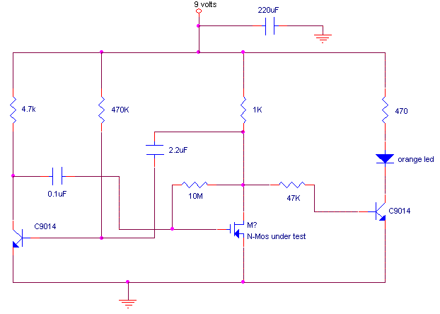
This is a variation on the astable multivibrator. Circuit was recently developed to test for N-mosfets (the power kind e.g irf830)

I don’t claim circuit can test all bad mosfets or all fault mosfet conditions. If mosfet is working it will operate in the astable multivibrator circuit causing the Led to flash.

A bad mosfet will not cause the LED to flash.

Below is the circuit diagram,  the other half of the astable utilizes an npn transistor to make the circuit cheap.

Almost any npn transistor will work in this circuit.

The npn transistor to the right is used as a common emitter buffer that also drives the led as it receives pulses from the mosfet drain.

Note diode is a light emitting Diode

TOP PCB Companies