0-30V Laboratory Power Supply

DSC_0005

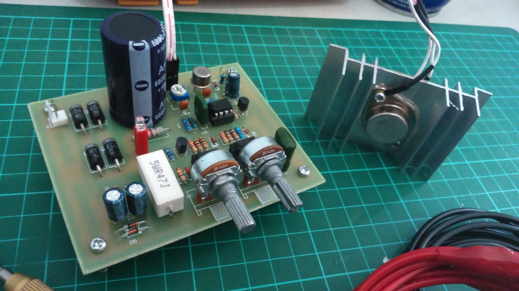
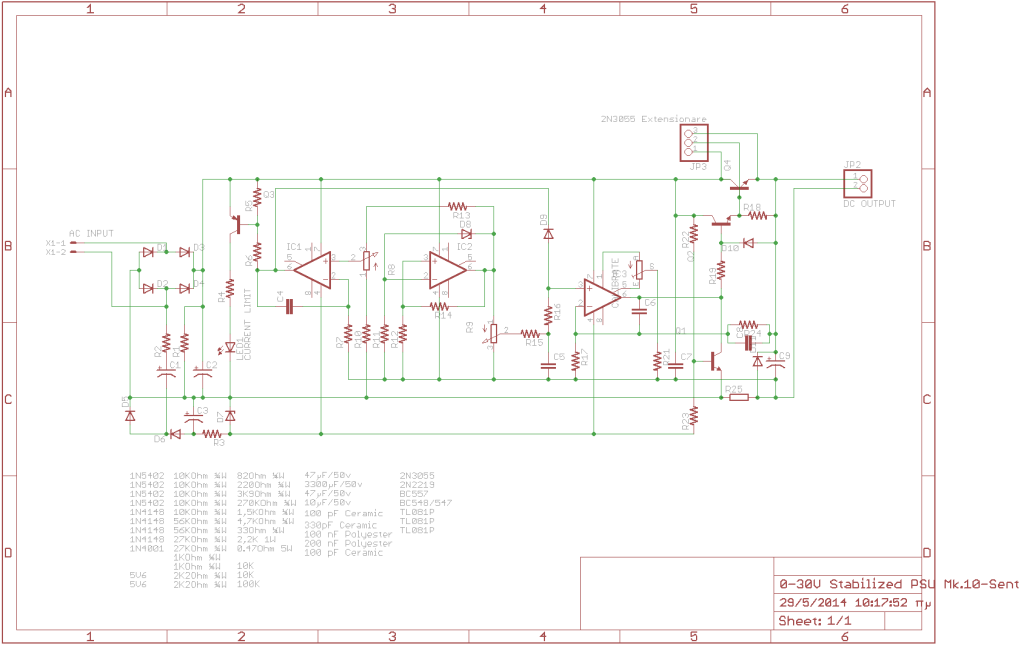
This project is based on the 0-30 VDC Stabilized Power Supply with Current Control 0.002-3 A and a new PCB layout is introduced here. It’s a stabilized power supply with variable output voltage in the range 0-30Vdc (33Vdc peak) – and variable current 3A and is ideal for your laboratory power supply.

Description

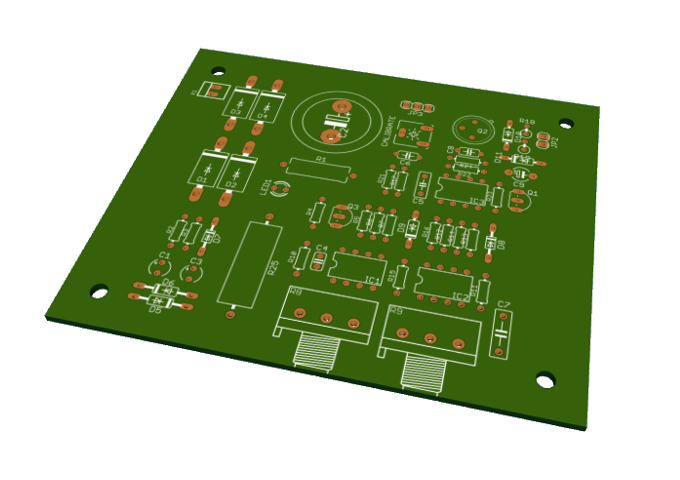
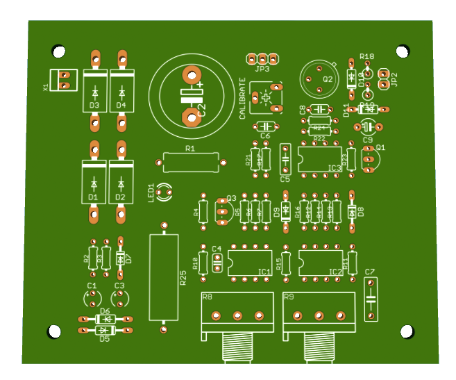
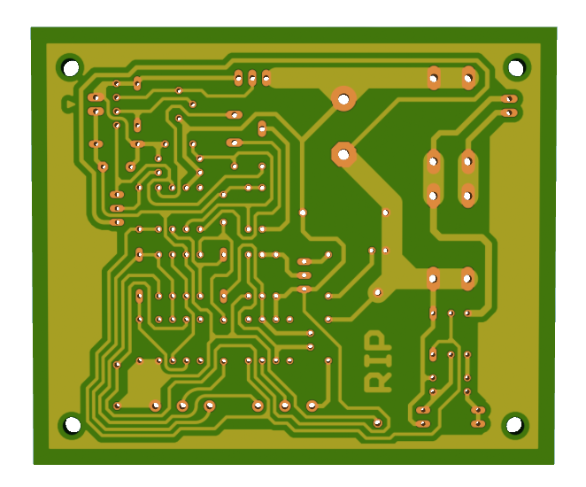
Schematic and PCB are designed in Eagle software and the source files are available on the links at the bottom of the page. The PCB design has connectors for 2N3055 transistor, input and output voltage. Also on-board potentiometers are added.

Schematic

schematic

Photos

3D_pcb_top_first

3D_pcb_top

3D_pcb_top_bottom

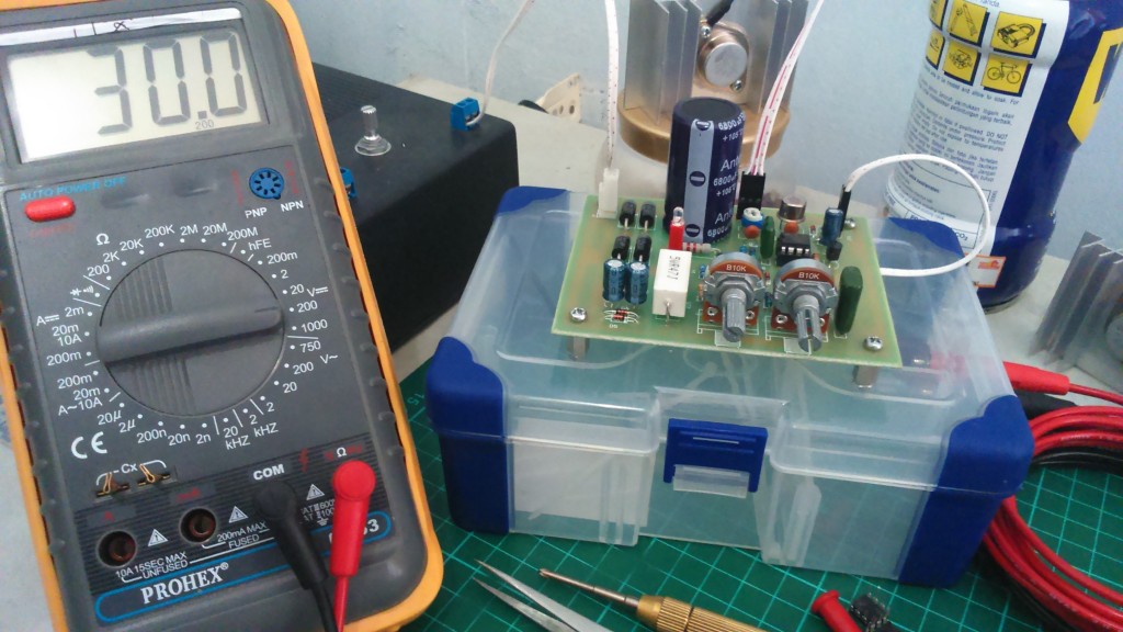
DSC_0009

Variable Power Supply with LM7812

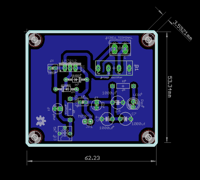
pcb_regulator_main

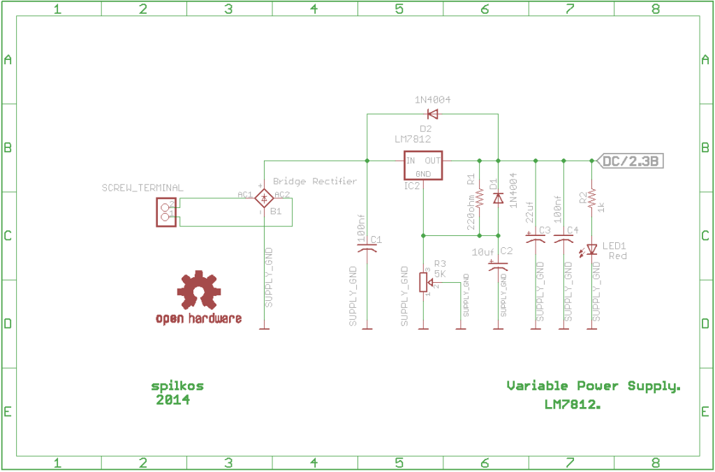
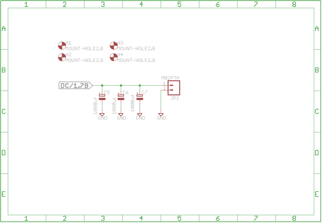
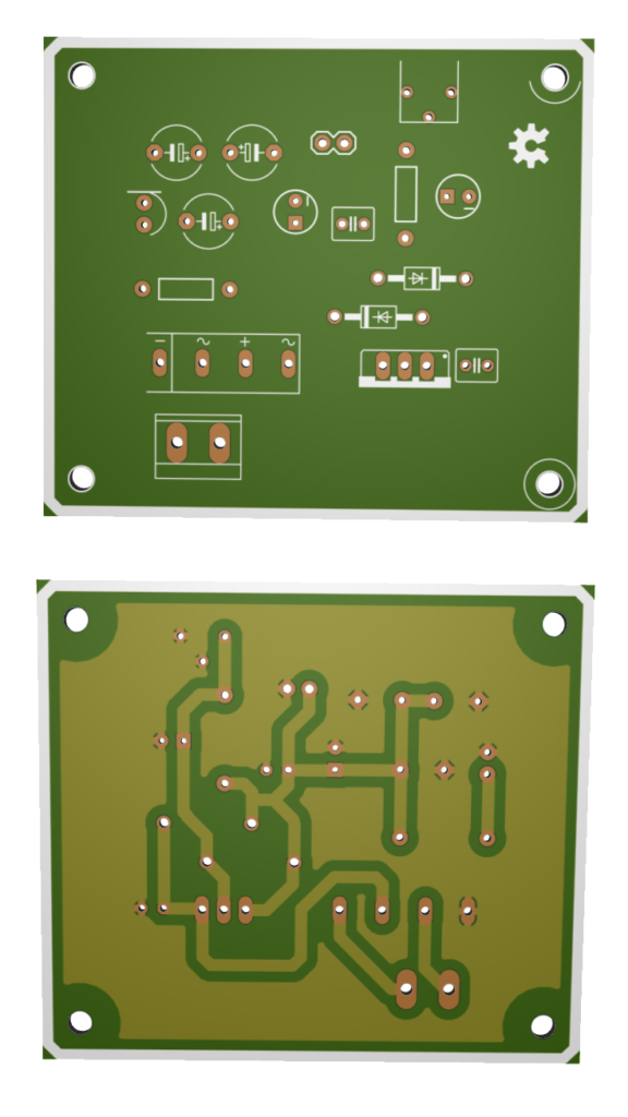
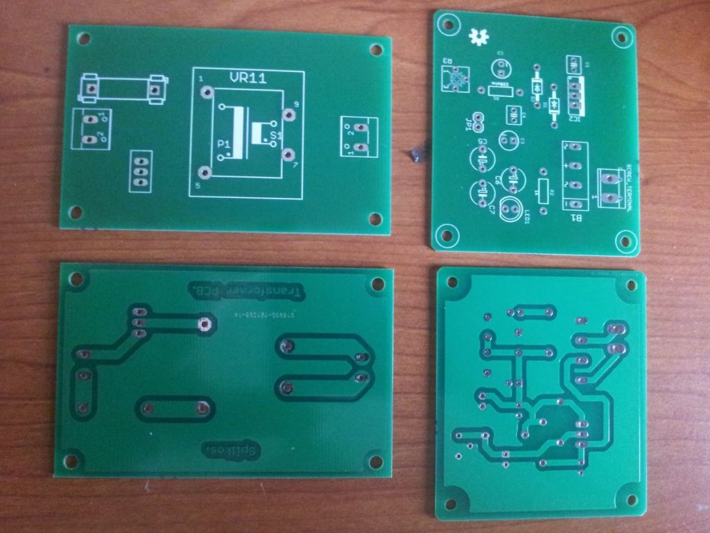
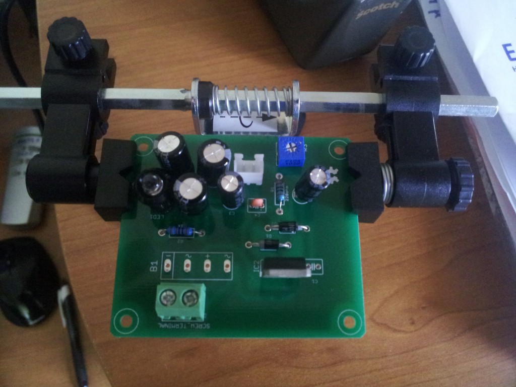
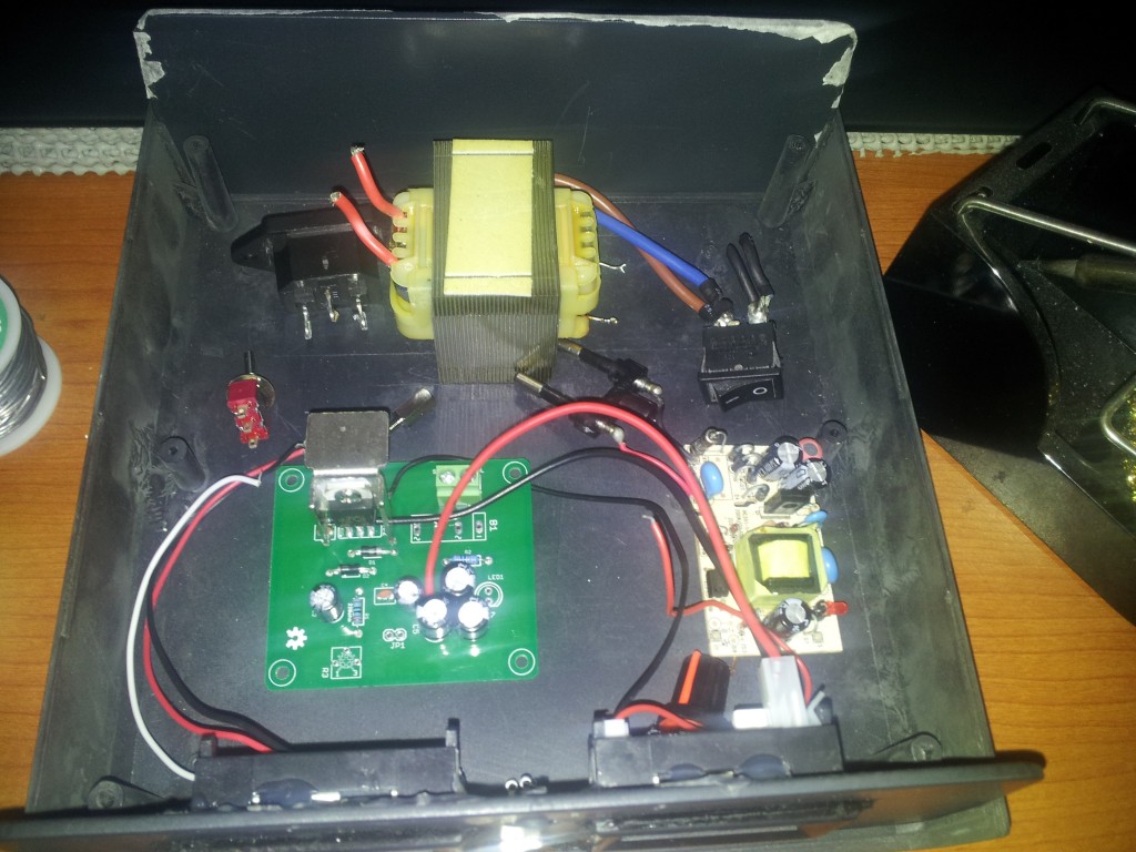
This project is a simple variable power supply using the famous LM7812 regulator IC. It consists of two boards, the main board which includes the regulator, capacitors, bridge rectifier and potentiometer and a second board that includes the mains tranformer, the fuse and a switch.

Description

I designed this variable power supply which is based on the famous series of voltage regulator LM78xx. The electrical characteristics can be found here. LM78xx can be easily found in stores with electronic materials.

On this project I use the LM7812 in TO-220 footprint, which can be screwed to the rear of a heatsink for better heat dissipation. You will get better heat conduction if you use thermal paste between the heatsink and LM78xx before screwed together.

The bridge rectifier is a classic 2KVV. You may choose the appropriate bridge rectifier according to your requirements.

The variable resistor R3 varies the output voltage (Vout). The R3 can be placed in your project box and can be replaced with a potentiometer of similar price.

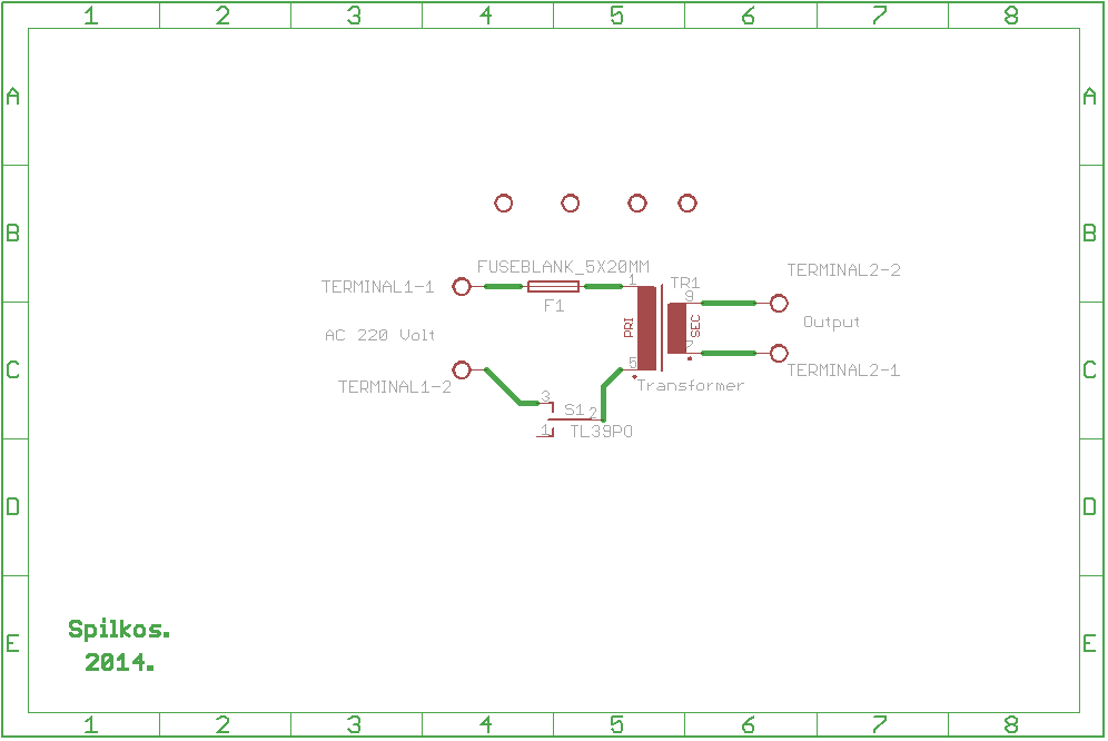
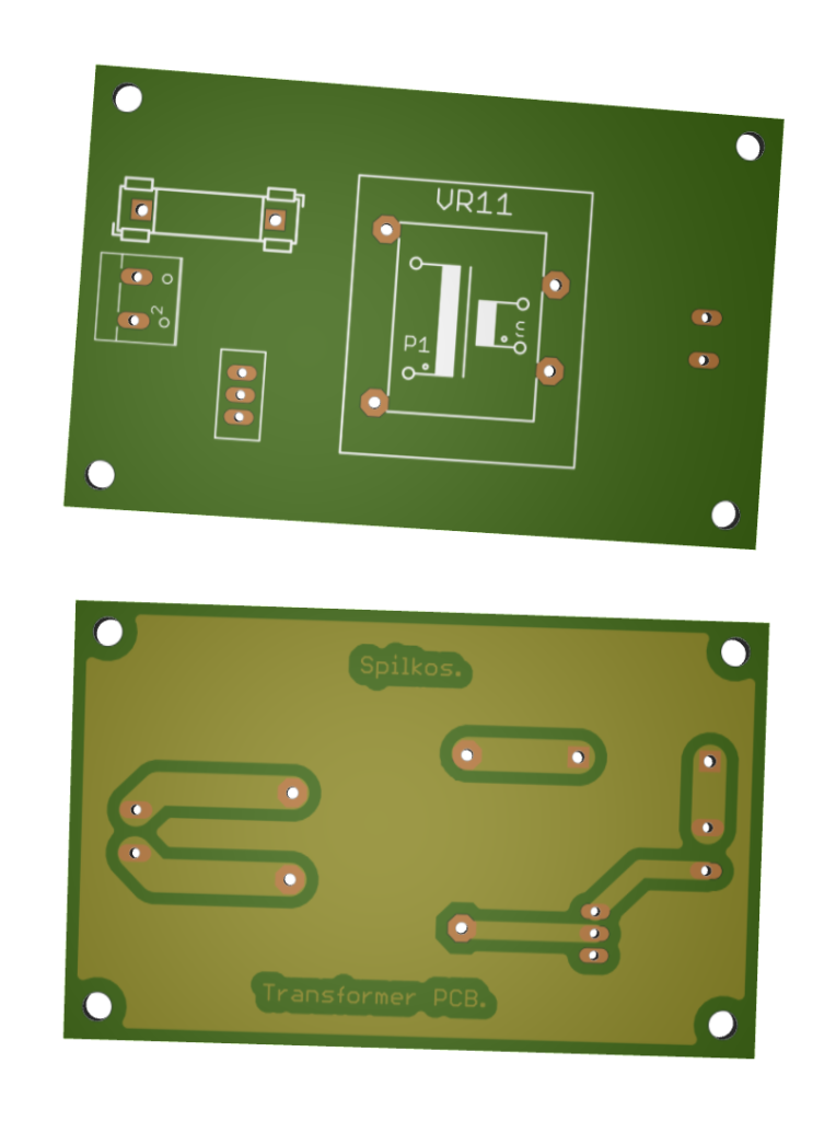
The second board is for the transformer, the board contains the base for the primary fuse and one on-off switch for 220V mains voltage.

Schematics

Regulator board

schematic_1

schematic_2

Transformer board

schematic_3

Photos

3D_pcb_regualtor

3D_pcb_tranformer

pcb_photo

Power Supply_1

Power Supply_2

Power Supply_3

MCU Controlled Spot Welder

3d_pcb_1_th

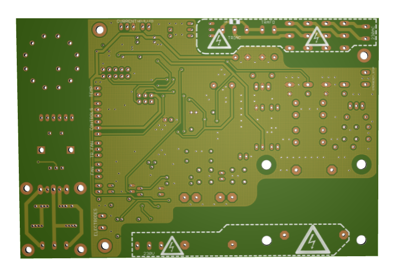
This project is a controller for a dual pulse spot welder that has some nice features that are controlled using a LCD interface.

Description

I always wanted a spot welder, so I decided to built one. I wanted to build a capacitance discharge one but I couldn’t afford for the capacitors at this time. So this is a controller for a dual pulse spot welder with some few extras:

  • It has a zero cross detector. You could power the transformer at zero cross or dim the transformer if you like
  • The transformer is triac controlled
  • It has an hd44780 interface
  • An spi interface for single thermocouple
  • Peak detector of a current transformer
  • Isolated foot switch
  • Voltage monitor with opmaps
  • An attempt to sense when the user tries to weld
  • Single rotary switch for operation and single rotary encoder for setting up

I have used an Atmega328P and I will probably write the code in arduino IDE.
You could probably use the pcb for other applications, like:

  • Ac dimmer
  • Simple thermostat, or
  • PID thermostat with dimming output

Further update on the project after the delivery on the pcbs.

Schematics
power_supply_sch

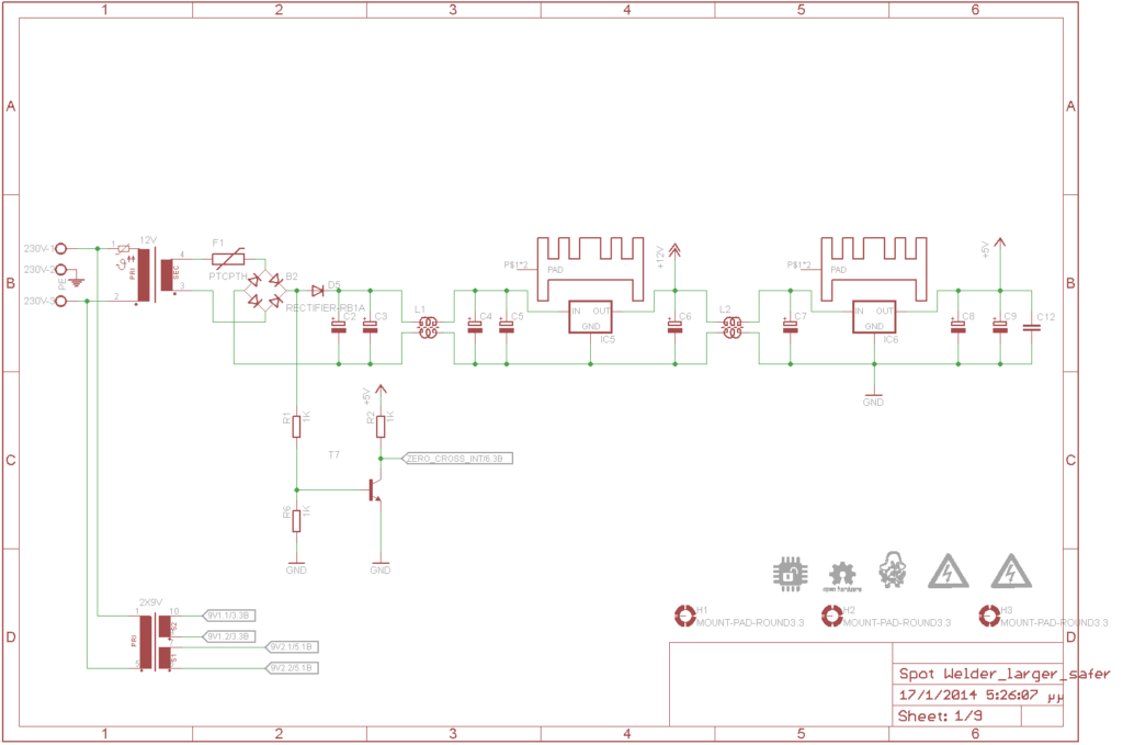
The main power supply for the controller. The main transformer is 1x12VAC 1Amp (TR-15)
The PTC fuse is 0.9A with a 2W10 bridge rectifier and a 1n4007 diode, smoothing capacitors, common mode choke to remove any spikes and unwanted noise, some more capacitors, linear voltage regulator 7812 with heatsink, more caps, more chokes, more caps again, 7805 and 5v rail.
The T7 is a 2n3904 npn transistor that senses both of the AC zero crosses for the dimming circuit.
The other transformer is a 2x9Vac 0.1Amp for the secondary isolated circuits.

Power OK
power_ok_sch

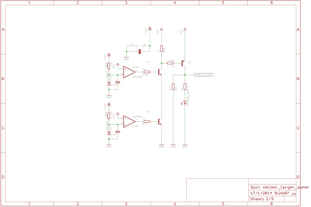
I had some space I thought to make a voltage supervisor of the 5V rail.
The two opAmps works as comparators for the 5V rail. The first IC3A checks if the voltage on the non inverting input is lower than the zener voltage (5.3V), if so the output of the opAmp is set High (12V) and T4 is turning on.
The IC3B checks if the voltage is higher than the zener voltage ( 4.7V), if so the output of the opAmp is set High (12V) and T5 is turning on.
Now if both transistors are ON then Q1 turning on and powering the led and setting the PWR_OK signal high.

Foot Switch
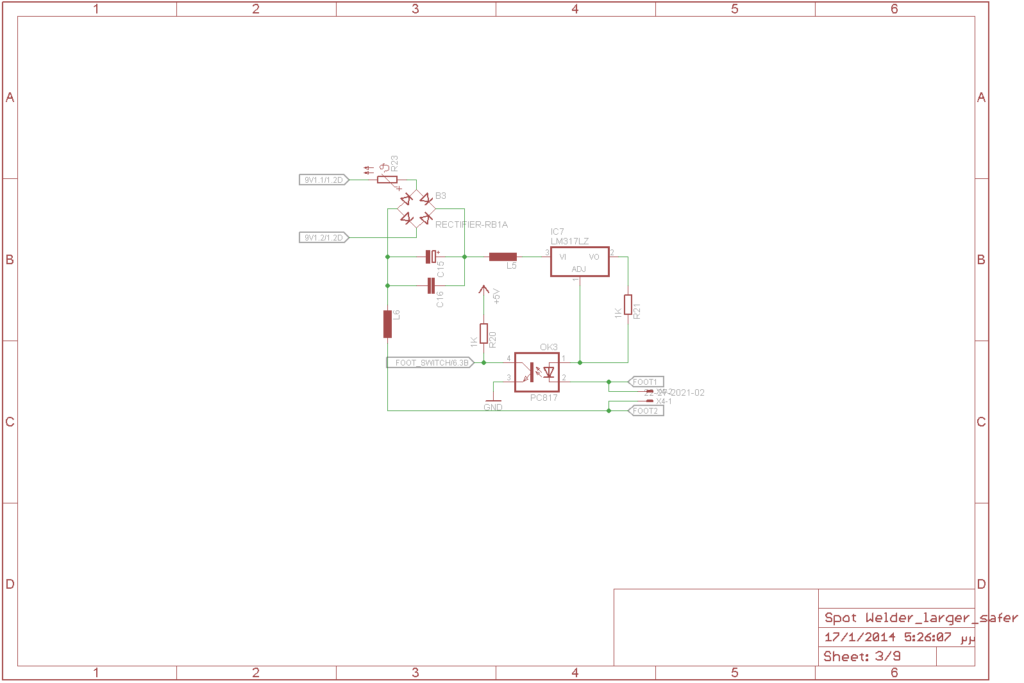
foot_pedal_sch

This is an opto-Isolated switch input to the uC. 9V comes in from the transformer, B3 is also an 2W10 bridge rectifier with some smoothing capacitors and two in series inductors powering a LM317 (TO-92) working as a constant current driver for the opotcoupler led. If you close the switch the led turns on and the signal FOOT SWITCH goes low.

Current Measure
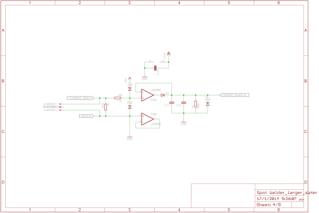
current_measure_sch

This circuit connects to a current transformer and measures the peak current of the weld. The current waveform is feeding to the non inverting input of IC8A, the two zener diodes protect the input of the opAmp from voltages lower than 0V and higher than 5V. D1 is only allowing the opamp to charge the capacitors at the peak voltage of the current transformer and zener diode protects the input of the uC.

Electrodes Touch
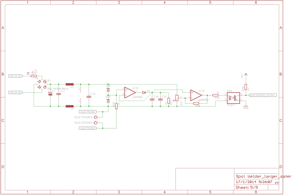
electrode_state_sch

This circuit is an to attempt to automate the spot welder. The idea is to sense when the user places the electrodes on the battery and after a short delay and a buzz to power the transformer. But I think is going to fail. I am going to try to power the weld transformer a little bit before the zero cross.

If the current is zero then the user is not trying to weld or if the voltage across the the two leads is higher that a limit then the user is not trying to weld ( the electrodes are not shorted ).

The same isolated power supply as before and the same peak detector but this time the output of the peak detector is feeding two a second opAmp working a comparator. If the output of the peak detector on the non inverting input of the opAmp is lower than the set voltage on the inverting input from the 10-turn pot the output of the opamp is high, the led turns on and the  signal ELECTRODES_TOUCH goes low.

uC
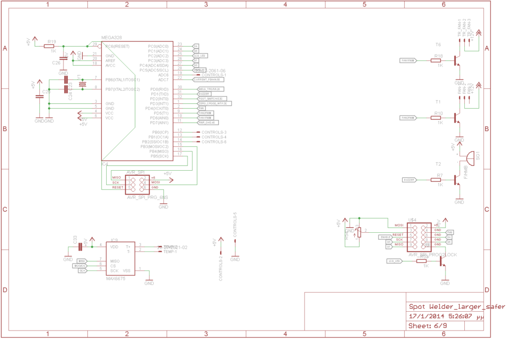
mcu_sch

The uC is an AtMega328 in tqfp32 package running at 16Mhz and the code will be written in Arduino IDE There is an spi thermocouple interface MAX6675 for the weld transformer, two PWM controlled fan headers, a buzzer and U$4 is for the LCD with Hitachi HD44780 controller.

Switch
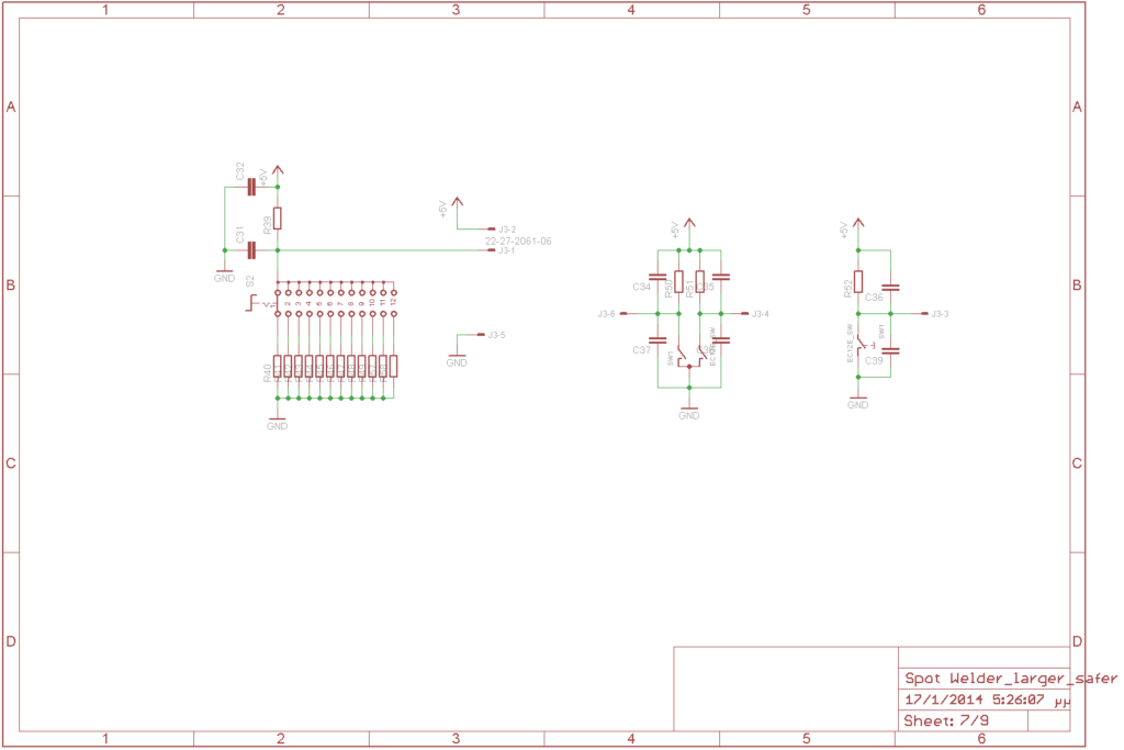
switch_sch

The interface with the user is pretty simple. There is 12 position rotary switch for the 12 preset modes of operation and a rotary encoder with a push button for navigating in the menu and setting the preset modes of operation.

Weld transformer controll
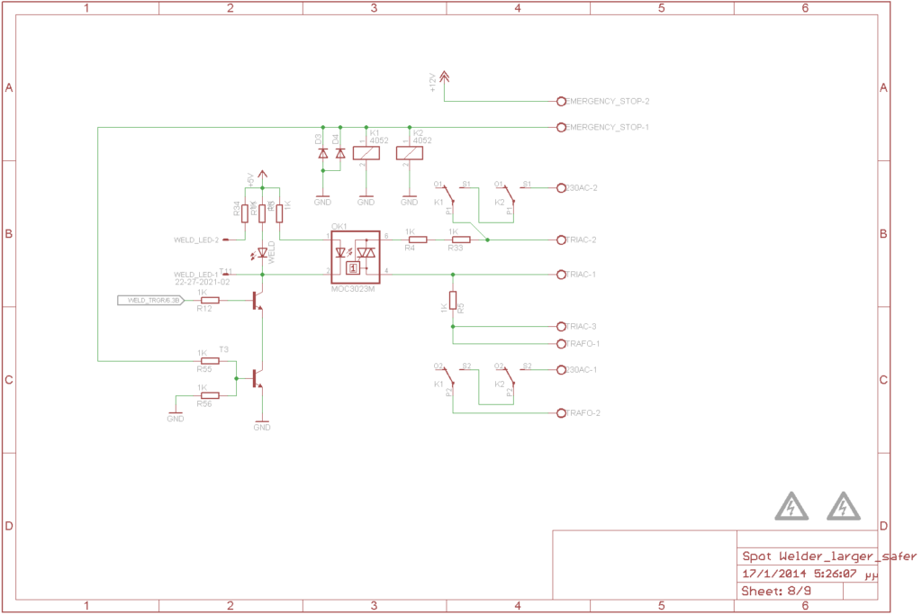
trafo_control_sch

K1 and K2 are two 12Vdc coil relays with dual pole dual throw contacts. Live and natural line are passing through the contacts of both of the relays and the  relays coils are triggered by the normaly closed emergency stop button, as well as the led on the opto-triac needs the 12V  from the emergency stop button. Also there is a led that switch on when the opto-triac switch on and a pin header for a led closer to the transformer.

Snubbers
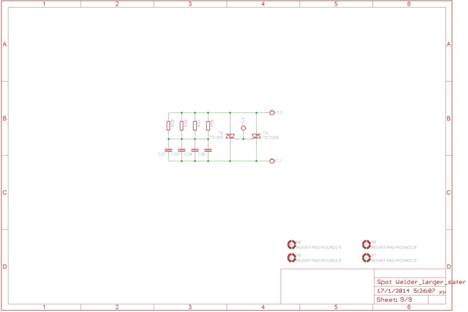
snubber_sch_th

Just a separate pcb for the RC snubber circuit with multiple pads for various packages of  resistors, capacitors and triacs.

Photos
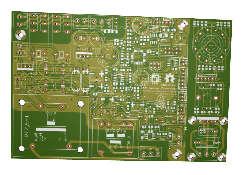
3d_pcb_1

3d_pcb_2

3D PCB renderings

Digital Multiple Voltage Power Supply

MC_ Power_Supply_3D_Sideview_th

1.2 to 33 Volts DC @ 3 Amps

Description

This is simple to build microcontroller controlled power supply that can switch between 5 (or 32 or more) preconfigured voltages between 1.2 to 33 volts dc and up to 3 amps. This guide will walk you through every aspect of the building process; however some basic familiarity with electronics and microcontrollers will be required to program the microcontroller.

Specifications

  • Input Voltage: 33 Volts DC* Max
  • Input Current: 3 Amps Max
  • Output Voltage: 5 Preset Voltages Between 1.2 to 33** Volts DC
  • Output Current: 3 Amps Max

*There is no bridge rectifier so the input voltage must be DC.
**Output voltage won’t exceed input voltage.

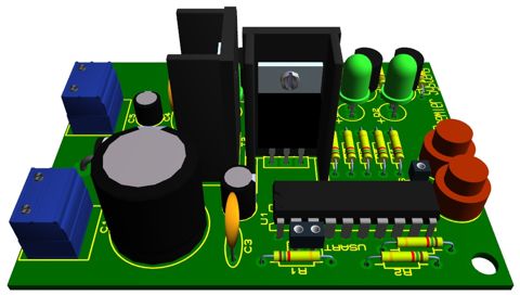
MCU_Power_Supply_3D

Description

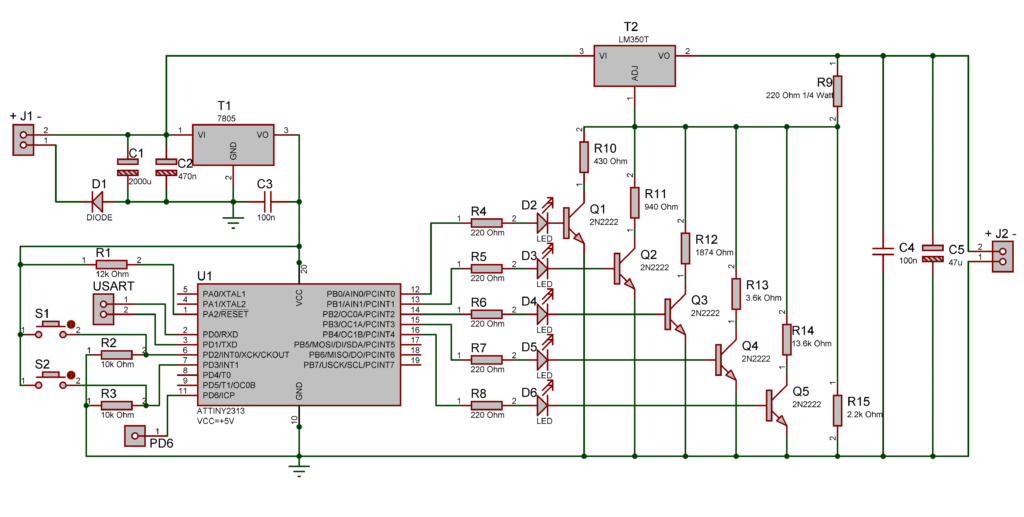
The hart of this circuit is a LM350 adjustable positive voltage regulator (T2). The voltage regulator is capable of supplying in excess of 3 amps over an output voltage range of 1.2Vdc to 33Vdc. Its ease of use, thermal overload protection, large voltage range, current limiting, and high ripple rejection make it a great choice for a variable power supply. The voltage (on the Vout pin) is regulated by the current traveling out the ADJ pin through a resistor to ground. Therefore by changing the resistance the outputted voltage will change.

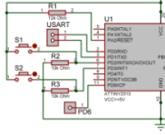
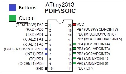
Changing the resistance is controlled by an Atmel ATtiny2313 microcontroller (U1). The microcontroller has 2 main functions collecting user input and changing the output. Collecting user input is easy; there are two buttons (S1-S2), one to go to the next voltage and the other to go to the previous voltage. The buttons are connected to the microcontroller pins PD2 and PD3. When a button is pressed the microcontroller sees a high signal (+5 volts) on the corresponding pin. The rest of the time, when a button is not pressed the microcontroller sees a low signal (0 volts) on the corresponding pin because the pin in connected to ground trough a resistor (R2-R3), called a pull down resistor.

image_1

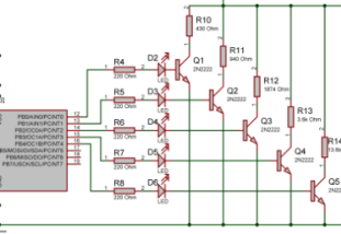
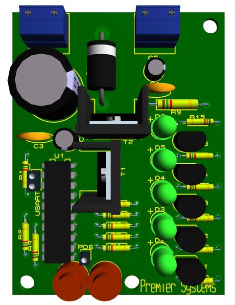
When the microcontroller sees an input pin change from low to high, it sends a high signal (+5 volts) to an output pin. There are five output pins PB0 PB1 PB2 PB3 PB4, each going through a small current limiting resistor (R4-R8) to a led (D2-D6), so you can see what the current selected voltage is, then to the base pin of a small 2n2222 transistor (Q1-Q5).

image_2

Each transistor has a resistor connected to its collector pin and its emitter pin connected to ground. When the transistor receives voltage on its base pin, power will flow from the collector to the emitter. This basically turns a resistor on or off which changes the current on the ADJ pin of the LM350 (T2).

The LM7805 (T1) is just a basic fixed 5 volt dc regulator to provide power to the microcontroller.
Diode D1 protects the circuit from a positive voltage being attached to ground.
Capacitors C1 C2 C3 C4 and C5 are used to keep steady power and decouple parts of the circuits.

The LEDs don’t need to be mounted to the PCB. They can be mounted in a panel to easily display the selected voltage, or excluded completely and replaced with a jumper wire. They are currently set at the following values:

D2 -> 3.3v, D3 -> 5v, D4 -> 7v, D5 -> 9v, D6 -> 12v

Changing the value of R9-R15 will change the preset voltages to any voltage you want.

image_3

Where Ra is the component R9 and Rb is the component R10-R14 in parallel with R15. Remember that R10-R14 is in parallel with R15 and their value needs to be calculated as such.

image_4

Schematic

mcu_power_supply_schematic

Diagramms

Diagrams

ATtiny2313_Pinout

Parts List

Quantity Reference Description
1 R1 12k Ohm 1/8 Watt Resistor
2 R2, R3 10k Ohm 1/8 Watt Resistor
5 R4-R8 220 Ohm 1/8 Watt Resistor
1 R9 220 Ohm 1/4 Watt Resistor
1 R10 430 Ohm 1/8 Watt Resistor
1 R11 940 Ohm 1/8 Watt Resistor
1 R12 1874 Ohm 1/8 Watt Resistor
1 R13 3.6k Ohm 1/8 Watt Resistor
1 R14 13.6k Ohm 1/8 Watt Resistor
1 R15 2.2k Ohm 1/8 Watt Resistor
1 C1 2000uF  50v Capacitor
1 C2 470nF  50v Capacitor
2 C3, C4 100nF  Capacitor
1 C5 47uF  Capacitor
1 U1 Atmel ATTINY2313 Microcontroller
5 Q1-Q5 2N2222 NPN Transistor
1 D1 1N5402 3 Amp Diode
5 D2-D6 5mm generic LED
1 T1 7805 voltage regulator 5volt
1 T2 LM350T
2 S1, S2 Generic Momentary Switch or Button
2 J1*, J2* Tyco 282841-2

*Not necessary

MCU Programming

The C# code for the microcontroller is in the file:  MCU_Power_Supply
It can be easily modified to control 36 different voltages with this same circuit.

Set the SUT_CKSEL fuse to: “Int. RC Osc. 4 MHz; Start-up time: 14 CK + 65 ms”
Make sure the CKDIV8 fuse is not set.

The PCB also has connections for Rx Tx and PD6 so that an LCD display, computer control, and extra inputs and outputs can easily be added.

MCU_Power_Supply_3D_Overhead_th

Links

LM350 http://www.fairchildsemi.com/ds/LM%2FLM350.pdf

2N2222 http://www.onsemi.com/pub_link/Collateral/P2N2222A-D.PDF

ATtiny2313 http://www.atmel.com/dyn/resources/prod_documents/2543S.pdf

Mini variable power supply

Schematic

Description

T1 steps down AC voltage from 115VAC (or 220VAC) to about 8VAC and is then rectified via bridge rectifier BR1 to about 11.52Vdc. C1 filters off the AC ripple. If you find the circuit output too noisy add another electrolytic capacitor over the output terminals. Value can be between 10 and 100uF/25V. The output voltage is variable with the 10K-potentiometer while keeping the current constant.

Description

T1 = 115/8 VAC transformer. Center Tap not needed.
Q1 = 2N1613, NTE128, or substitute. (TO-39 case) On coolrib!
BR1 = 40V, 4A. (Check max current of your mini-drill and add 2A)
R1 = 470 ohm, 5%
R2 = 1K, 5%
P1 = Potentiometer, 10K
C1 = 1000uF, 25V, electrolytic
C2 = 0.1uF (100nF), ceramic

Charger for mobile phones

Schematic

Description

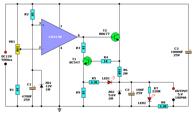
Most mobile chargers do not have current/voltage reguLation or short-circuit protection. These chargers provide raw 6-12V DC for charging the battery pack. Most of the mobile phone battery packs have a rating of 3.6V, 650 mAh. For increasing the life of the battery, slow charging at low current is advisable. Six to ten hours of charging at 150-200mA current is a suitable option. This will prevent heating up of the battery and extend its life. The circuit described here provides around 180mA current at 5.6V and protects the mobile phone from unexpected voltage fluctuations that develop on the mains line. So the charger can be left ‘on’ over night to replenish the battery charge. The circuit protects the mobile phone as well as the charger by immediately disconnecting the output when it senses a voltage surge or a short circuit in the battery pack or connector. It can be called a ‘middle man’ between the existing charger and the mobile phone. It has features like voltage and current regulation, over-current protection, and high- and low-voltage cut-off. An added speciality of the circuit is that it incorporates a short delay of ten seconds to switch on when mains resumes following a power failure. This protects the mobile phone from instant voltage spikes. The circuit is designed for use in conjunction with a 12V, 500mA adaptor (battery eliminator). Op-amp IC CA3130 is used as a voltage comparator. It is a BiMOS operational amplifier with MOSFET input and CMOS output. Inbuilt gate-protected p-channel MOSFETs are used in the input to provide very high input impedance. The output voltage can swing to either positive or negative (here, ground) side. The inverting input (pin 2) of IC1 is provided with a variable voltage obtained through the wiper of potmeter VR1. The non-inverting input (pin 3) of IC1 is connected to 12V stabilised DC voltage developed across zener ZD1. This makes the output of IC1 high.

After a power resumption, capacitor C1 provides delay of a few seconds to charge to a potential higher than of inverting pin 2 of CA3130, thus the output of IC1 goes high only after the delay. In the case of a heavy power line surge, zener diode ZD1 (12V, 1W) will breakdown and short pin 3 of IC1 to ground and the output of IC1 drops to ground level. The output of IC1 is fed to the base of npn Darlingtontransistor BD677 (T2) for charging the battery. Transistor T2 conducts only when the output of IC1 is high. During conduction the emitter voltage of T2 is around 10V, whichpasses through R6 to restrict the charging current to around 180 mA. Zener diode ZD2 regulates the charging voltage to around 5.6V. When a short-circuit occurs at the battery terminal, resistor R8 senses the over-current, allowing transistor T1 to conduct and light up LED1. Glowing of LED2 indicates the charging mode, while LED1 indicates shortcircuit or over-current status. The value of resistor R8 is important to get the desired current level to operate the cut-off. With the given value of R8 (3.3 ohms), it is 350 mA. Charging current can also be changed by increasing or decreasing the value of R7 using the ‘I=V/R’ rule. Construct the circuit on a common PCB and house in a small plastic case. Connect the circuit between the output lines of the charger and the input pins of the mobile phone with correct polarity.

Li-Ion Charger

Schematic

Description

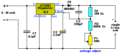
The LP2951 regulator is manufactured by National Semiconductors. The choice of values is from an application note “Battery Charging”, written by Chester Simpson.

Diode D1 can be any diode from the 1N00x series, whichever is conveniently available. It functions as a blocking diode, to prevent a back flow of current from the battery into the LP2951 when the input voltage is disconnected.

Charging current is about 100+mA, which is the internally-limited maximum current of the LP2951. For those wondering, this is compatible with just about any single-cell li-ion battery since li-ion can generally accept a charging current of up to about 1c (i.e. charging current in mA equivalent to their capacity in mAh, so a 1100mAh li-ion cell can be charged at up to 1100mA and so on). A lower charging current just brings about a correspondingly longer charge time. IMHO 100mA is quite low, low enough that the circuit can be used for an overnight charger for many typical single-cell li-ion batteries.
The resistors are deliberately kept at large orders of magnitude (tens/hundred Kohm and Mohm range) to keep the off-state current as low as possible, at about 2΅A. Resistor tolerances should be kept at 1% for output voltage accuracy. The 50k pot allows for an output voltage range between 4.08V to 4.26V – thus allowing calibration as well as a choice between a charging voltage of 4.1V or 4.2V depending on the cell to be charged. The capacitors are for stability, especially C2 which prevents the output from ringing/oscillating.

Parts List

IC1 = LP2951, voltage regulator
D1 = 1N4002, General purpose diode
R1 = 2M, 1%, metal-film
R2 = 806K, 1%, metal-film
P1 = 50K, potentiometer
C1 = 0.1uF, polyester
C2 = 2.2uF/16V, electrolytic
C3 = 330pF, ceramic

Lead Acid Battery Charger #2

Schematic

Description

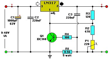
The above pictured schematic diagram is just a standard constant current model with a added current limiter, consisting of Q1, R1, and R4. The moment too much current is flowing biases Q1 and drops the output voltage.

The output voltage is: 1.2 x (P1+R2+R3)/R3 volt. Current limiting kicks in when the current is about 0.6/R1 amp.
For a 6-volt battery which requires fast-charging, the charge voltage is 3 x 2.45 = 7.35 V. (3 cells at 2.45v per cell). So the total value for R2 + P1 is then about 585 ohm. For a 12 V battery the value for R2 + P1 is then about 1290 ohm.

For this power supply to work efficiently, the input voltage has to be a minimum of 3V higher than the output voltage.

P1 is a standard trimmer potentiometer of sufficient watt for your application.

The LM317 must be cooled on a sufficient (large) coolrib.

Q1 (BC140) can be replaced with a NTE128 or the older ECG128 (same company).

Except as a charger, this circuit can also be used as a regular power supply.

Parts List

Parts List:
R1 = 0.56 Ohm, 5W, WW
R2 = 470 Ohm C2 = 220nF
R3 = 120 Ohm
R4 = 100 Ohm
C1 = 1000uF/63V
Q1 = BC140
Q2 = LM317, Adj. Volt Reg.
C3 = 220nF (On large coolrib!)
P1 = 220 Ohm

Lead Acid Battery Charger #1

Schematic

Description

Except for use as a normal Battery Charger, this circuit is perfect to ‘constant-charge’ a 12-Volt Lead-Acid Battery, like the one in your flight box, and keep it in optimum charged condition. This circuit is not recommended for GEL-TYPE batteries since it draws to much current.

The above circuit is a precision voltage source, and contains a temperature sensor with a negative temperature coλficient. Meaning, whenever the surrounding or battery temperature increases the voltage will automatically decrease. Temperature coλficient for this circuit is -8mV per °Celcius. A normal transistor (Q1) is used as a temperature sensor.

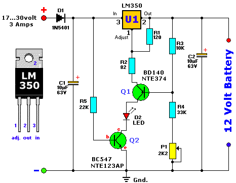
This Battery Charger is centered around the LM350 integrated, 3-amp, adjustable stabilizer IC. Output voltage can be adjusted with P1 between 13.5 and 14.5 volt. T2 was added to prevent battery discharge via R1 if no power present. P1 can adjust the output voltage between 13.5 and 14.5 volts. R4’s value can be adjusted to accommodate a bit larger or smaller window. D1 is a large power-diode, 100V PRV @ 3 amp. Bigger is best but I don’t recommend going smaller. The LM350’s ‘adjust’ pin will try to keep the voltage drop between its pin and the output pin at a constant value of 1.25V. So there is a constant current flow through R1.

Q1 act here as a temperature sensor with the help of components P1/R3/R4 who more or less control the base of Q1. Since the emitter/base connection of Q1, just like any other semiconductor, contains a temperature coλficient of -2mV/°C, the output voltage will also show a negative temperature coλficient. That one is only a factor of 4 larger, because of the variation of the emitter/basis of Q1 multiplied by the division factor of P1/R3/R4. Which results in approximately -8mV/°C. To prevent that sensor Q1 is warmed up by its own current draw, I recommend adding a cooling rib of sorts. (If you wish to compensate for the battery-temperature itself, then Q1 should be mounted as close on the battery as possible) The red led (D2) indicates the presence of input power.Depending on what type of transistor you use for Q1, the pads on the circuit board may not fit exactly (in case of the BD140).

Simple 78xx Current Booster

Schematic

Description

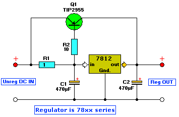
Voltage regulators such as the LM78xx, and LM317 series (and others) sometimes need to provide a little bit more current then they actually can handle. If that is the case, this little circuit can help out. A power transistor such as the 2N3772 or similar can be used (See the project on the 3-part variable power supply).

The power transistor is used to boost the extra needed current above the maximum allowable current provided via the regulator. Current up to 1500mA(1.5amp) will flow through the regulator, anything above that makes the regulator conduct and adding the extra needed current to the output load.

It is no problem stacking power transistors for even more current. (see diagram). Both the regulator and power transistor must be mounted on an adequate heatsink.

LM7805 Datasheet

TOP PCB Companies