MAX2606 – Hands-Free Car Kit for Cell Phones

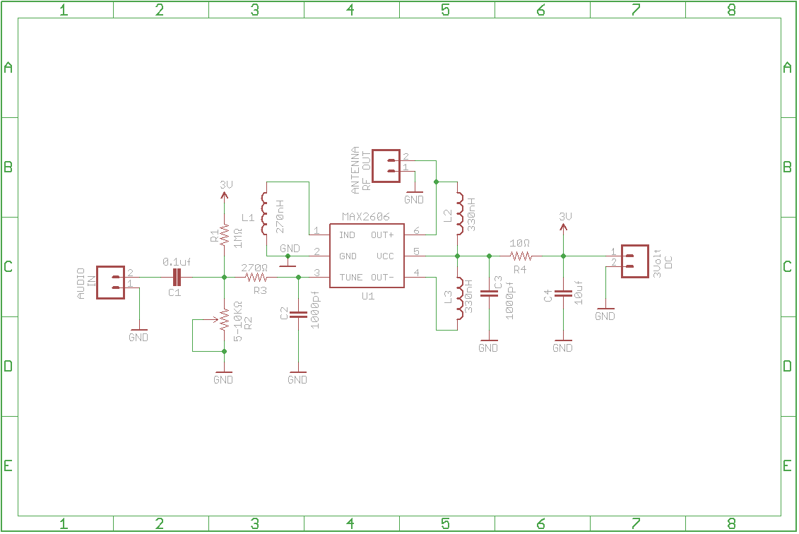
MAX2606_Schematic

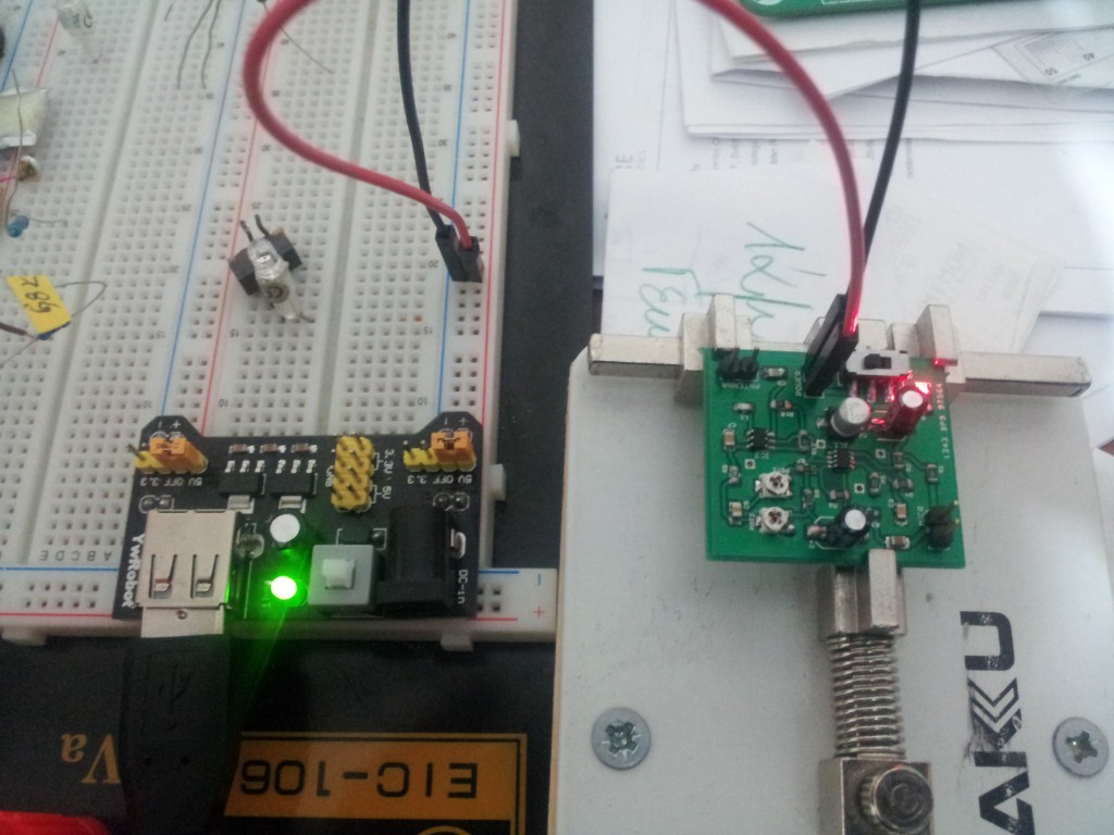
This project is car hands free that retransmits the audio signal from a cell phone to the FM broadcast band. By placing the cell phone’s speaker near the microphone, the user can use the phone as a hands-free device while driving.

Specifications

  • Power supply: +2.7V to +5.5V stab – 2.1mA
  • RF power: -10dBm
  • Impedance: 50-75 ohm
  • Frequency range: 70 – 150 MHz
  • Integrated Varactor for Tuning

Description

This project is based on MAXIM’s App Note 5123

This is a FM transmitter circuit with a direct audio input that eliminates background noise from the microphone. The electret microphone is biased with R1. The AC-coupled microphone audio signal modulates the VCO frequency by changing VTUNE. The output frequency of the VCO will follow the volume or amplitude from the microphone.
An audio signal with approximately 20mVRMS is adequate for functionality.

Do not over-modulate the VCO, or the resulting audio from the FM receiver will be distorted.

Over-modulating the VCO also weakens the carrier signal by emitting power onto the unused spectrum by the receiver.

In Figure, the microphone and R1 are replaced with a direct connection to the audio output port of a cell phone.

The cell phone’s volume needs to be adjusted accordingly for optimal performance.
A direct connection to the cell phone will eliminate background noise from the microphone.

Thanks Maxim for samples – by spilkos.

Photos

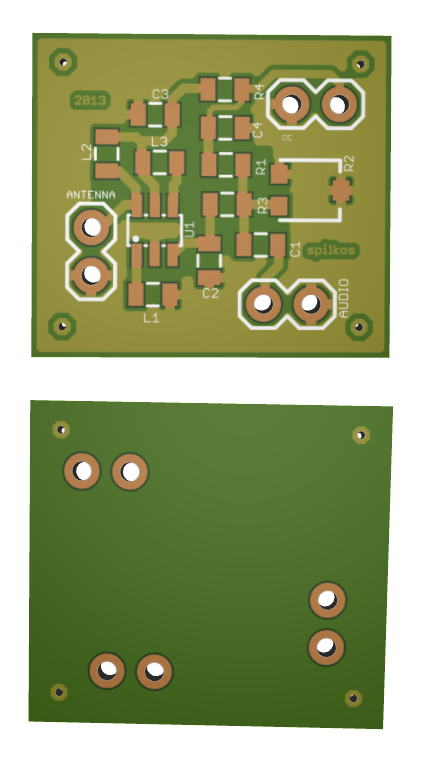
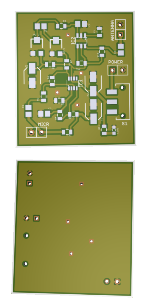
3D_PCB

3D PCB rendering

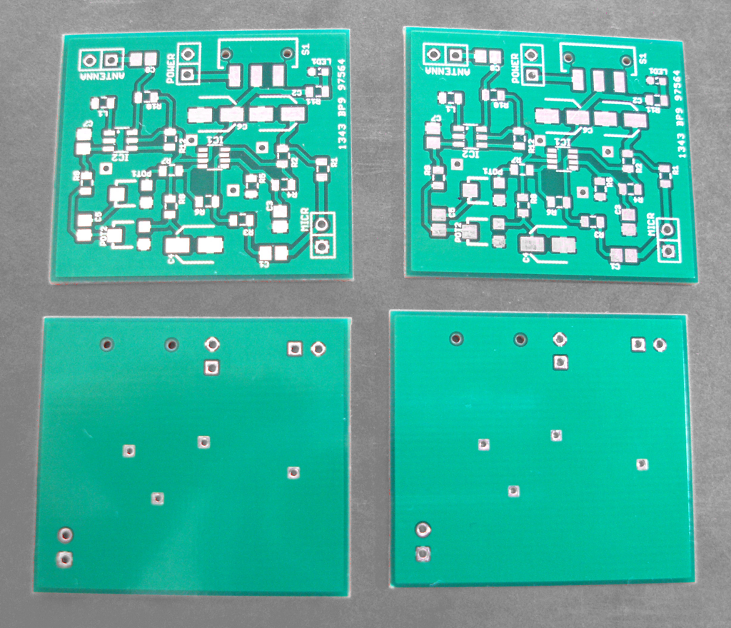
photo_1

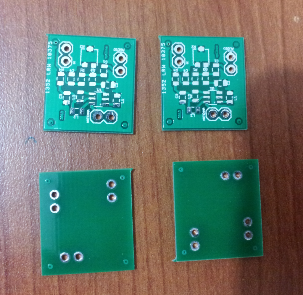
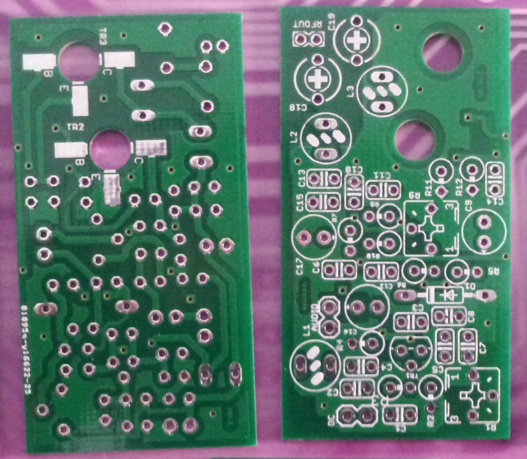
manufactured PCBs

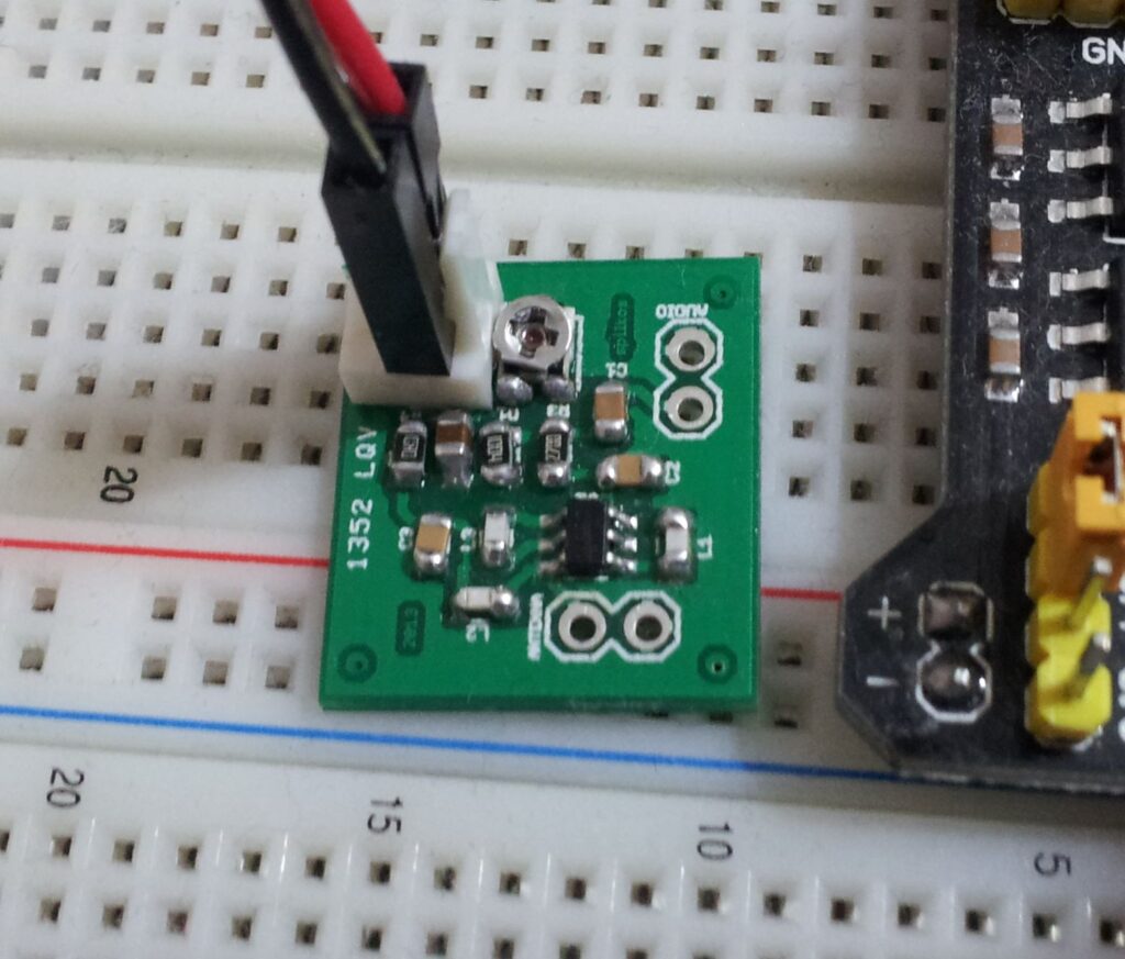
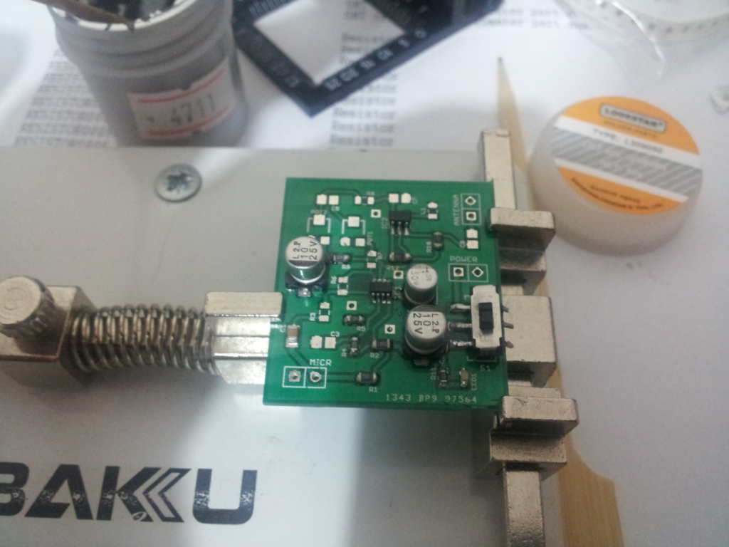
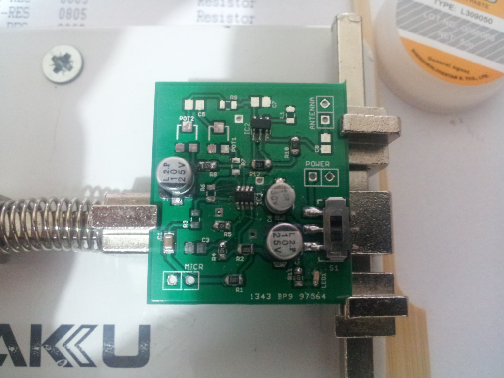
photo_2

FM VCO Transmitter

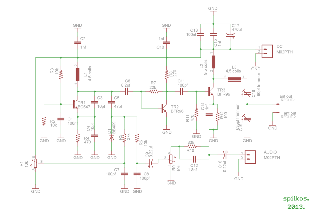
schematic

This is a VCO FM Transmitter with range 500m – 4km depending on antenna used.

Specifications

  • Power supply: 12-14 V stab., 100 mA
  • RF power: 400 mW
  • Impedance: 50-75 ohm
  • Frequency range: 87,5-108 MHz
  • Modulation: wideband FM

Description

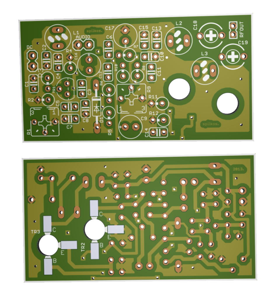
This circuit originally published on www.pira.cz but a new PCB design is introduced here.

Connect the 6 V / 0,1 A bulb to the output and use R1 to tune the right frequency. Maybe you might stretch coils of the L1. Then use C14 and C15 to adjust the highest power (the highest light of the bulb). Then you can connect antenna and audio signal.

Adjust R2 until the audio sounds as loud as the other stations. With good antenna (dipole placed outdoor and high) the transmitter has very good coverage range about 500 meters, the maximal coverage range is up to 4 km.

Photos

3D_PCB

pcb_photo

photo_1

photo_2

FM Transmitter using MAX4467 & MAX2606

FM_transmitter_Schematic


his is a small circuit with two maxim’s ic, MAX4467 as microphone amplifier and MAX406 as VCO FM transmitter. It’s suitable for short range FM transmittion aka wireless FM microphone.

Description

This article originally published on in issue 323, July 2003 of Elektor magazine but a new PCB design is introduced here.

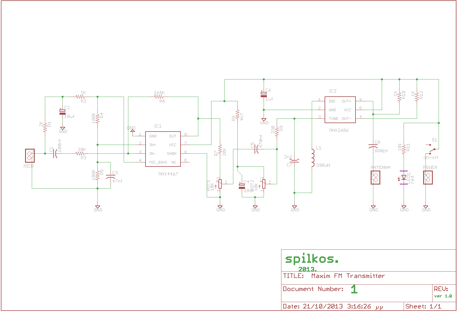
Here is a very simple, inexpensive and interesting project which provides lot of fun to a home experimenter or hobbyist. This simple transmitter can transmit speech over a short range. It can be used as a simple cordless microphone. The circuit uses two integrated circuits from Maxim. IC1 a MAX4467, is an amplifier raising the microphone signal to a level suitable for frequency modulation (FM). IC2 is a voltage-controlled oscillator (VCO) with integrated varactor (a.k.a. varicap diode). Its nominal frequency of oscillation is set by inductor L1. The inductor value 390 nH provides an oscillation frequency of about 100 MHz. For best performance, L1 should be a high-Q component. L1 may consist of 4 turns of silver-plated wire wound around a 10-mm drill bit, and stretched to a length of about 1.5 cm.

The wire diameter can be anything between 26 SWG (0.5 mm) and 20 SWG (1 mm). No core is used. The MAX4467 is a micro-power opamp for low voltage operation and providing 200-kHz gain bandwidth at a supply current of just 24 ΅A. When used with an electret microphone, some form of DC bias for the microphone capsule is necessary. The MAX4467 has the ability to turn off the bias to the microphone when the device is in shutdown mode. This can save several hundred micro-amps of supply current, which can be significant in low power applications particularly for battery powered applications like cordless microphones. The MIC-Bias pin provides a switched version of Vcc to the bias components.

Resistor R1 resistor limits the current to the microphone element. The output impedance of the MAX4467 is low and well suited to driving cables over distances up to 50 m. The MAX2606 intermediate-frequency (IF) voltage-controlled oscillators (VCO) has been designed specifically for portable wireless communication systems. The IC comes in a tiny 6-pin SOT23 package. The low-noise VCO features an on-chip varactor and feedback capacitors that eliminate the need for external tuning elements. Only an external inductor (here, L1) is required to set the oscillation frequency and produce a properly operating VCO. To minimize the effects of parasitic elements, which degrade circuit performance, place L1 and C5 close to their respective pins.

Specifically, place C5 directly across pins 2 (GND) and 3 (TUNE). Potentiometer P2 then lets you select a free channel by tuning over the FM band of 88 MHz to 108 MHz. Output power is about –21dBm (approx. 10΅W) into 50 Ω. P1 serves as a volume control by modulating the RF frequency. Signals above 60mV introduce distortion, so the pot attenuates from that level. To decrease stray capacitance, minimize trace lengths by placing external components close to IC1’s pins. Using a wire antenna of about 75 cm the transmitter should have a range of about 35 m. Try to keep all leads as short as possible to prevent stray capacitance. The transmitter operates on a single supply voltage in the range 4.5 V to 5.5 V from any standard battery source. The transmitter must be housed in a metal case, with shielding installed between the two stages (AF and RF). Try to keep all leads as short as possible to prevent stray capacitance.

PCB

3D_PCB_full

pcb_photos

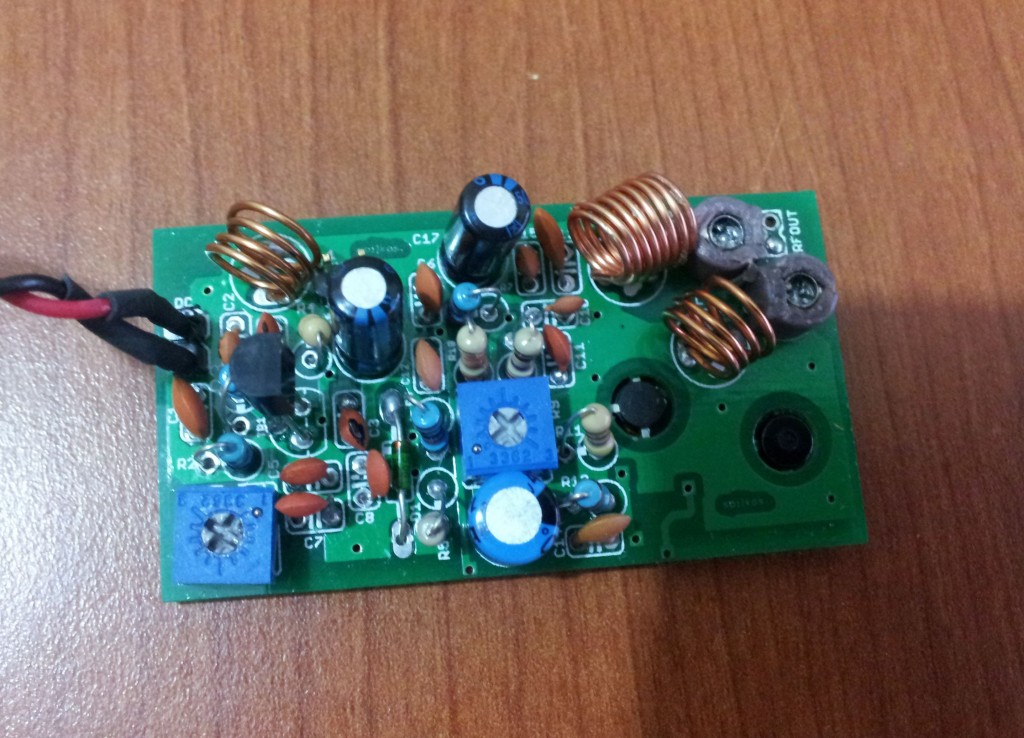
photo_2

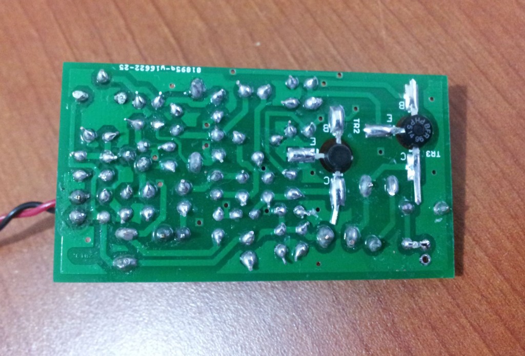
photo_3

photo_4

4 Watt FM Transmitter

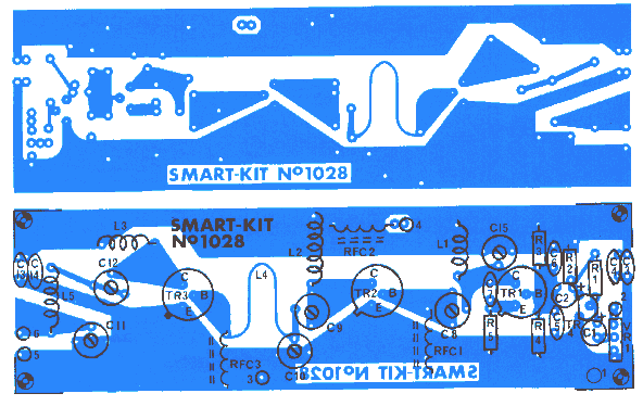
1028

Copyright of this circuit belongs to smart kit electronics. In this page we will use this circuit to discuss for improvements and we will introduce some changes based on original schematic.

General Description

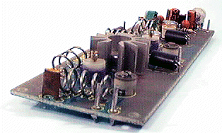
This is a small but quite powerful FM transmitter having three RF stages incorporating an audio preamplifier for better modulation. t has an output power of 4 Watts and works off 12-18 VDC which makes it easily portable. It is the ideal project for the beginner who wishes to get started in the fascinating world of FM broadcasting and wants a good basic circuit to experiment with.

Technical Specifications – Characteristics

  • Modulation type: FM
  • Frequency range: 88-108 MHz
  • Working voltage: 12-18 VDC
  • Maximum current: 450 mA
  • Output power: 4 W

How it Works

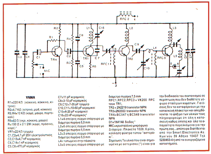
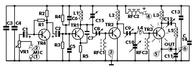
As it has already been mentioned the transmitted signal is Frequency Modulated (FM) which means that the carrier’s amplitude stays constant and its frequency varies according to the amplitude variations of the audio signal. When the input signal’s amplitude increases (i.e. during the positive half cycles) the frequency of the carrier increases too, on the other hand when the input signal decreases in amplitude (negative half-cycle or no signal) the carrier frequency decreases accordingly. In figure 1 you can see a graphic representation of Frequency Modulation as it would appear on an oscilloscope screen, together with the modulating AF signal. The output frequency the transmitter is adjustable from 88 to 108 MHz which is the FM band that is used for radio broadcasting. The circuit as we have already mentioned consists of four stages. Three RF stages and one audio preamplifier for the modulation. The first RF stage is an oscillator and is built around TR1. The frequency of the oscillator is controlled by the LC network L1-C15. C7 is there to ensure that the circuit continues oscillating and C8 adjusts the coupling between the oscillator and the next RF stage which is an amplifier. This is built around TR2 which operates in class C and is tuned by means of L2 and C9. The last RF stage is also an amplifier built around TR3 which operates in class C the input of which is tuned by means of C10 and L4. From the output of this last stage which is tuned by means of L3-C12 is taken the output signal which through the tuned circuit L5-C11 goes to the aerial.

The circuit of the preamplifier is very simple and is built around TR4. The input sensitivity of the stage is adjustable in order to make it possible to use the transmitter with different input signals and depends upon the setting of VR1. As it is the transmitter can be modulated directly with a piezoelectric microphone, a small cassette recorder etc. It is of course possible to use an audio mixer in the input for more professional results.

Construction

First of all let us consider a few basics in building electronic circuits on a printed circuit board. The board is made of a thin insulating material clad with a thin layer of conductive copper that is shaped in such a way as to form the necessary conductors between the various components of the circuit. The use of a properly designed printed circuit board is very desirable as it speeds construction up considerably and reduces the possibility of making errors. Smart Kit boards also come pre-drilled and with the outline of the components and their identification printed on the component side to make construction easier. To protect the board during storage from oxidation and assure it gets to you in perfect condition the copper is tinned during manufacturing and covered with a special varnish that protects it from getting oxidised and also makes soldering easier. Soldering the components to the board is the only way to build your circuit and from the way you do it depends greatly your success or failure. This work is not very difficult and if you stick to a few rules you should have no problems. The soldering iron that you use must be light and its power should not exceed the 25 Watts. The tip should be fine and must be kept clean at all times. For this purpose come very handy specially made sponges that are kept wet and from time to time you can wipe the hot tip on them to remove all the residues that tend to accumulate on it. DO NOT file or sandpaper a dirty or worn out tip. If the tip cannot be cleaned, replace it. There are many different types of solder in the market and you should choose a good quality one that contains the necessary flux in its core, to assure a perfect joint every time. DO NOT use soldering flux apart from that which is already included in your solder. Too much flux can cause many problems and is one of the main causes of circuit malfunction. If nevertheless, you have to use extra flux, as it is the case when you have to tin copper wires, clean it very thoroughly after you finish your work.

In order to solder a component correctly you should do the following:

  • Clean the component leads with a small piece of emery paper.
  • Bend them at the correct distance from the component’s body and insert the component in its place on the board.
  • You may find sometimes a component with heavier gauge leads than usual, that is too thick to enter in the holes of the p.c. board. In this case, use a mini drill to enlarge the holes slightly.
  • Do not make the holes too large as this is going to make soldering difficult afterward.
  • Take the hot iron and place its tip on the component lead while holding the end of the solder wire at the point where the lead emerges from the board. The iron tip must touch the lead slightly above the p.c. board. – When the solder starts to melt and flow wait till it covers evenly the area around the hole and the flux boils and gets out from underneath the solder. The whole operation should not take more than 5 seconds. Remove the iron and allow the solder to cool naturally without blowing on it or moving the component. If everything was done properly the surface of the joint must have a bright metallic finish and its edges should be smoothly ended on the component lead and the board track. If the solder looks dull, cracked, or has the shape of a blob then you have made a dry joint and you should remove the solder (with a pump, or a solder wick) and redo it.
  • Take care not to overheat the tracks as it is very easy to lift them from the board and break them.
  • When you are soldering a sensitive component it is good practice to hold the lead from the component side of the board with a pair of long-nose pliers to divert any heat that could possibly damage the component.
  • Make sure that you do not use more solder than it is necessary as you are running the risk of short-circuiting adjacent tracks on the board, especially if they are very close together.
  • When you finish your work cut off the excess of the component leads and
    clean the board thoroughly with a suitable solvent to remove all flux residues that may still remain on it.

This is an RF project and this calls for even more care during soldering as sloppiness during construction can mean low or no output at all, low stability and other problems. Make sure that you follow the general rules about electronic circuit construction outlined above and double-check everything before going to the next step. All the components are clearly marked on the component side of the P.C. board and you should have no difficulty in locating and placing them. Solder first of all the pins, and continue with the coils taking care not to deform them, the RFC’s, the resistors, the capacitors and finally the electrolytic and the trimmers. Make sure that the electrolytic are correctly placed with respect to their polarity and that the trimmers are not overheated during soldering. At this point stop for a good inspection of the work done so far and if you see that everything is OK go on and solder the transistors in their places taking grate care not to overheat them as they are the most sensitive of all the components used in the project. The audio frequency input is at points 1 (ground) and 2 (signal), the power supply is connected at points 3 (-) and 4 (+) and the antenna is connected at points 5 (ground) and 6 (signal). As we have already mentioned the signal you use for the modulation of the transmitter could be the output of a preamplifier or mixer or in case you only want to modulate it with voice you can use the piezoelectric microphone supplied with the Kit. (The quality of this microphone is not very good but it is quite adequate if you are interested in speech only.) As an antenna you can use an open dipole or a Ground Plane. Before you start using the transmitter or every time you change its working frequency you must follow the procedure described below which is called alignment.
fm2

Parts List

R1 = 220K
R2 = 4,7K
R3 = R4 = 10K
R5 = 82 Ohm
R = 150Ohm 1/2W x2 *
VR1 = 22K trimmer

C1 = C2 = 4,7uF 25V electrolytic
C3 = C13 = 4,7nF ceramic
C4 = C14 = 1nF ceramic
C5 = C6 = 470pF ceramic
C7 = 11pF ceramic
C8 = 3-10pF trimmer
C9 = C12 = 7-35pF trimmer
C10 = C11 = 10-60pF trimmer
C15 = 4-20pF trimmer
C16 = 22nF ceramic *

L1 = 4 turns of silver coated wire at 5,5mm diameter
L2 = 6 turns of silver coated wire at 5,5mm diameter
L3 = 3 turns of silver coated wire at 5,5mm diameter
L4 = printed on PCB
L5 = 5 turns of silver coated wire at 7,5mm diameter

RFC1=RFC2=RFC3= VK200 RFC tsok

TR1 = TR2 = 2N2219 NPN
TR3 = 2N3553 NPN
TR4 = BC547/BC548 NPN
D1 = 1N4148 diode *
MIC = crystalic microphone

Note: Parts marked with * are used for the tune-up of the transmitter in case you have not a stationary wave bridge.

Adjustments

If you expect your transmitter to be able to deliver its maximum output at any time you must align all the RF stages in order to ensure that you get the best energy transfer between them. There are two ways to do this and it depends if you have a SWR meter or not which method you are going to follow. If you have a SWR meter turn the transmitter on, having connected the SWR meter in its output in series with the antenna, and turn C15 in order to tune the oscillator to the frequency you have chosen for your broad casts. Then start adjusting the trimmers C8,9,10,12 and 11 in this order till you get the maximum output power in the SWR meter. For those who don’t have a SWR meter there is another method which gives quite satisfactory results. You only have to build the little circuit in Fig. 2 which is connected in the out put of the transmitter and in its output (across C16) you connect your multi-tester having selected a suitable VOLTS scale. You tune C15 in the desired frequency and then adjust the other trimmers in the same order as it is described above for the maximum output in the multitester. The disadvantage of this method is that you do not align the transmitter with a real antenna connected in its output and it may be necessary to make slight adjustments to C11 and C12 for a perfect antenna match.
Do not forget to align your transmitter every time you change your aerial or your working frequency.
WARNING: In every transmitter there are present apart from the main output frequency various harmonics that usually have a very short range. In order to make sure you haven’t tuned on one of them do the tuning as far as possible from your receiver, or use a Spectrum Analyser to see your output spectrum and make sure that you tune your transmitter on the right frequency.

Warning

Smart kits are sold as stand alone training kits.
If they are used as part of a larger assembly and any damage is caused, our company bears no responsibility.

While using electrical parts, handle power supply and equipment with great care, following safety standards as described by international specs and regulations.

CAUTION
All the RF kits are sold for experimental and laboratory use only. Their possession and use are limited by laws which vary from state to state. Please get information about what you can or can not do in your area and stay within the legal limits. Make sure you do not become a nuisance to others with your experiments. Smart Kit has no responsibility whatsoever for any misuse of its products.

If it does not work

  • Check your work for possible dry joints, bridges across adjacent tracks or soldering flux residues that usually cause problems.
  • Check again all the external connections to and from the circuit to see if there is a mistake there.
  • See that there are no components missing or inserted in the wrong places.
  • Make sure that all the polarised components have been soldered the right way round.
  • Make sure that the supply has the correct voltage and is connected the right way round to your circuit.
  • Check your project for faulty or damaged components.

Electronic Diagram
1028d

fm1

Also check this site for additional information

Improvements on original design

Thomas [thomasciciyan @ yahoo.com] made some improvement on original design:

  • The ability for capacitor microphone
  • Preamplifier for the mic
  • External audio input jack, for example: to transmit sounds from a computer audio card
  • A selector switch to select microphone or input jack
  • PCB redesign

Parts added

C17 (1uf)
C18 (4uf7)
C19 (4uf7)
C20 (100NF)

H1 (13*13*10MM)
JACK1 (STEREO)

LED2 (RED)
MIC (CAPACITIC)

R6 (1M8)
R7 (1K5)
R8 (560K)

R9 (820R)
R10 (4K7)
R11 (4K7)

R12 (1K)
R13 (1K)
R14 (2K2)

R15 (680R)
TR5 (BC547\BC548)

VR1 (50K)

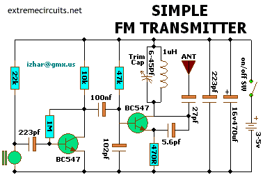
Simple FM Transmitter

SIMPLE FM TRANSMITTER


Description

This FM transmitter (FM Tx) is about the simplest and most basic FM Tx it is possible to build and have a useful transmitting range. It is surprisingly powerful despite its small component count and 3V operating voltage. It will easily penetrate over three floors of an apartment building and go over 300 meters in the open air. The circuit we use is based on a proven Australian design. It may be tuned anywhere in the FM band. Or it may be tuned outside the commercial M band for greater privacy. (Of course this means you must modify your FM radio to be able to receive the transmission or have a broad-band FM receiver.) The output power of this FM Tx is below the legal limits of many countries (eg, USA and Australia). However, some countries may ban ALL wireless transmissions without a license. It is the responsibility of the builder to check the legal requirements for the operation of this circuit and to obey them.
The circuit is basically a radio frequency (RF) oscillator that operates around 100 MHz. Audio picked up and amplified by the electret microphone is fed into the audio amplifier stage built around the first transistor. Output from the collector is fed into the base of the second transistor where it modulates the resonant frequency of the tank circuit (the 5 turn coil and the trimcap) by varying the junction capacitance of the transistor. Junction capacitance is a function of the potential difference applied to the base of the transistor. The tank circuit is connected in a Colpitts oscillator circuit.

Calibration

Place the transmitter about 10 feet from a FM radio. Set the radio to somewhere about 89 – 90 MHz. Walk back to the Fm Tx and turn it on. Spread the winding of the coil apart by approximately 1mm from each other. No coil winding  should be touching another winding. Use a small screw driver to tune the trim cap. Remove the screwdriver from the trim screw after every adjustment so the LC circuit is not affected by stray capacitance. Or use a plastic screwdriver. If you have difficulty finding the transmitting frequency then have a second person tune up and down the FM dial after every adjustment. One full turn of the trim cap will cover its full range of capacitance from 6pF to 45pF. The normal FM band tunes in over about one tenth of the full range of the tuning cap. So it is best to adjust it in steps of 5 to 10 degrees at each turn. So tuning takes a little patience but is not difficult. The reason that there must be at least 10 ft. separation between the radio and the Tx is that the Tx emits harmonics; it does not only emit on one frequency but on several different frequencies close to each other.

Note

You may experiment with using 6V or 9V with the circuit to see how this increases the range of the transmitter. The sensitivity may be increased by lowering the 22K resistor to 10K. Try it and see.

Frequency counter with PIC16F628A

FreqC_(16F628A)(3)


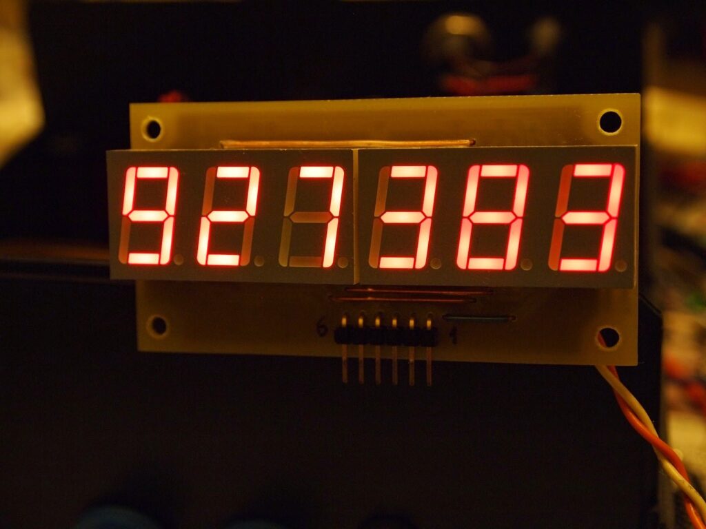
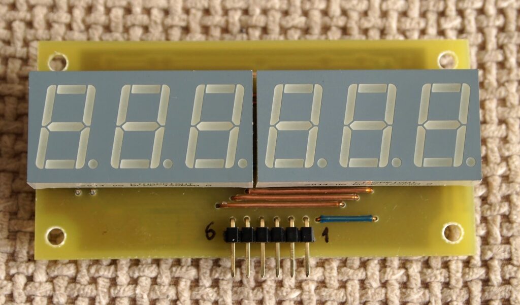
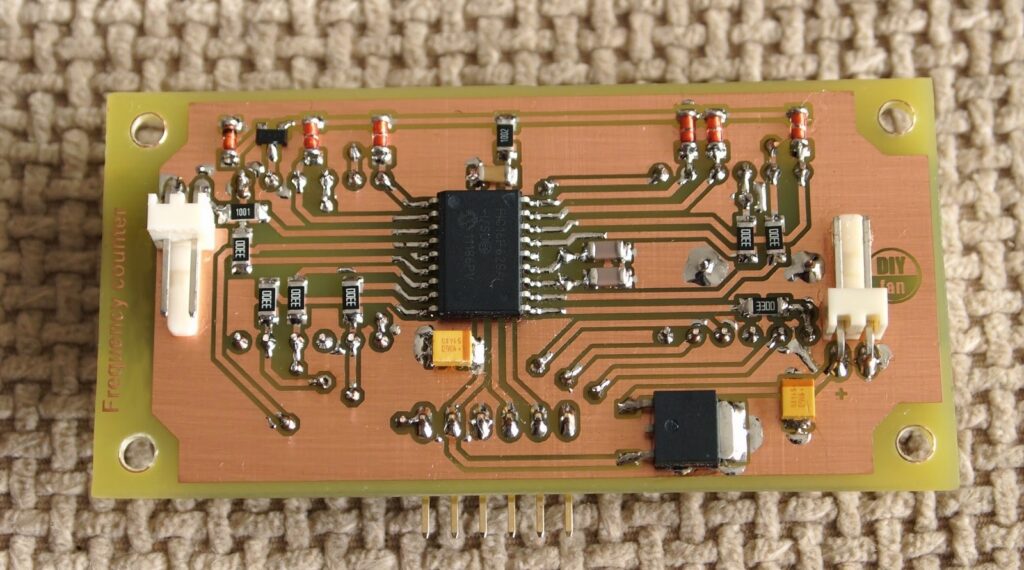
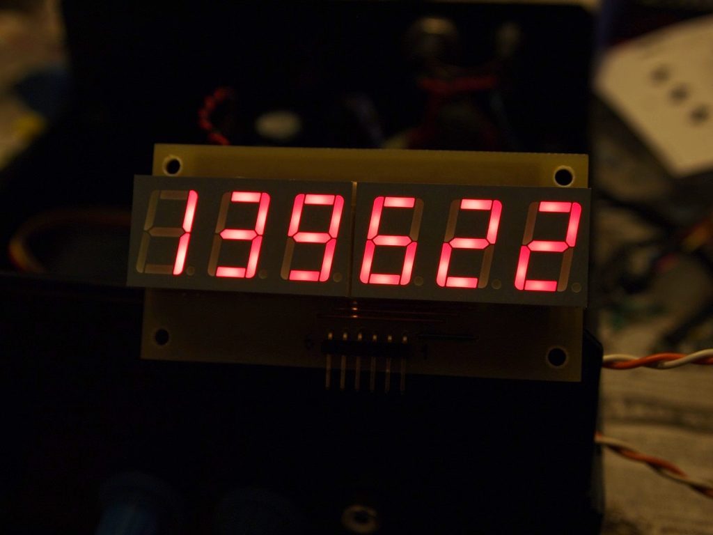
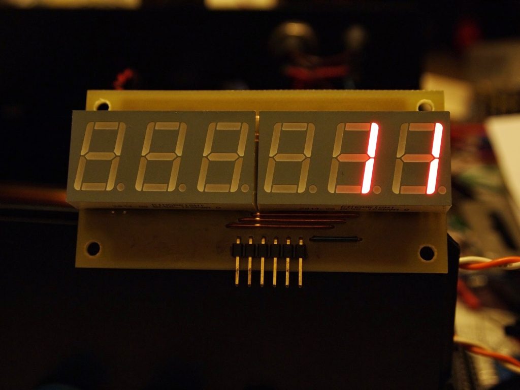
This is a frequency counter based on PIC16F628A. The original idea came from this project:LCD frequency counter. As you can see – very simple and yet elegant schematic. But I wanted to use 7-segment LED display, not LCD, so I found a second useful project: Simple 100MHz frequency counter which uses 6 digit LED display.

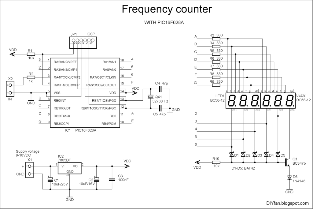
Schematic

Combining two projects into one wasn’t very easy. First of all I wanted a PIC microcontroller to do the whole job without any additional ICs. Also I wanted to use the the familiar 16F628A, but because one of the portA pins (RA5) can be used only as input I was short of outputs to do the job. Driving 6 digit 7-segment multiplexed display requires 7 + 6 = 13 outputs. The 16F628A has 16 IO pins, two of which are used for the crystal oscillator, one is for the signal input and other one can be used only for input, that leaves us with only 12 useful IO pins. The solution was to drive one of the common cathodes with a transistor, which opens when all other digits are switched off.

FreqC_(16F628A)

7-segment displays used here are 3 digit multiplexed common cathode type (BC56-12SRWA). Digits 2..5 are switched on when respective pins are set low. When all these pins are high, the transistor Q1 opens and switches on the first digit. The current for each segment is about 6-7mA.

I must mention that pins connected to common cathodes theoretically may sink up to 50mA if all segments are light up (7x7mA). This is way above max specifications of the microcontroller. But as every digit is switched on for very brief moment I think it is safe. The whole schematic consumes around 30-40mA in average and the microcontroller is not heating at all, so everything seems OK.

The microcontroller uses its internal 4MHz oscillator for the CPU clock. Timer1 uses external crystal oscillator with frequency 32768Hz for setting the 1 second time interval. Timer0 is used to count the input signal at pin RA4. And finally, Timer2 is used for cycling and refreshing the digits. As the input signal will be 5Vpp square wave there isn’t any preamp or buffer in the front.

The counter can measure up to 920-930kHz which is more than enough for my project. The reason why it can’t go higher is because driving all these digits consumes lots of CPU cycles. I suppose, the program code can be optimized or even written in assembler and then the counter can reach 999999 Hz.

The crystals for 32768Hz are sold in two sizes : 2x6mm and 3x8mm. I recommend 2x6mm because it fits perfectly below the left display. The other size also can be used but it will lift a little the left display.

Photos

FreqC_(16F628A)(1)

FreqC_(16F628A)(2)

FreqC_(16F628A)(4)

FreqC_(16F628A)(5)


Simple timer with PIC16F628A

Timer_photo_(1)

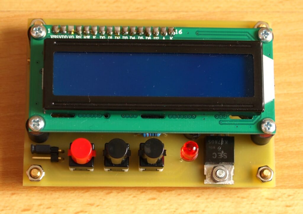
This is a quick project for a timer. Recently I finished my UV light exposure box and thought that it will be convenient to have a build in timer to switch off the light after preset time. So I had a PIC16F628A lying around and after searching the web I found a Brazilian site (I think?) with tons of interesting projects with microcontrolers. This project is based on one of them.

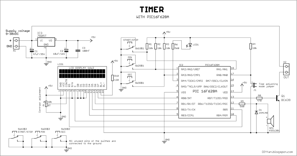
Schematic

Timer_Schematic

There are three buttons to operate the timer: “START/STOP”, “MIN” and “SEC”. “START/STOP” is for starting and pausing the timer. “MIN” is for adjusting the minutes. Minutes may go up to 99 and then starts again from 0. “SEC” is for adjusting the seconds. Seconds goes up to 59 and then starts from 0. “MIN” and “SEC” have repeat functionality. Pressing MIN and SEC buttons simultaneously will reset the timer. When the timer reach 00:00, the buzzer sounds 3 short and 1 long beeps and the LED lights up. The buzzer is electromagnetic type.

After this any of these three buttons will reset the status and LED will switch off. When timer is counting down – RB7 (pin 13) is high and when the timer is stopped – RB7 is low.

With this pin we can operate some external circuitry. In my case there will be connected a transistor which will switch on and off the UV exposure box.

Jumper J1 is for calibrating of the timer. When shorted, the timer enter in adjusting mode. With MIN and SEC buttons we can increase/decrease the value of an internal parameter thus slowing down or speeding up the timer. This value is stored in the EEPROM. Pressing START/STOP button when in this mode will reset this parameter to its default value.

I tested the schematic on the breadboard and everything works as described.

The code is written and compiled with mikroC PRO for PIC. The options for the project are:

  • Oscillator: INTOSC oscillator: I/O function…
  • Oscillator frequency: 4.000000 MHz
  • Watchdog Timer: disabled
  • Power-up Timer: enabled
  • RA5/MCLR/VPP pin function: disabled
  • Brown-out detect: enabled

The .hex file was programmed in the microcontroller with my clone of PICkit2 using “PICkit 2 programmer” v.2.61

Link for downloading the schematic, source .c file and .hex file: Timer (PIC16F628A)

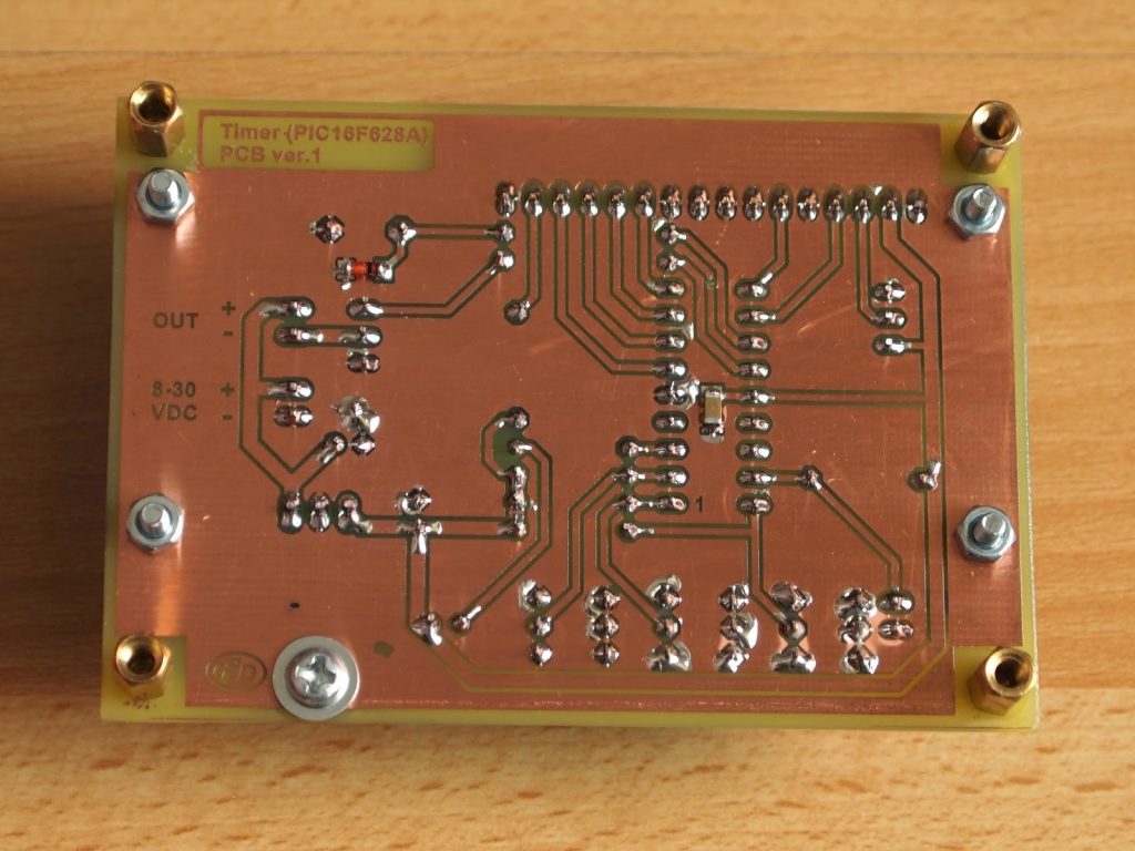
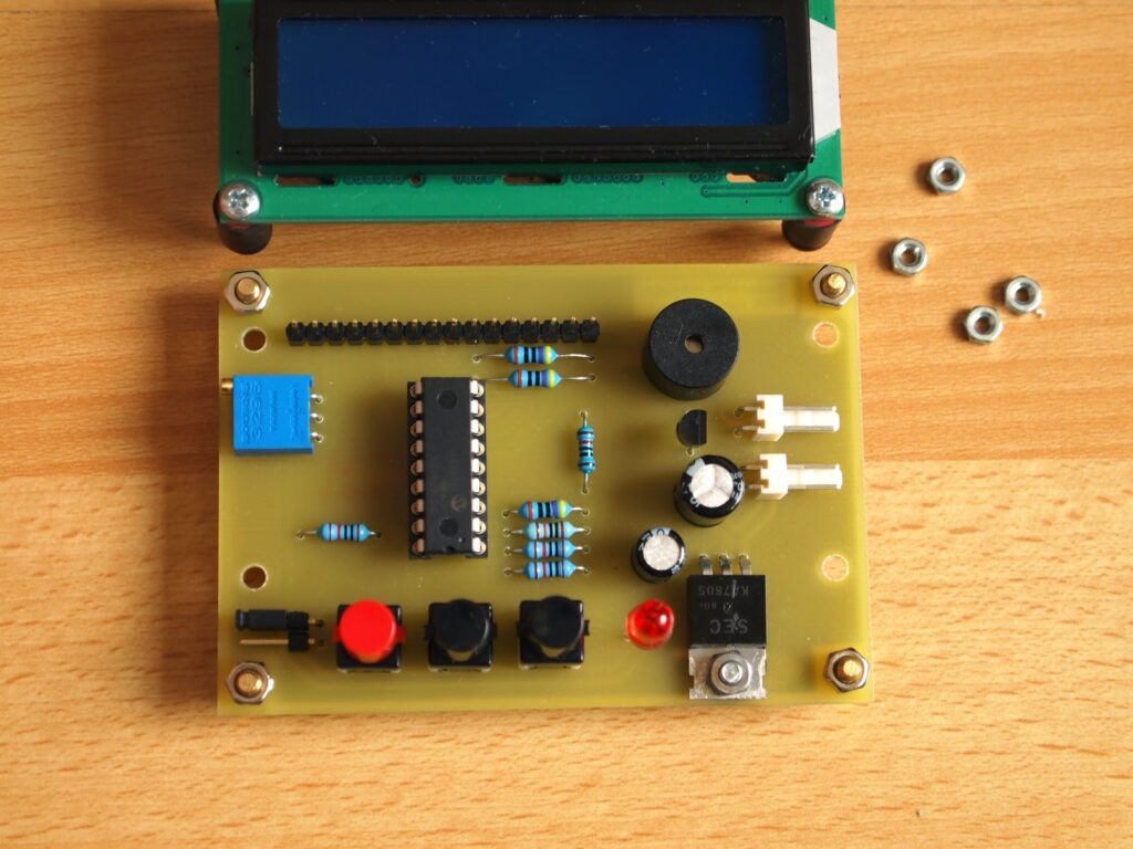
Photos

Timer_photo_(2)

Timer_photo_(3)

USB to Serial Converter using AVR microcontroller

3D_PCB_SMD_first

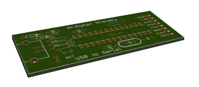
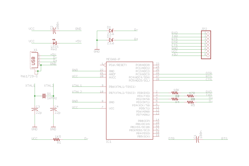
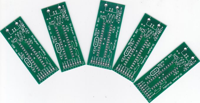
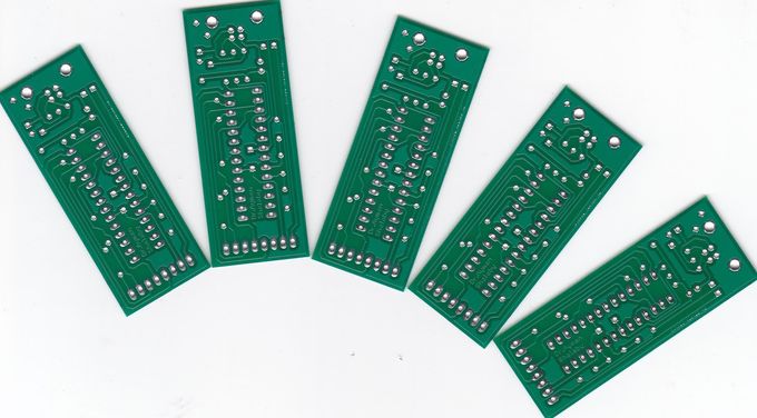
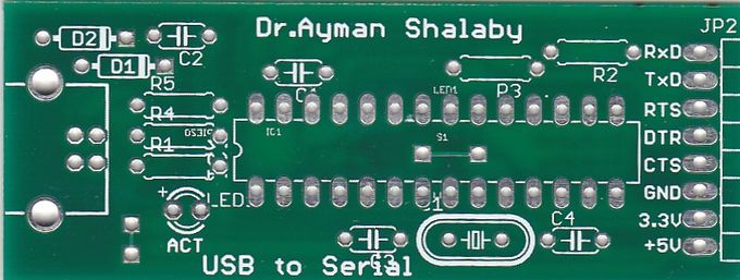
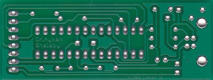
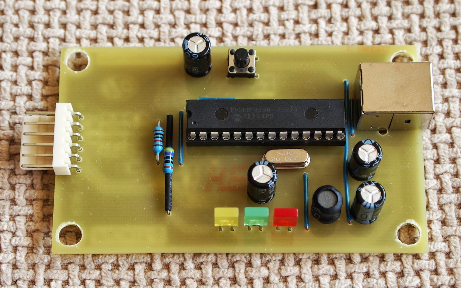
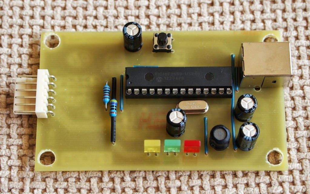
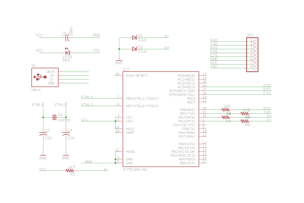
This project is a USB to Serial converter using an ATMEL AVR microcontroller. There are two version of the converter, one with SMD parts and another with TH parts. The mcu used is an ATmega8 and USB communication is done using software on AVR mcu. It’s based on the software USB implementation of AVR-CDC. Firmware can be downloaded from the download section of CDC-RS232.

SMD version

Schematic_SMD

Photos

3D_PCB_SMD (1)

IMG_0006

IMG_0001

Throught hole version

3D_PCB_first

Schematic

IMG_0004

IMG_0005

IMG_0002

IMG_0003

Original PICKIT-2 microcontroller programmer

PICKIT2_2

These days I was thinking about a better PIC programmer that can work with Microchip MPLAB IDE software so that I can write my own programs or edit someone else’s programs. I found that there are numerous versions of the famous Microchip PICkit 2 on the web.

Some of them are using the original schematic published by Microchip and some are lite versions – with different parts or simplified schematics. None of them satisfied my requirements. So I got the original schematic, removed the memory chips and the input ICSP connector (which I didn’t plan to use anyway) and made a new single sided PCB. I used mostly SMD parts.

Schematic

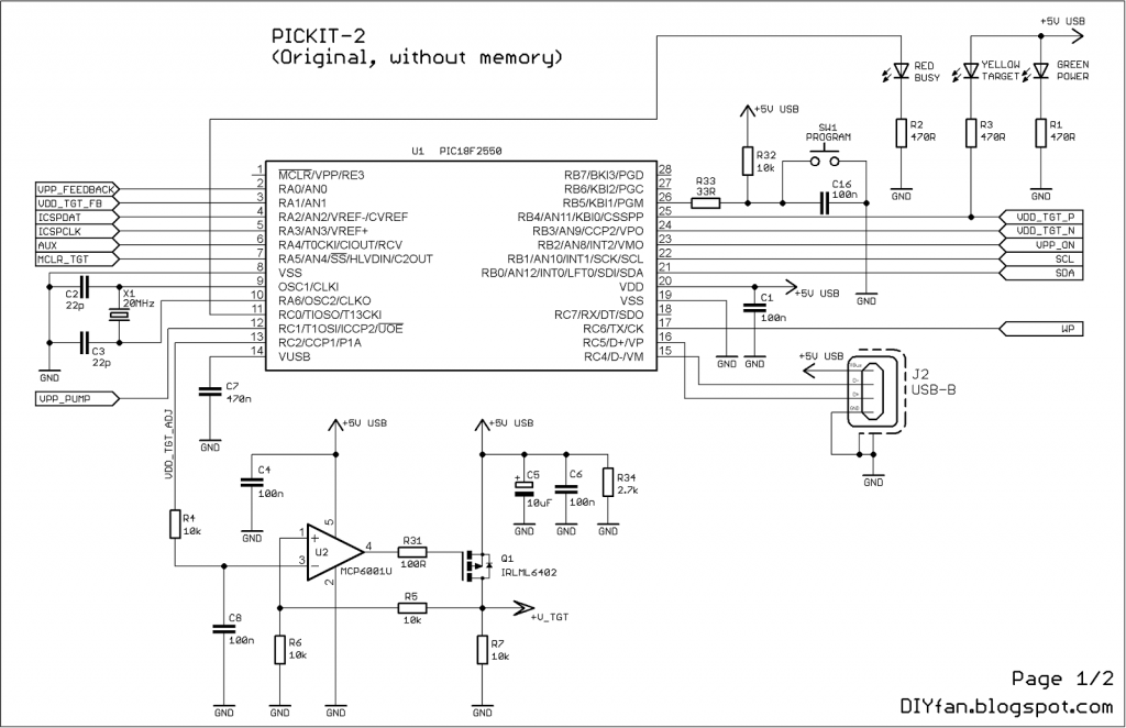
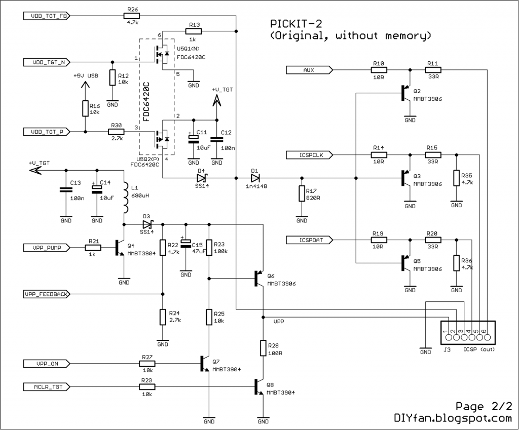
I found out that I can get all parts for the original schematic from local stores, and only two – MCP6001U and FDC6420C – I had to order from Farnel. I also decided to replace two Schottky diodes BAT54 and ZHCS1000 with SS14 because of more convenient package. I programmed the PIC18F2550 microcontroller with my Chinese programmer. Here is the schematic which I used:

PICKIT2_Schematic_1


PICKIT2_Schematic_2

In the end the schematic is not exactly like the original one but it is close enough 🙂 I used the same notifications of the parts like in the original schematic.

PCB

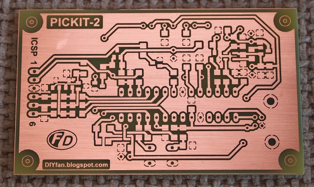
PICKIT2_1

It is one sided and has only five jumpers. The size is comparatively small – 83mm x 52mm.

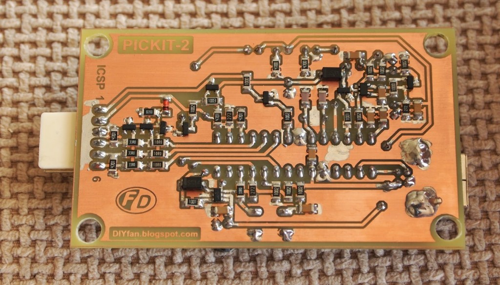
PICKIT2_3

I don’t want to brag, but I think I made the best one sided PCB for PICkit 2 programmer 🙂 . It also works without any hiccups. I tested it with an PIC16F628A which I have at hand. It was recognized in both PICkit 2 software and MPLAB IDE.

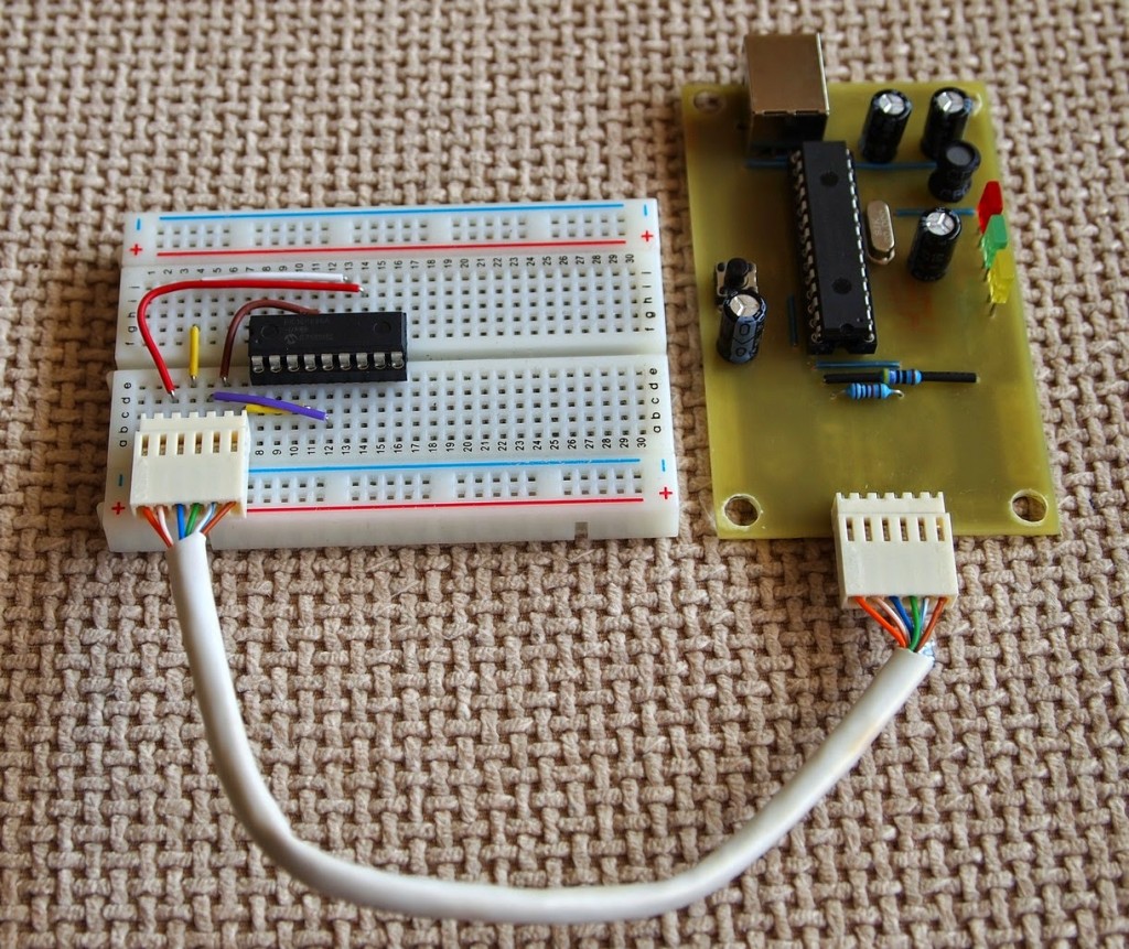
Here is the picture of the programmer connected to the breadboard with the PIC16F628A on it.

PICKIT2_4


8 Opto-isolated Relay board

3D_PCB_th

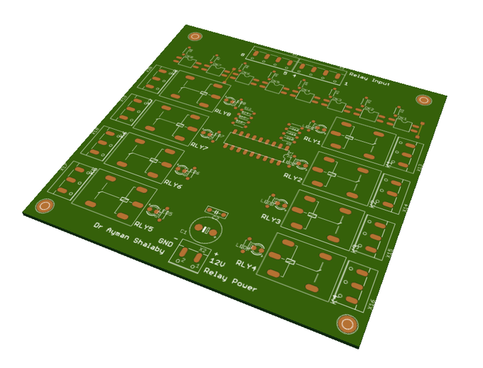
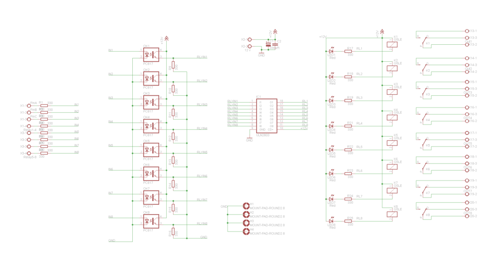
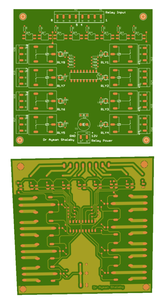
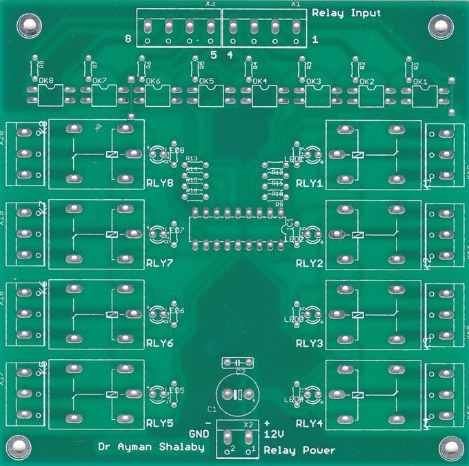
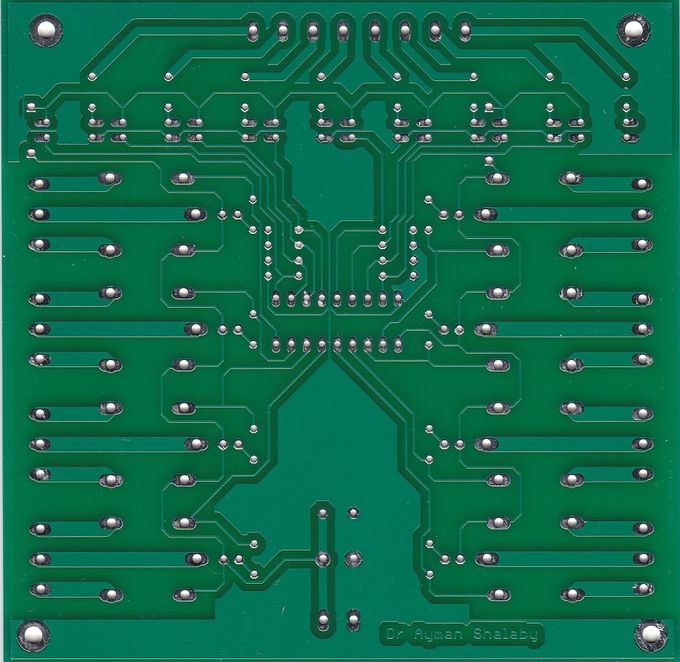
This is a 8 channel relay interface board using ULN2803. All the relays are opto-isolated using optocouplers and can be controlled directly using a microcontroller of any kind (Arduino , 8051, AVR, PIC, DSP, ARM, ARM, MSP430, TTL logic) or a PC.

It’s easy to manufacture and have three pin screw terminals for easy connectivity.

Schematic

The full schematic is shown below

schematic

Photos

3D_PCB (1)

IMG_0001

IMG_0002

TOP PCB Companies