CAN to USB Interface

can-usb


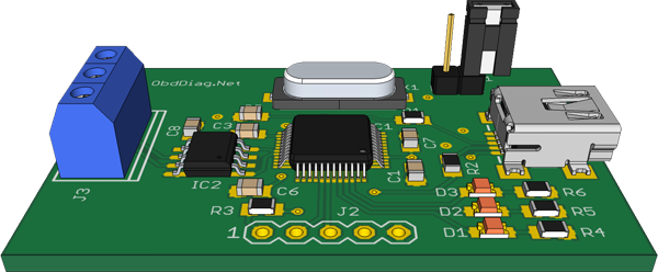
This project started out from a need to build a simple device for monitoring the CAN bus. I choose the NUC140LC1CN 32K Cortex-M0 microprocessor from Nuvoton for major reason – it has both USB and CAN peripherals.

Features

  • Simple design
  • Compatible with the LAWICEL CANUSB protocol
  • Exposing itself as USB FTDI device
  • Supporting CAN 2.0A 11-bit and CAN 2.0B 29-bit frames
  • Has internal FIFO CAN message buffer
  • Self powered from USB port
  • Flash-resident USB mass-storage device (MSD) bootloader for firmware updates
  • Firmware is available for download on the link below

Schematic

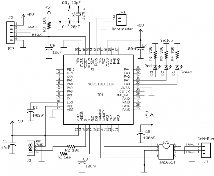
To enable the NUC140 CAN peripheral to communicate with CAN bus a CAN transceiver is required. The TJA1051T chip from NXP solves the purpose. The NUC140 device is capable operating from 5V power supply, there is no need for additional 3.3V voltage regulator. This handy combination makes a simple task implementing the CAN bus interface. There are three status LEDs:

  • D1 is the status of USB connectivity to the host
  • D2 shows the CAN bus activity
  • D3 indicates CAN errors

The NUC140 doesn’t have built-in bootloader and the only way to program it is using ARM Serial Wire Debug (SWD) interface (J2 connector) and Nuvoton ICP programmer. And yes, if bootloader is already pre-programmed it could be activated. That is the purpose of JP1 jumper. Connecting the JP1 before powering the interface will trigger the bootloader.

can-usb-schematic

Bootloader

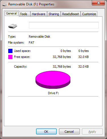
The NUC140LC1 flash memory is divided to two sections, one is for executing user program code (APROM) with the size of 32K and another one for bootloader (LDROM). The LDROM size is only 4K, making a challenge to build a fully-functional USB bootloader. I have used the mass-storage device (MSD) bootloader provided by Nuvoton. Connecting jumper JP1 will start it . As the result a removable drive should be visible in the host file system with a size 32KB. Just copy and paste or drag and drop the CAN-USB firmware update to the bootloader drive. Unplug the USB cable, remove the jumper and plug it in again. The new firmware update should now be running.

usbdrive

Programming the CAN-USB Interface and NuTiny-SDK-140

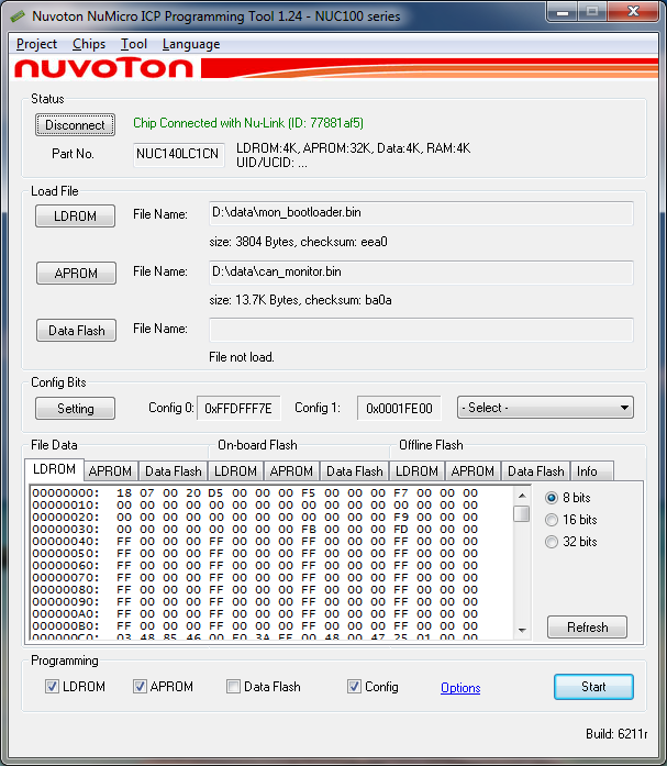
Programming the NUC140 processor requires Nuvoton’s Nu-Link programmer and Nuvoton ICP programming application. Instead, I decided to use the NUC140 demo board (NuTiny-SDK-140) available from Digi-Key. It has the two parts, the part with NUC140 chip and Nu-Link programmer itself. The board is even perforated to detach the Nu-Link part. Actually, you can build this device solely around NuTiny-SDK-140 demo board, the only additional CAN transceiver chip will be required.

NuTiny-SDK-NUC140


With Nu-Link connected the programming NUC140 is not complicated. The key issue here is to choose loading from LDROM instead of APROM (in Config settings) to have the USB bootloader functionality.

Nu-Link

The Software

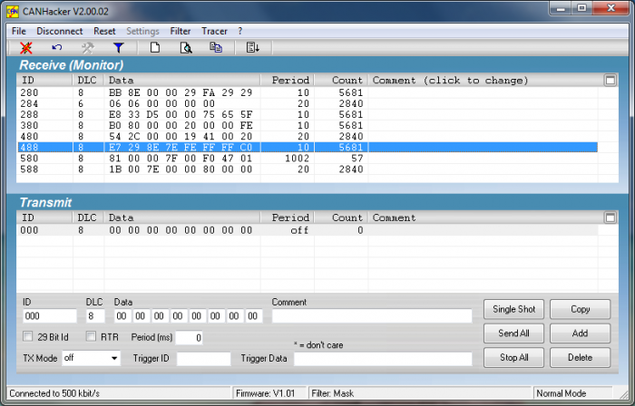
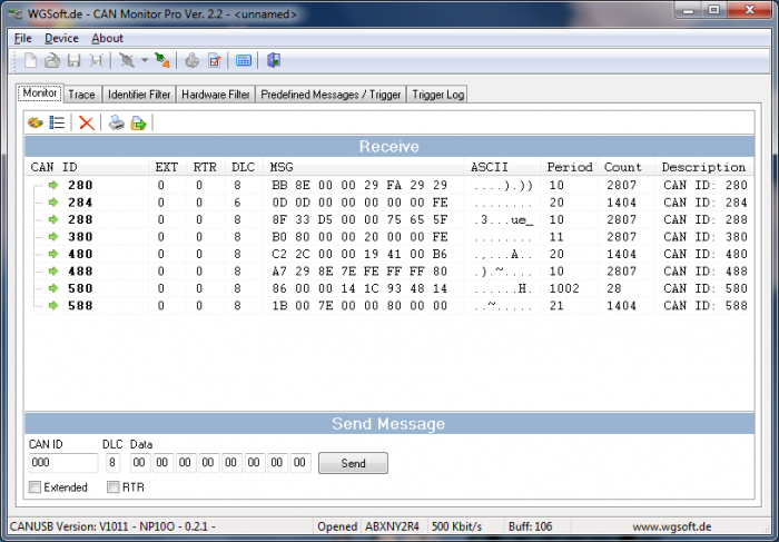
The CAN-USB interface is compatible with LAWICEL CANUSB protocol and it will work with the applications built for it. The are two application I have tested with the CAN-USB interface:

CANHacker V2.00.02

The CANHacker application is freeware. I was unable to find the manual for it, but using it is simple and straightforward.

canhacker

CAN Monitor Pro V2.2

This application is made by wgsoft.de. Note, that the site is mostly in German.

can-monitor-pro

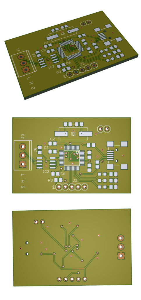
PCB Design
3D_PCB


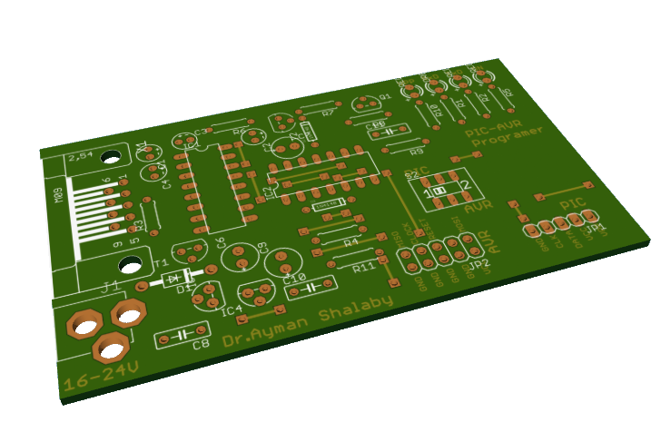
Serial AVR and PIC programmer

3D_PCB_top_first

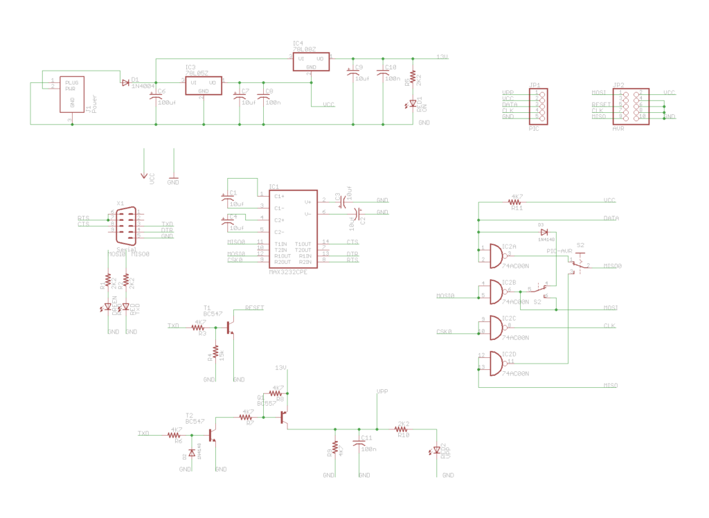
This is a dual MCU programmer which supports both AVR and PIC mcu and there is a switch to select between them.

It’s easy to manufacture and have only through hole parts.

Features

  • RS232 Serial interface
  • AC-DC powered
  • MAX232 interface
  • standard programming sockets for PIC and AVR
  • easy to build, all component are TH parts
  • 74CA00 for protection
  • LED indicators for VPP, TxD, RxD, Power
  • Compatible with PonyProg and similar software
  • 10 Pin ICSP for AVR (Miso, SCK, Mosi, Reset, GND, VCC)
  • 5 Pin ICSP for PIC (VPP, VDD, VSS, PGD, PGC)

Schematic

The full schematic is shown below:

schematic

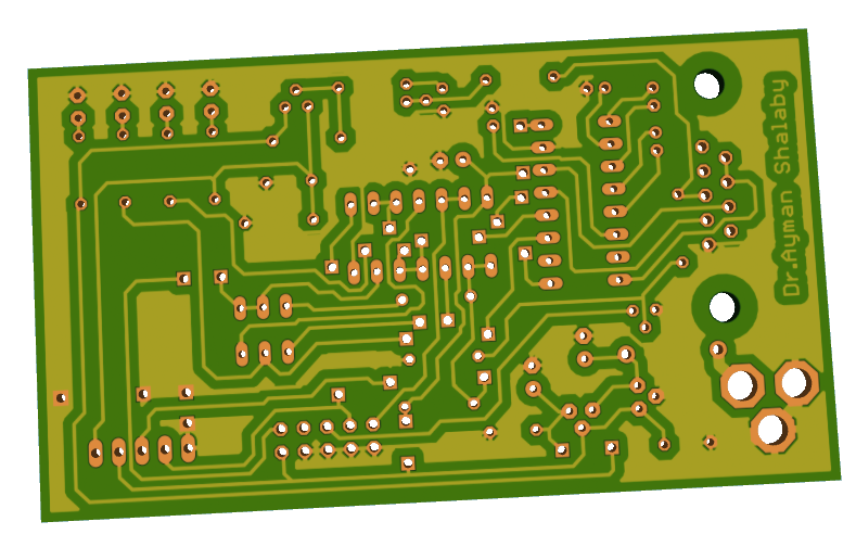
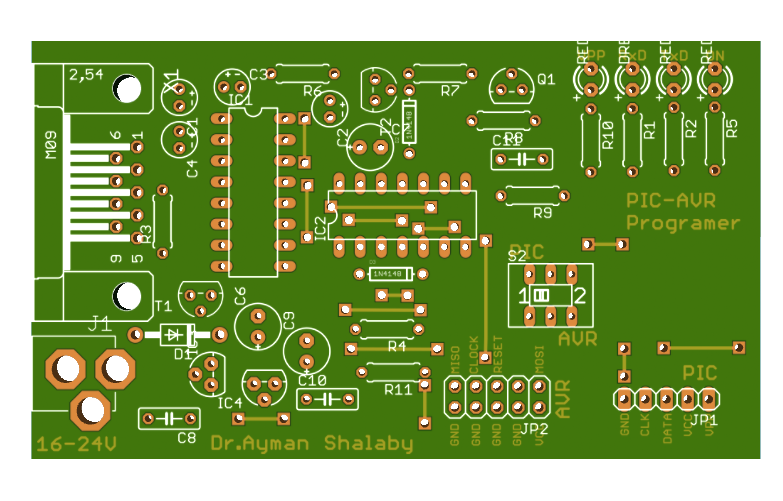
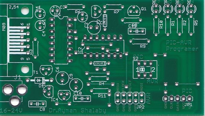
PCB Design
3D_PCB_bottom

3D_PCB_top

IMG_0001

IMG_0002


EGYDuino – Arduino compatible board

3D_PCB_EgyDuino

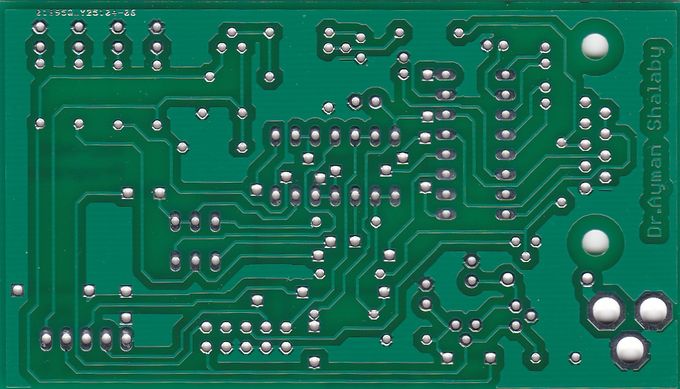
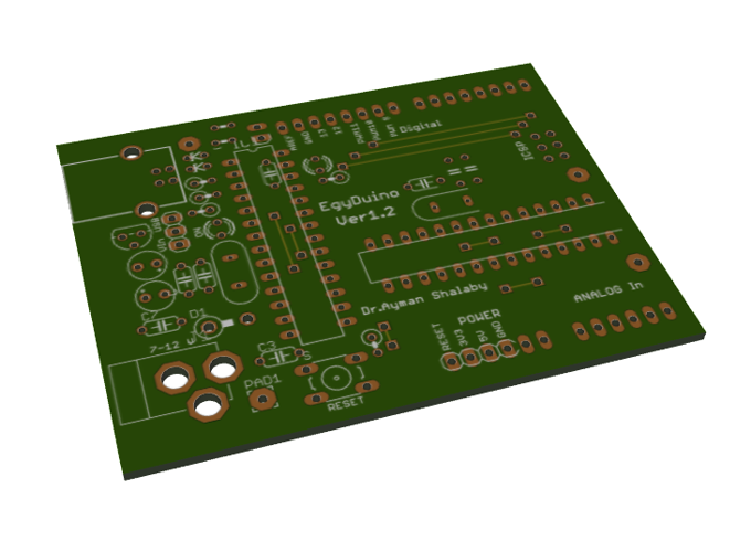
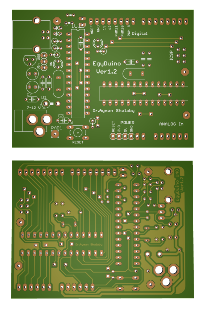
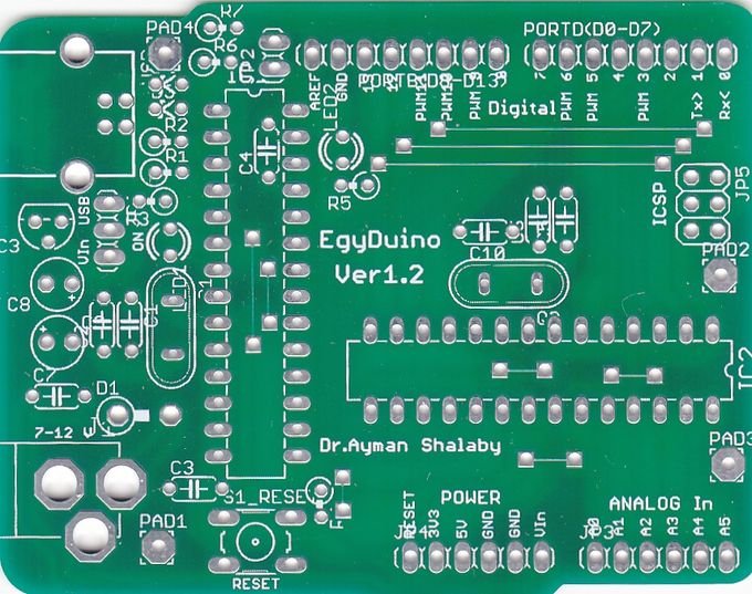
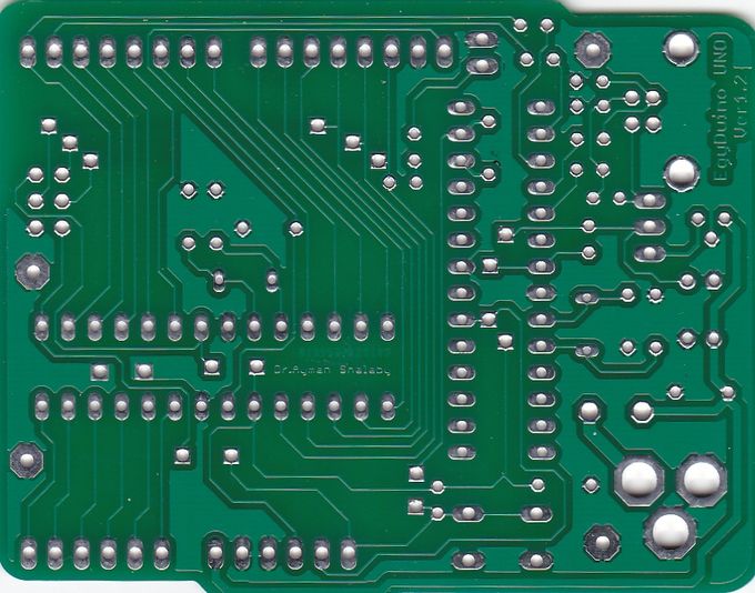
EGYDuino is a DIY Arduino clone made on a single sided PCB board. It’s simple and cheap to build using home PCB fabrication methods and it’s 100% compatible with Arduino.

Description

ATmega8 takes care of the USB to serial communication and should be burned with AVR-CDC232 firmware. AVR-CDC creates a virtual COM port on the PC after connecting the device and installing the appropriate driver. The ATmega 8,168 should be programmed with ArduinoNG boatloader. This can be done through another Arduino board (set a ISP programmer) using the Arduino IDE or by using a separate programmer (USB, serial or parallel) like USBasp with suitable software. Also you can use Arduino Duemilanove bootloader for ATmega 168 or 328.  The features of this board are:

  • It’s using ATmega8 as interface IC
  • Has USB connection to PC
  • Standard RESET button
  • 100% compatible Arduino PINs
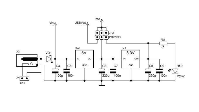
  • 5V regulator
  • 3.3V output
  • compatible size and design
  • All component are TH (through hole) parts
  • USB or DC power switch
  • LED  for PIN13 with Jumper
  • LED for power
  • ICSP PINs
  • easy to build
  • ATmega8,168,328 core using arduinoNG
  • standard DC power jack

EGYDuino can be powered via the USB connector, or with a voltage regulator through an external adapter.

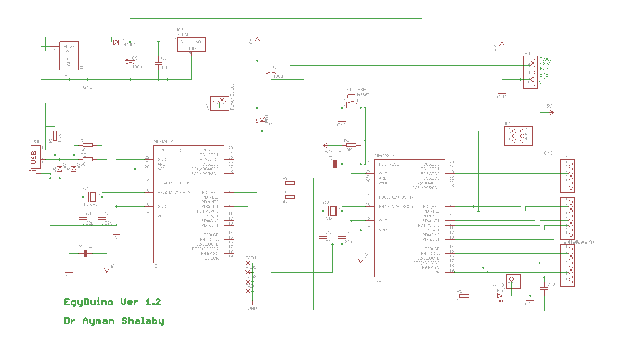
Schematic

The full schematic is shown below

Photos

3D_PCB_rendering

IMG_0001

IMG_0002

ATmega64 Development Board

3D_rendering_2

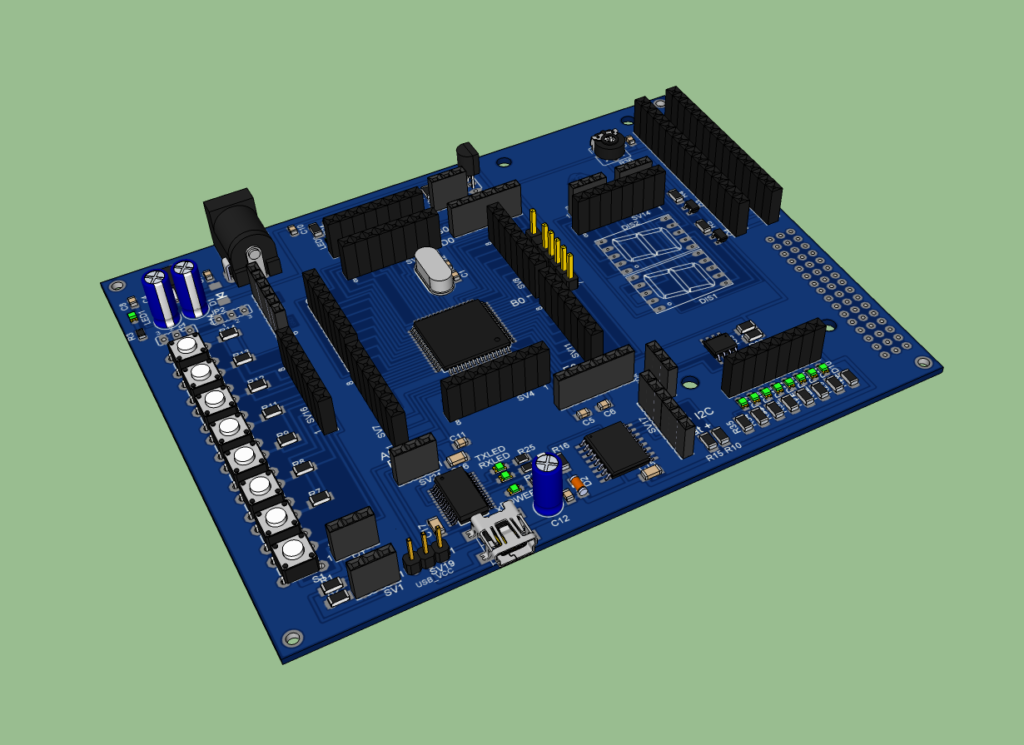
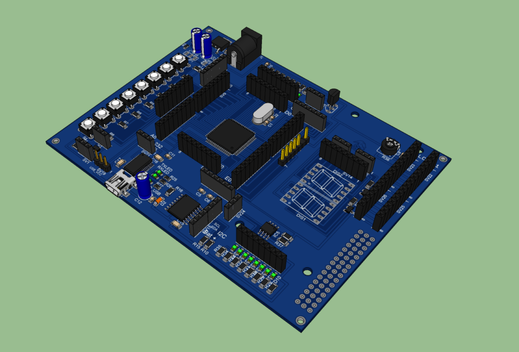
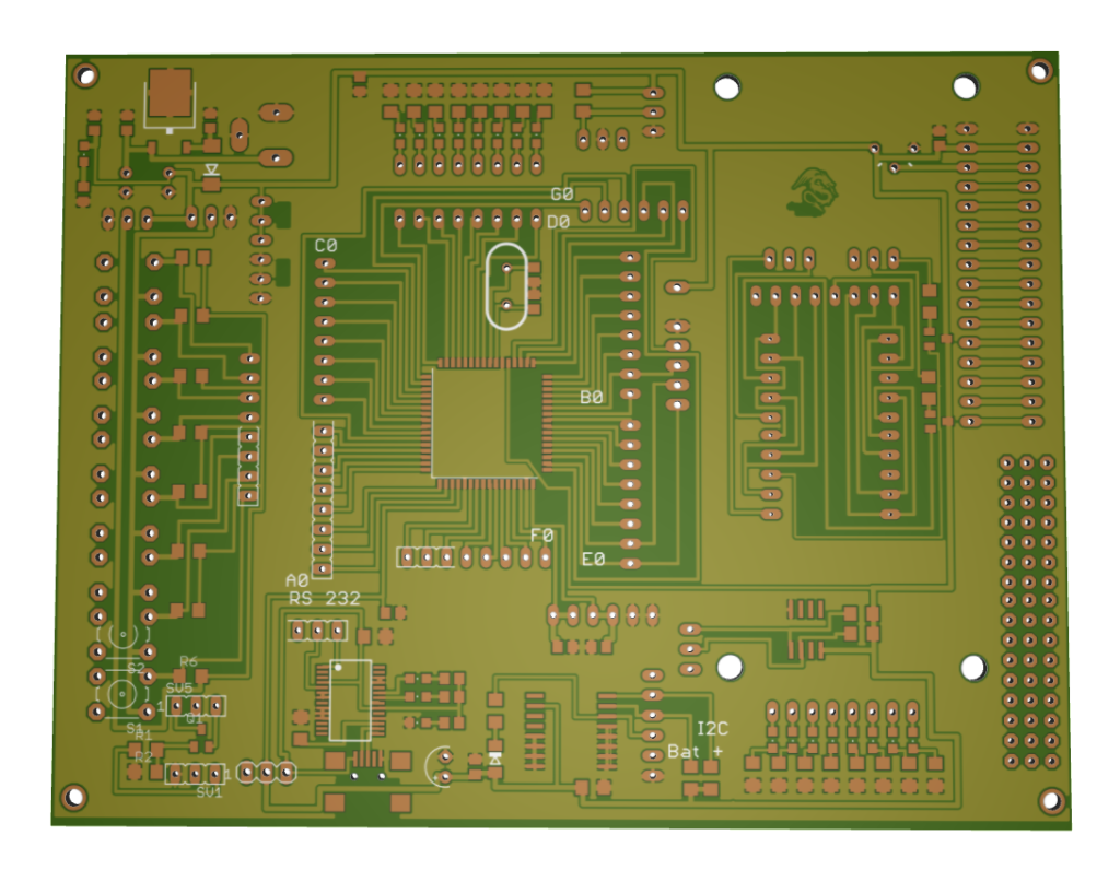
This project is a development board for Atmel ATmega64 microcontroller and can be used to easily develop custom AVR firmware or as an introduction board to microprocessors and programming. A development board is better to be used instead of a breadboard setup as it facilitates the connection of the different components using PCB headers. The project was designed at the time when the Arduino board wasn’t available in the Czech Republic and is equipped with different modules.

Description

The features of this board are:

  • Atmega64 – all the ports available through pins, a different crystal can be connected (optional frequency crystal)
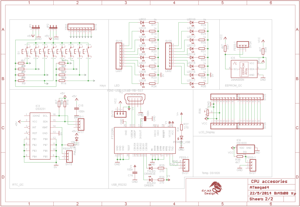
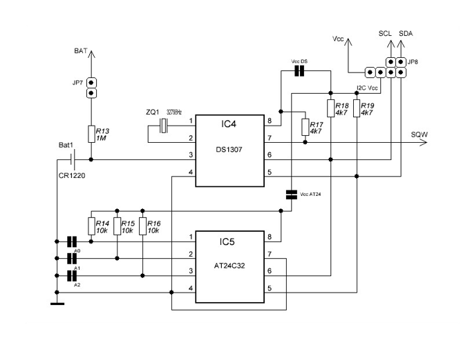
  • DS3231 RTC, real-time IC / I2C
  • Temp. DS1820 1wire Temp. sensor
  • EEPROM 24AA00SN / I2C EEPROM
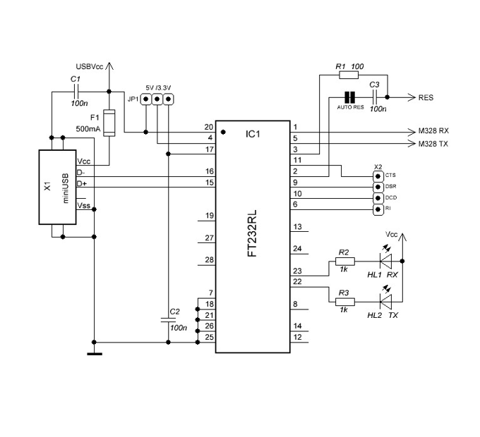
  • USB Port FT232RL USB/RS232 converter
  • Buttons 8x -16x LED
  • Connect LCD Display 16×2
  • 7segment-LED Display
  • N-FET For PWM
  • ISP Programming connector

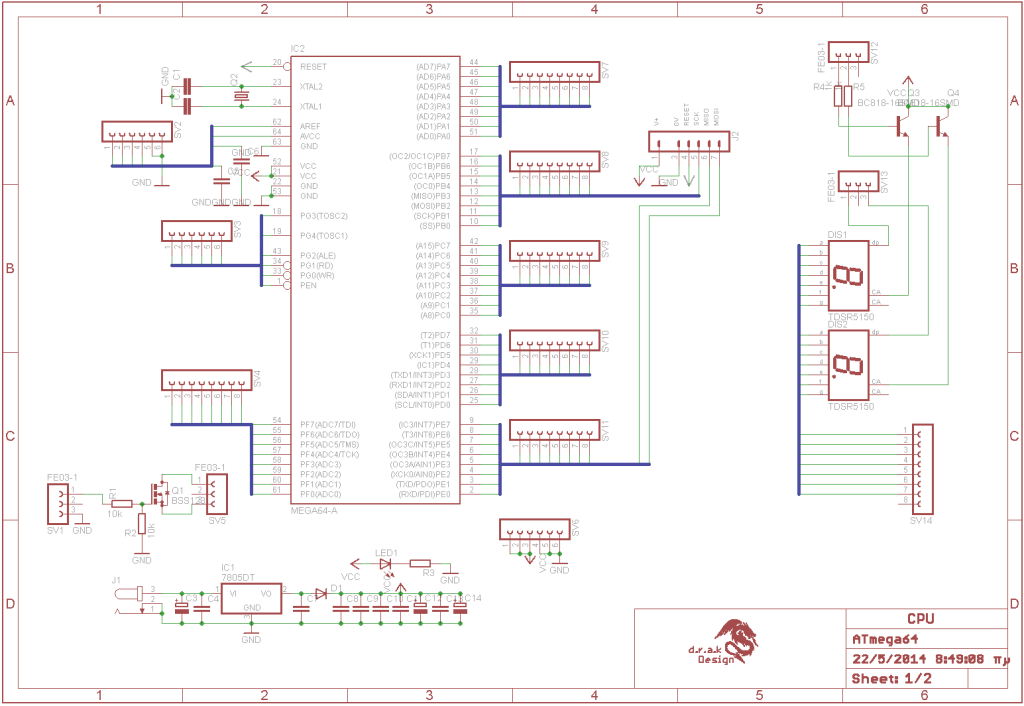
All module pins are labeled for easy connection with the processor and there are separate connectors and jumpers for all MCU ports so you can easily connect, test and debug your firmware. Also there is an ISP programming connector J2.

The PCB can be powered via the USB connector, or with a voltage regulator through an external adapter.

Schematic

The full schematic is shown below

schematic_1

schematic_2

Photos

3D_rendering_1

3D_PCB

miniLOG – Precision Standalone Voltage Logger

3D_minilog_front

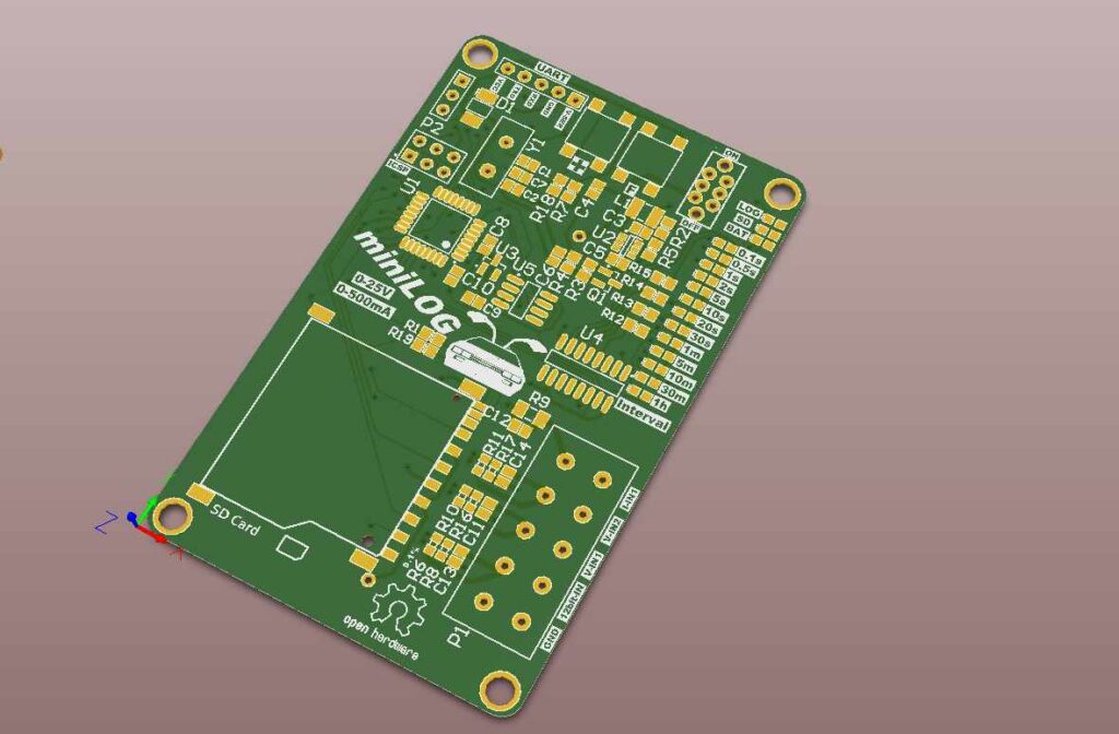
miniLOG is a precise standalone voltage logger that save the data on a SD card. It has 4 basic analog channels:

  •  one has 12bit resolution for voltage measurements,
  • two channels have 10bit resolution for voltage measurements and
  • one channel has 10 bit resolution for current measurements.

Input voltage range is 0-25V and current range is 0-500mA. The data are written on a simple .txt file on SD card and can be further proccessed using spreadsheet software.

Description

This is my latest project called miniLOG. It’s a basic data logger designed to have similar functionality to a data logging mode on some expensive $300+ multimeters for a fraction of the cost.  It has four basic channels: a high resolution 12-bit voltage measurement channel with an MCP3201 ADC, two 10-bit voltage measurement and a 10-bit current measurement channel. It’s capable of measuring voltage from 0 to 25V (with 0.0061V steps on the 12-bit channel and 0.025V steps on the 10-bit channels) and current from 0 to 500mA.

The miniLOG logs the readings onto an SD card which you can later plug into your computer, import the .txt file to a spreadsheet software like MS Excel and make graphs, charts etc.

AVR microcontroller

mcu_schematic

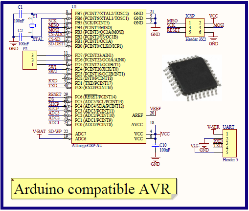
The miniLOG is based on ATmega328P-AU microcontroller in the TQFP32 package. It’s Arduino compatible so you can easily modify the code. It’s accompanied by a 16MHz crystal oscillator to reproduce the Arduino UNO circuit. You probably could get by without the crystal but since the entire Arduino bootloader operates based on that 16MHz crystal it’s a good idea to keep it. Also the miniLOG uses SPI interface to communicate with the ADC and the SD card so a little bit more clock accuracy is a good thing to have.

sd_card_schematic

You can probably notice the 5 pin header. Its purpose is to connect to an external UART module like for instance a USB-UART or bluetooth-UART module. With a bit of extra code you can communicate with the miniLOG using USB or bluetooth. These modules are really cheap (~5 USD on eBay).

Analog to digital converter

analog_schematic_th

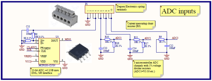
After a lot of research I decided to use the Microchip MCP3201 ADC. It’s a precise, low-power 12 bit ADC. The current measuring channel is basically the same as the others, it just uses a 1% 1ohm 500mW current shunt resistor. The miniLOG measures voltage across the 1ohm resistor. The safe maximum current is 500mA, although technically you could put up to 700mA through it. All voltage channels have voltage dividers dividing the input voltage by 10. Since the reference voltage in the circuit is 2.5V the maximum voltage onthese channels is 25V. The 12-bit channel requires something more precise, that’s why I used 0.1% resistors on that one.

Analog circuitry

analog_circuit_schematic

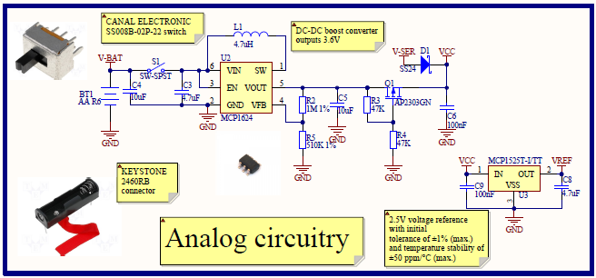
The miniLOG is powered by an AA battery. It’s connected with the main power switch to anMCP1624 DC-DC boost converter, which outputs 3.6V required by the rest of the circuit. The V-SER net is the voltage from the serial connector. If for example you want to power the miniLOG from a USB-UART module, two SS22 Schottky diodes and a P-channel MOSFET take care of it so the AA battery can’t burst into flames.

The voltage reference is an MCP1525, a 2.5V reference with 27 ppm/°C typical voltage drift. I decided to go for a convenient SOT-23 package for this one.

User interface

user_int_schematic

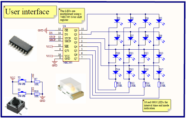
The user interface comes down to basic mode, channel and interval time selection. The user controls the miniLOG with two humble microswitches. The interval time and chosen mode is displayed using 16 0603 LEDs controlled by the 74HC595 8 bit shift register. It may seem silly to use 16 LEDs, but I have actually given it a lot of thought, took into account DIP switches, 7 segment displays, but this was by far the best solution.

Schematic

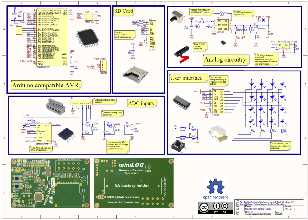
The full schematic is show below

schematic

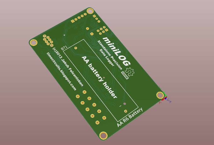
Photos

3D_minilog_back_th

Buy miniLOG

The project is still at the prototype stage but should be available to buy in a couple of months.

Serial 4-digit seven segment LED display

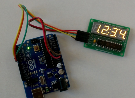
photo_1

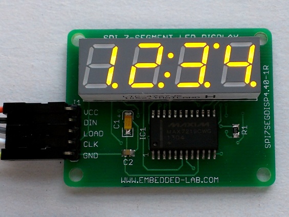
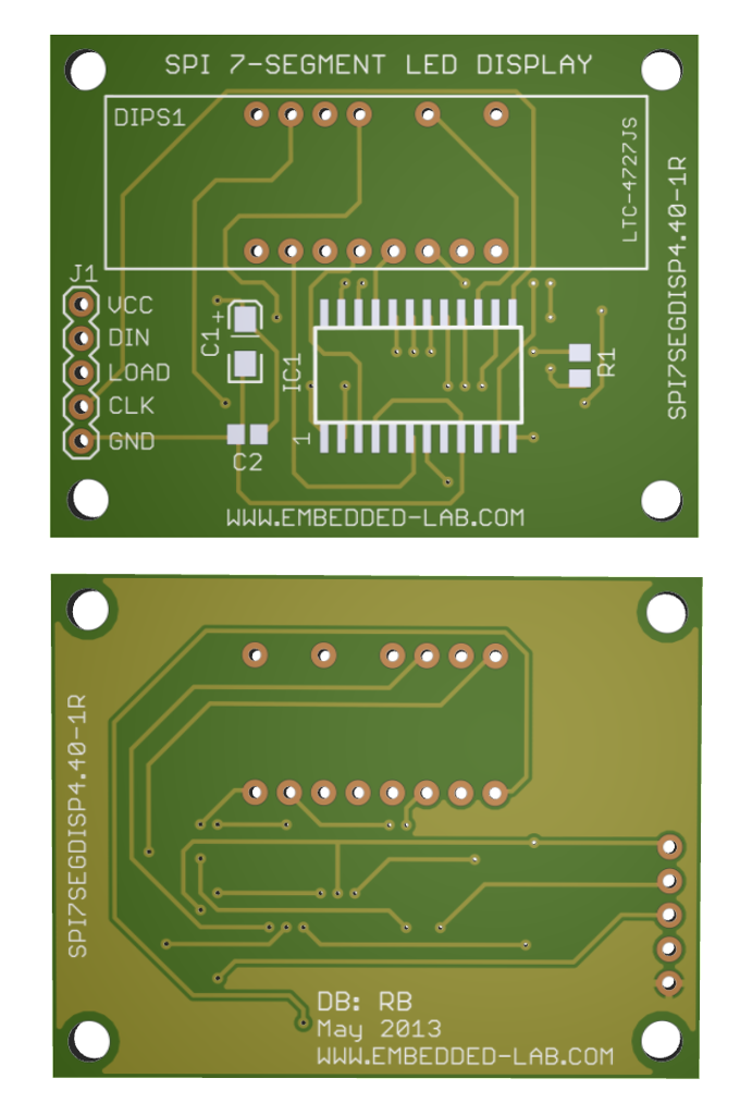
This project is a 7 segment LED display module that can be driven using SPI protocol, so it needs only 3 pins of your mcu to drive 4 x LED displays. It’s based on MAX7219 LED display driver.

Description

Seven segment LED displays are very popular for displaying numeric information because they are very attractive and readable from a far distance and wider viewing angle.

The downside is they are resource-hungry. For example, it requires 12 I/O pins of a MCU to drive a 4-digit seven segment display using a standard time-division multiplexing technique.

Here I present a serial seven segment LED display module that can be used with any MCU using a 3-wire SPI interface. This particular display has four digits (0.40” size) and two colon segments (to support time display) display.

Schematic

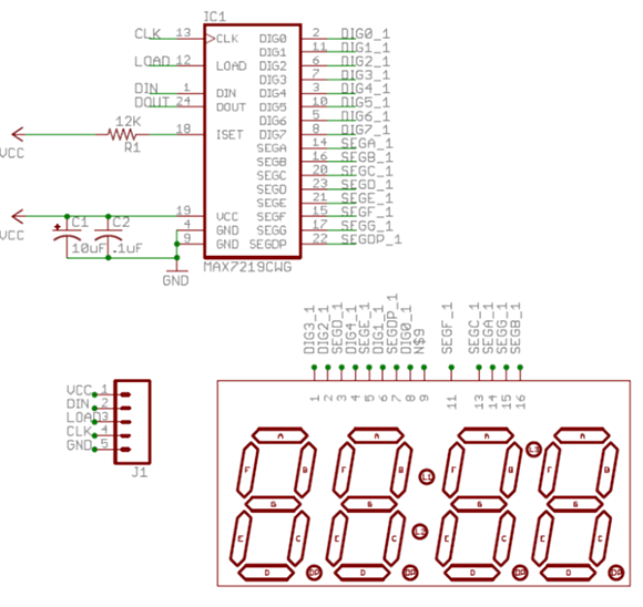
he main controller of this display module is MAXIM’s MAX7219 driver chip. Included on-chip are a BCD decoder, multiplex scan circuitry, segment and digit drivers, an 8×8 static RAM to store the digit values, and a 3-pin SPI interface to receive the display data from the host MCU.

The segment current for all LEDs is set through only one external resistor. However, the device also provides a digital control of the display brightness (16 steps from minimum to maximum) through an internal pulse-width modulator.

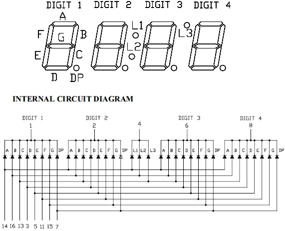
The seven segment module used in this project is LITE-ON, Inc.’s LTC-4727JS module, which has LED segment arrangement and pin configuration as shown in figure below.

7Segments_displays

The interface between MAX7219 and the LTC-4727JS LED module is shown below. The common cathode terminals (Digit 1, Digit 2, Digit 3, and Digit 4) of LTC-4727JS are connected to D3, D2, D1, and D0 pins of MAX7219 driver chip, respectively. The common cathode pin (4) of L1, L2, and L3 LED segments goes to D4 pin of MAX7219. So, in order to turn on L1, L2, and L3 segments, D4 digit select pin of MAX7219 should be active. The display is powered with 5V applied to its VCC pin. Resistor R1 defines the constant current through the LED segments.

schematic

Parts List

parts

Interface Example

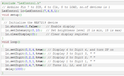
This display module can be easily interfaced with Arduino using the LedControl library. Here’s an example that displays numbers 1 through 4 and activates the L1, L2, and L3 segments. The SPI interface pins DIN, CLK, and LOAD of MAX7219 are driven by Arduino digital I/O pins 7, 6, and 5 respectively in this example. However, the LedControl library allows customization of these pins.

code

Photos

3D_PCB

photo_2

References

DigiPot – Rotary Encoder Digital Potentiometer

SAMSUNG

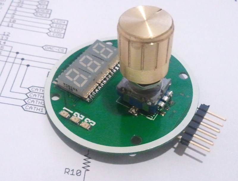
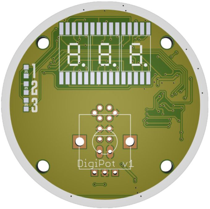
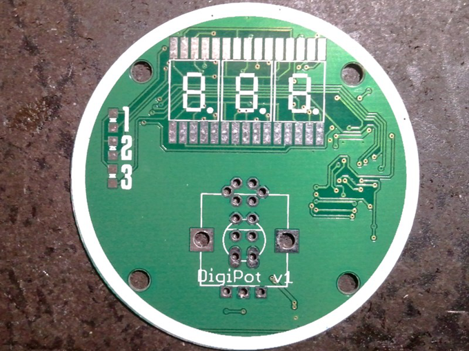
DigiPot is a digital potentiometer using a rotary encoder as input along with a 7 segment display that show the current pot value.

Description

The “potentiometer” is actually a rotary encoder (TW-700198) connected to a microcontroller that reads the signal from it and convert it to a value that is displayed on 7-segment displays. The value also is sent via i2c/spi/serial/usb to the host. Also 3 LED and included for status indication.

The board is planned to either be operated in an autonomous mode where the display is updated by the board itself or in a host mode where the host is telling the board what to display.

.: source code isn’t available yet :.

A “Rotary Encoder” aka “Quadrature Encoder” is sending pulses to the microcontroller that will determine how the user is turnin the knob and calculating a current value for it. This value will be digitally sent to the host via i2c or another serial protocol. At the same time an analogue voltage will be generated and be presented at a output.

Possibly also the value could be sent to a digital potentiometer chip like a MCP4551 as well to set a resistive value.

An ATmega8/168/328 is selected as the microcontroller since it has enough i/o for this project. I also choose to use a ISPtouch connector for as the programming interface.http://dangerousprototypes.com/?p=62605

Specifications:

  • Three digits display with movable decimal point.
  • Three status leds.
  • Quadrature encoder with button-functionality.
  • Communicate with host via i2c/serial-ttl.
  • Multiple units can be chained.
  • The value can be output as an analogue voltage with 12 bit resolution.

Parts description

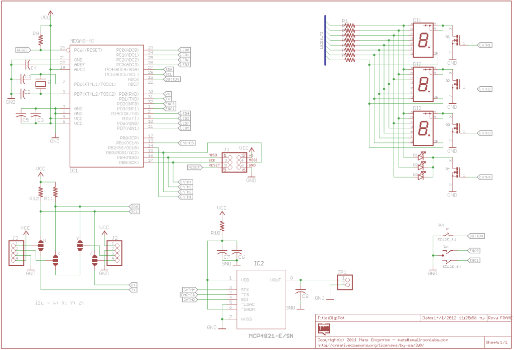
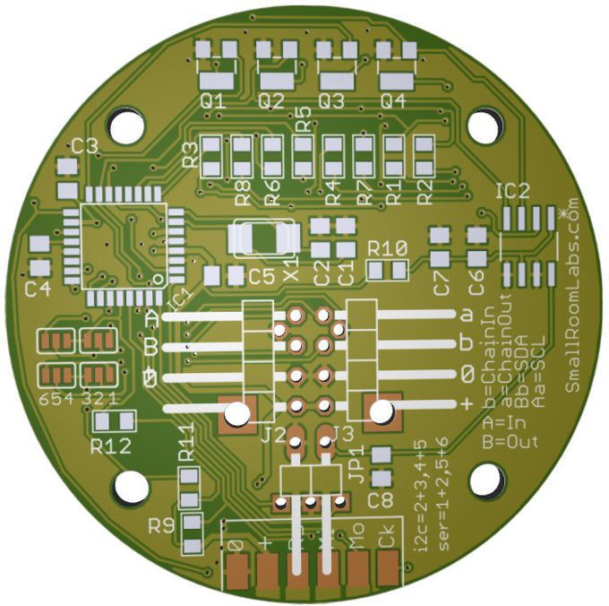
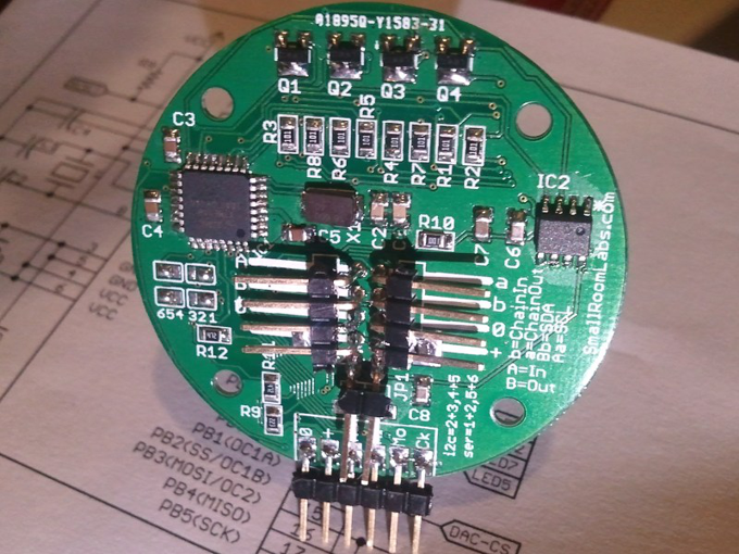
Starting from top there’s 4 n-fet transistors for muxing the cathodes of the displays and leds. Then there are 8 anode resisors. The atmega with C3/C4/C5 decoupling caps. The crystal with C1/C2 load caps is followed by R10/C7/C6 that is a filter for the supply to the mcp4821 12 bit dac.

Below the atmega there are some jumper for selecting if the units is to communicate with serial uart or i2c. The two 4 pin headers can be used to chain multiple units either by i2c as a bus, or a daisy-chain with serial, if serial the last unit in the chain must be looped.

R9/R11/R12 is pullups for i2c and reset. The 2-pin header is analogue voltage out and is filtered by C8. The 5 pads on the bottom is the programming header.

Schematic

schematic

Photos

3D_pcb_front

3D_pcb_back

PCB_photo_0_th

PCB_photo_2_th

BO.Duino – ATmega328 Arduino Compatible board

IMG_0114

BO.Duino

Description

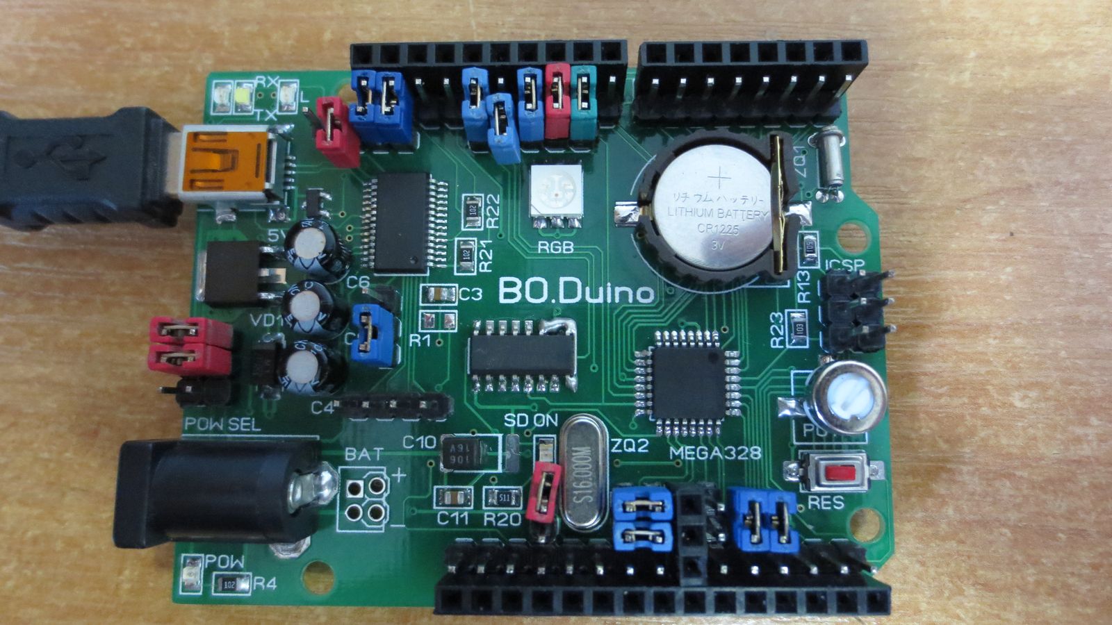
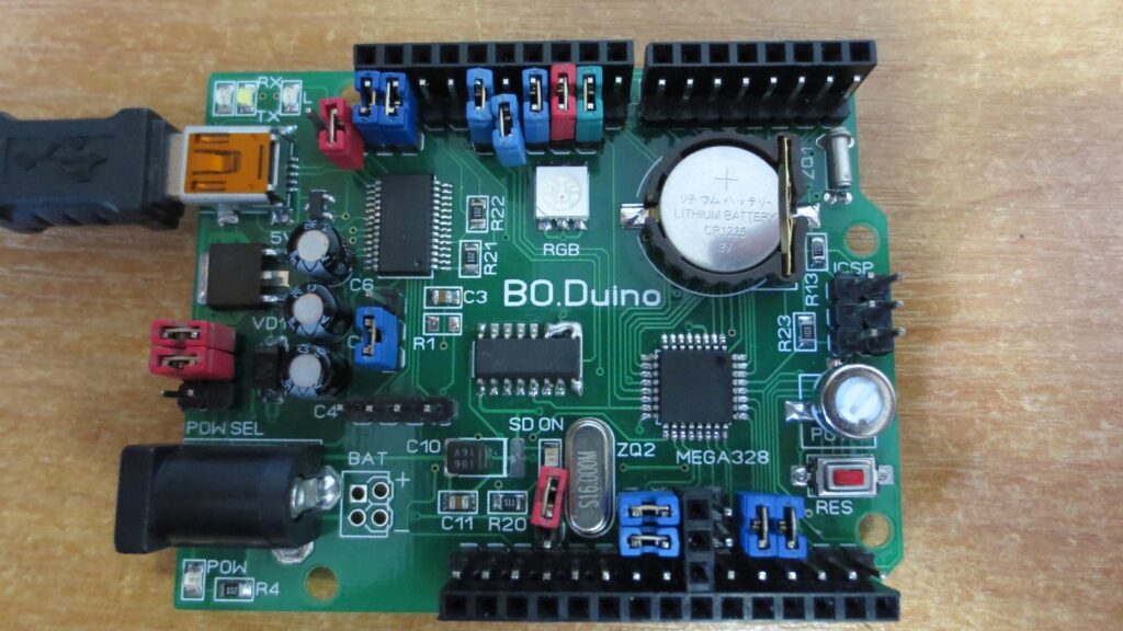
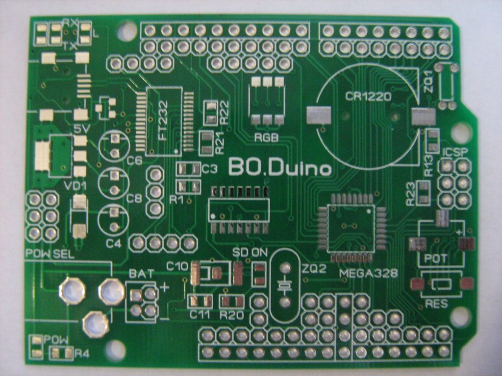
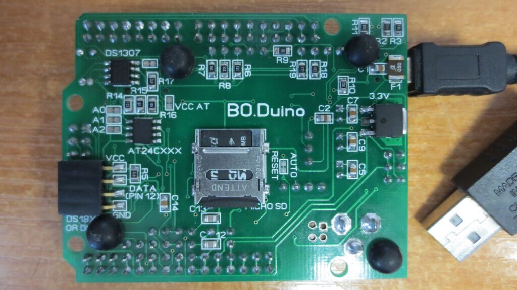
BO.Duino is an Arduino compatible board based on ATmega328 ATMEL’s mcu. This board features many peripherals usually externally connected on a breadboard or prototyping board such as sensors, SD card etc. Peripherals included are:

  • A real-time clock
  • AT24 series external memory chip
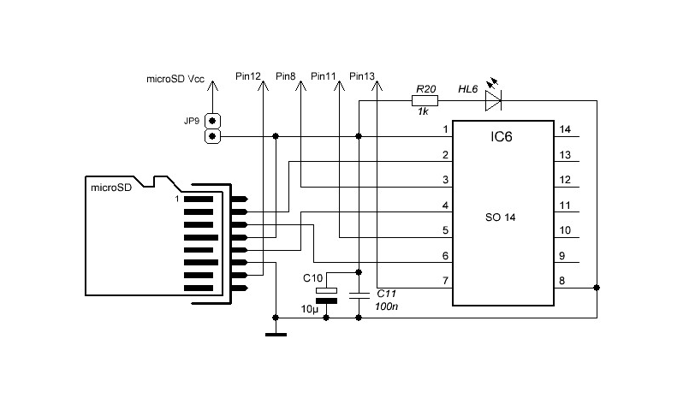
  • MicroSD card adaptor (SPI)
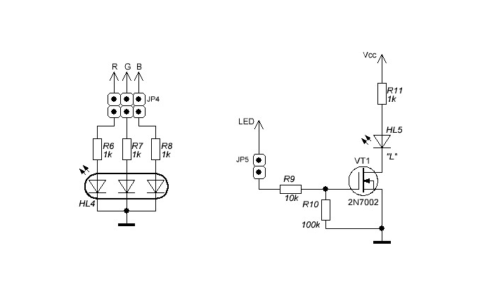
  • RGB LED
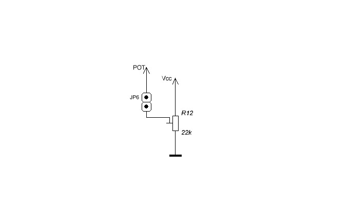
  • A potentiometer on analog input
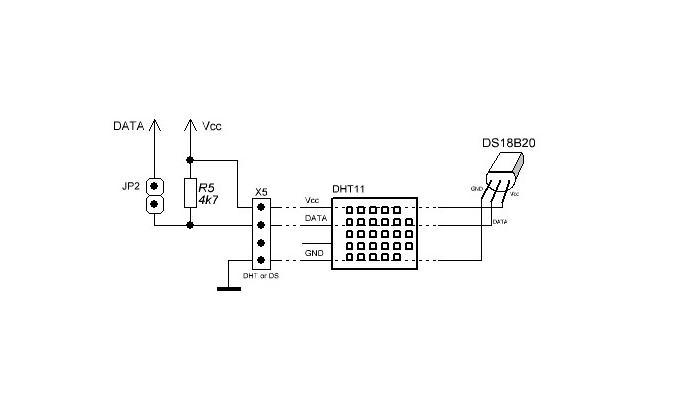
  • Connector for DS18b20  or DHt11  series sensors

The board should be configured as Arduino Duemilanova on Arduino IDE. A jumper is used to select the FT232 chip output level. Also the board’s power supply is selected manually. The FT232RL enables you to programm a new firmware or change the bootloader without the need of extrernal programmer .

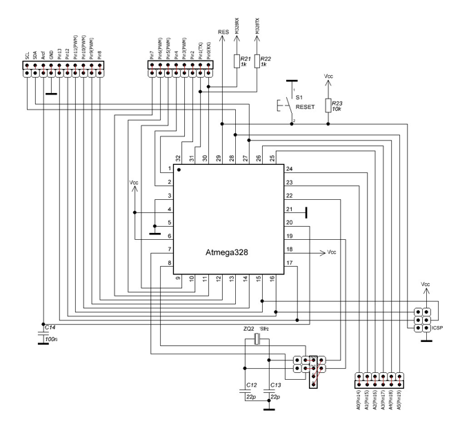
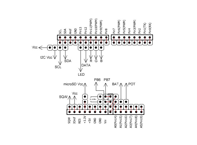
Schematic

schematic_1_th

schematic_2

schematic_3

schematic_4

schematic_5

schematic_6

schematic_7

schematic_8

schematic_9

Photos

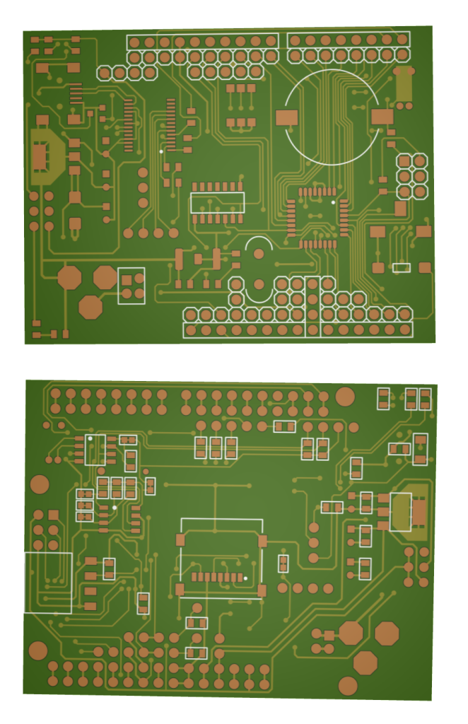
3D_PCB

IMG_0650

IMG_0117

Automatic School Bell

schematic

Description

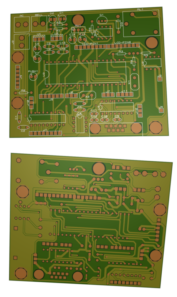
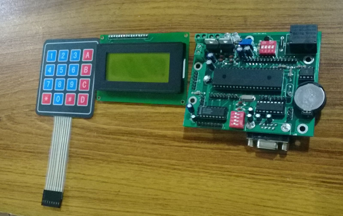
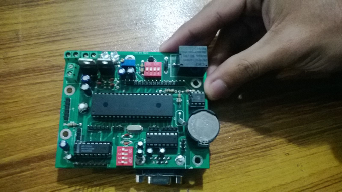
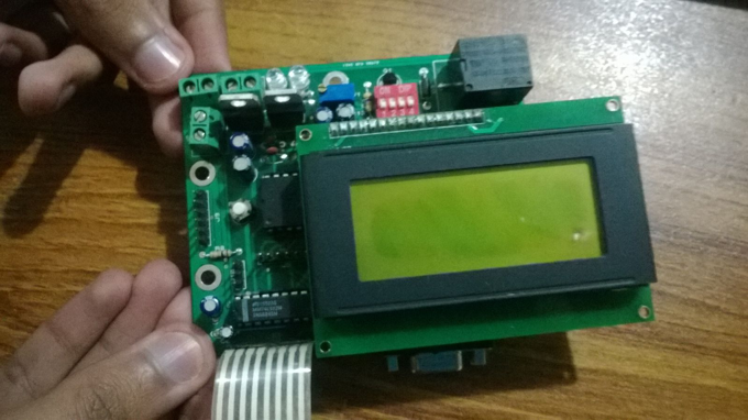
This project is an Automatic School bell system. Such a system triggers a bell (or operates any other load) at predifined time. In this version some advanced features are introduced:

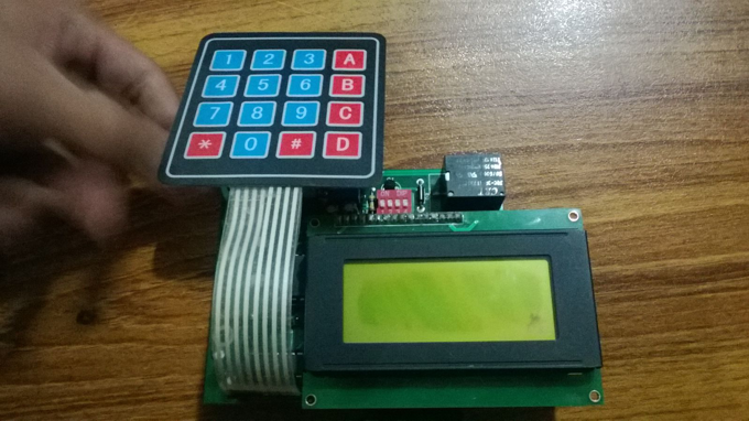
  • 16×2 LCD Display ( Displays current date, time and day)
  • 4×4 Keypad for Inputs
  • Stand alone product ( no PC required to program or maintain ringing schedule)
  • No battery required to maintain clock and ringing schedule
  • Variable ringing time
  • Max 10 bells can be set
  • Custom Weekend filters
  • Monthly OFF / Weekly OFF
  • Half Day
  • Total AC Power Handling : 1000W (240V 5A)
  • Connect as many AC electronic bells in parallel form
  • Built-in back up battery supply
  • Built in permanent memory for bell timings
  • Auto-memory scan on system startup

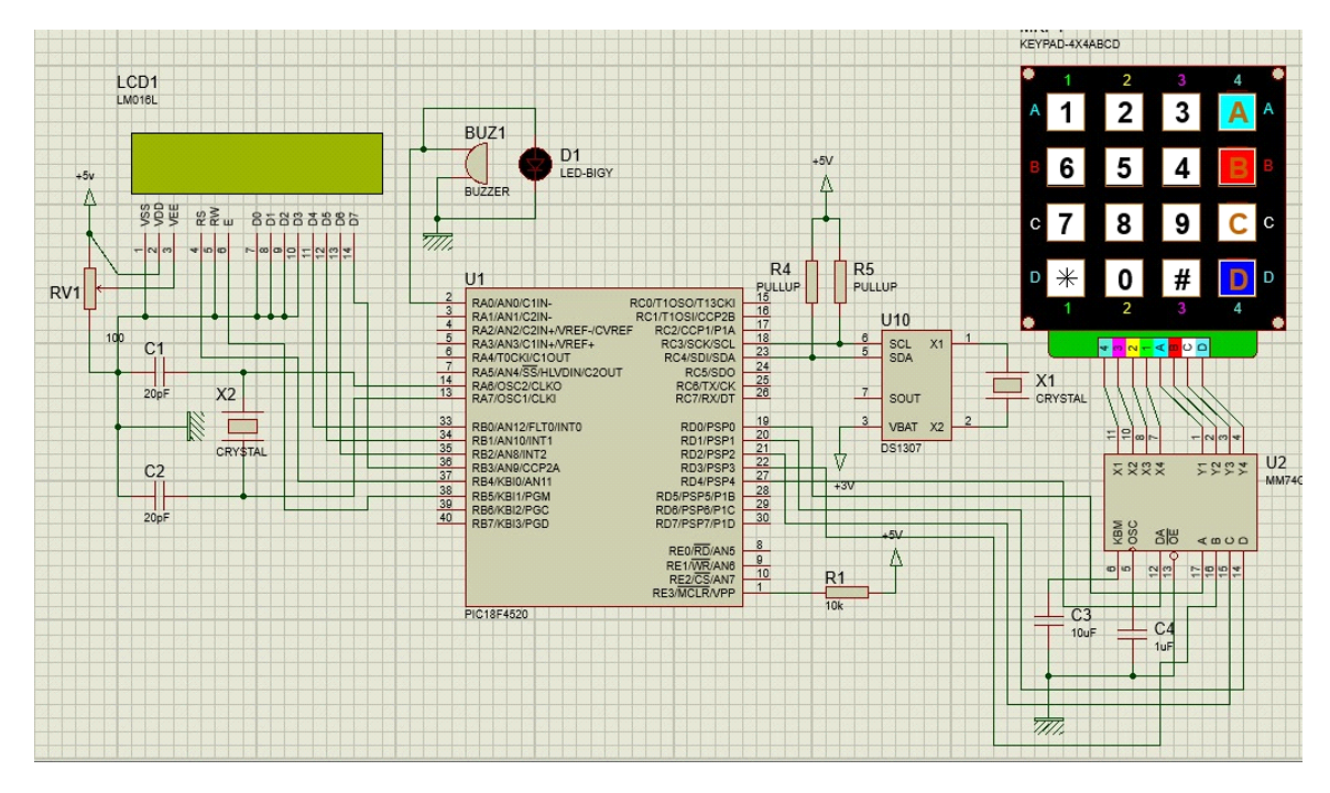
I used PIC18f4520 microcontroller as the brain of the system. RTC1307 IC is used to maintain the clock,date and day with a 3V backup voltage battery. Bell timings are stored in the internal EEPROM of mcu.

MCU is reading time from RTC through I2C Serial protocol and compares the current time with stored memory time in a continous while(1) loop.

MM74C922 decoder IC is used for keyboard. Reading the sixteen buttons is done using 4-bits output of decoder IC.

Photos

3D_PCB_th

photo_1_th

photo_3_th

photo_4_th

photo_5_th

photo_6_th

24×6 LED Matrix Control Circuit

image_1

LED_board

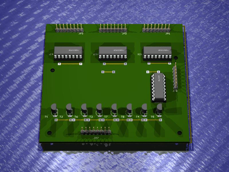
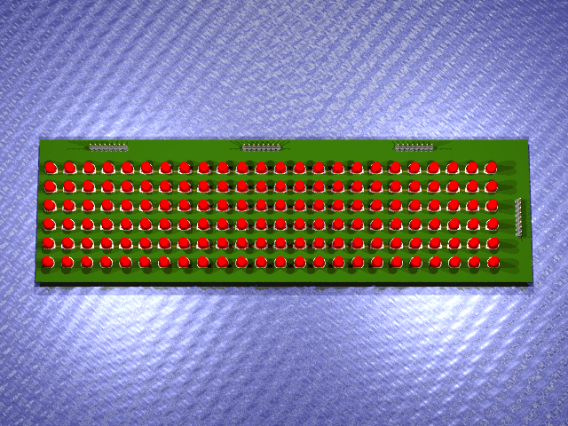
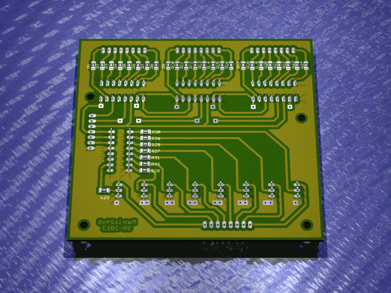
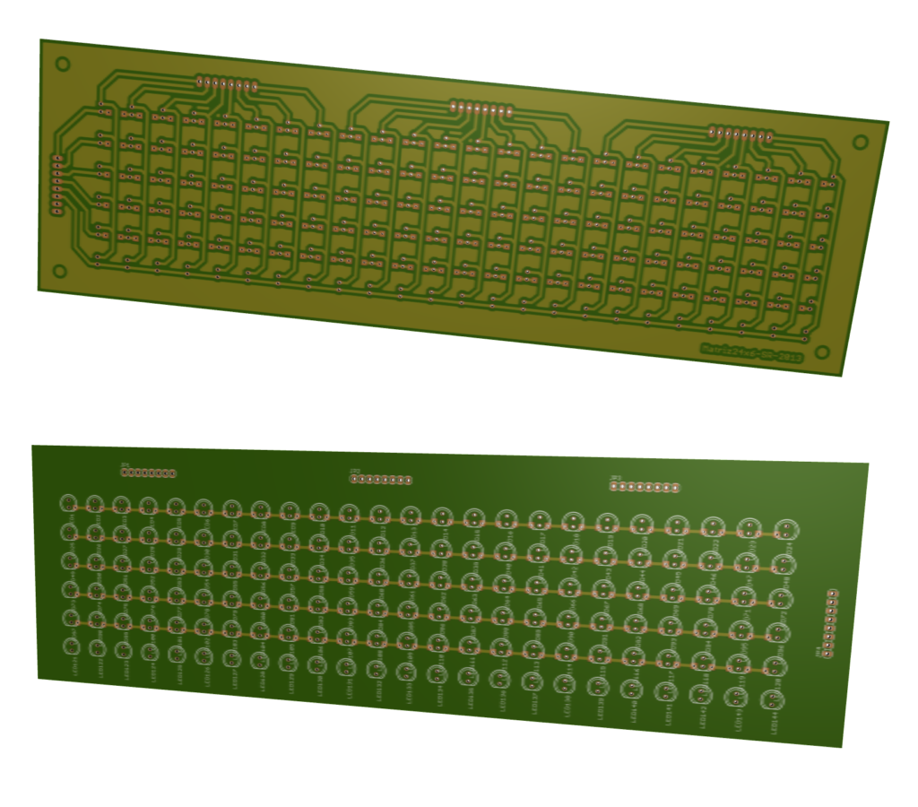
This is a 24×6 LED matrix control board based on Syst3mX schematics on Instructables. The board is connected on the LED matrix board and an external MCU or Arduino is required to produce the control signals that are feed on GP8.

Control Board Schematic

control_board_schematic_th

Description

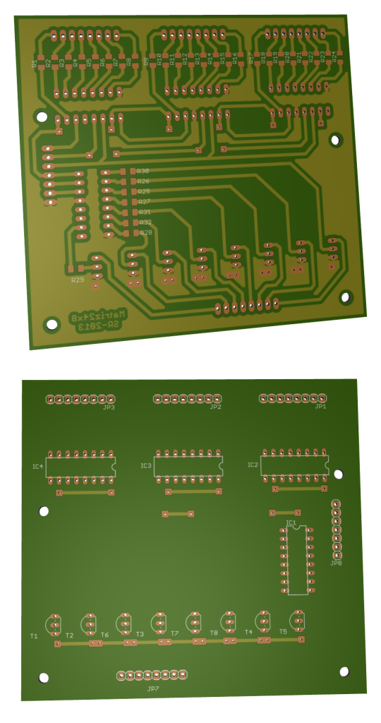
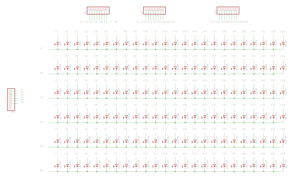
The circuit is able to drive a 24×6 LED matrix using an external MCU or Arduino board.  The LED matrix columns are connected on JP1, JP2, JP3 and the 6 rows are connected on JP7. There is also the option to connect 2 more rows (total 8 rows) to make a 24×8 LED matrix.

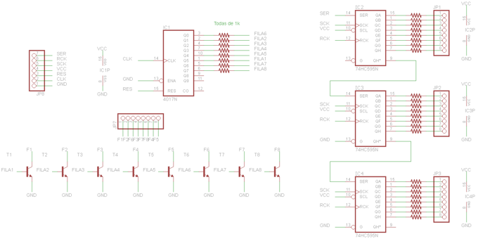
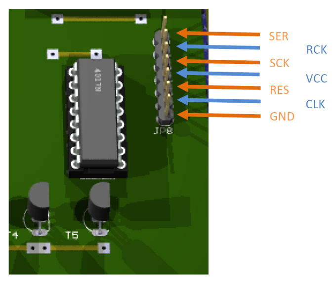
The control is done externally applying the signals on JP8 as is shown on the diagramm below:

image_3

  • GND is the signal ground
  • VCC is 5V in reference to GND
  • RCK is SC signal of SPI (latch)
  • SCK is CLOCK signal of SPI
  • SER is DATA dignal of SPI
  • CLK is CLOCK signal of 4017
  • RES is RESET signal of 4017

Control signals can be easily generated by an Arduino UNO or Duemilanove using some code . You may refer to:

Parts

R25, R26, R27, R28, R30, R31, R32 6 x Resistors of 1k Ohms. SMD, 1206
The rest of resistors in the design 24 x Resistors of about 100 Ohms. SMD, 1206
IC1 1 x 4017 (decade counter) DIP
T1, T2, T3, T4, T5, T6, T7, T8 8 x 2N3904
IC2, IC3, IC4 3 x 74HC595 (shift register) DIP
JP1, JP2, JP3, JP6, JP7 5 x Pin Header (8×1)
4 x 3 mm screws

Control Board PCB Design
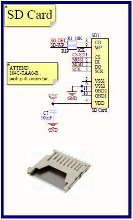
image_2

3D_Control_board_PCB

3D_LED_board_PCB

LED Board Schematic

LED_board_schematic

TOP PCB Companies