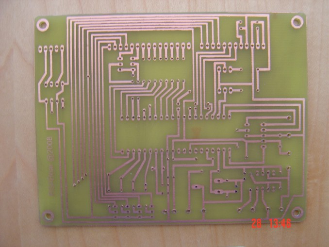
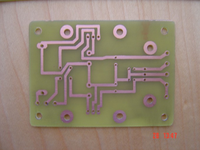
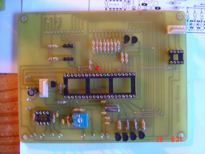
3-Wire Serial LCD using a Shift Register

Photo_4

Introduction

HD44780 based character LCDs require at least 6 I/O lines from microcontroller to display data. Therefore, they are not suitable for low-pin microcontrollers like PIC12F series microchips. In this project, I am going to show how to drive an HD44780 based LCD display with only 3 pins of a microcontroller. I am going to demonstrate it with PIC12F683 microchip. The character data and command from the microcontroller is transferred serially to a shift register (74HC595), and the parallel output from the shift register is fed to LCD pins.

About 74HC595

74HC595 is a high-speed 8-bit serial in, serial or parallel-out shift register with a storage register and 3-state outputs.

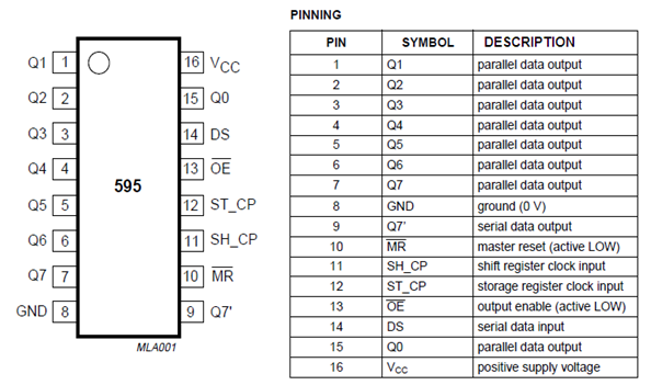
Pinout_1

The shift register and storage registers have separate clocks, SH_CP and ST_CP respectively. Data in the shift register is shifted on the positive-going transitions of SH_CP, and the content of shift register will be transferred to the storage register on a positive-going transition of the ST_CP. If we tie both the clocks together, the shift register will always be one clock ahead of the storage register. The 8-bit data of the storage register will appear at the parallel output (Q0-Q7) when the output enable (OE) is low.

In this project, SH_CP and ST_CP are tied together. So, if we want to receive a serially transferred 8-bit into parallel form at Q0-Q7, an extra clock pulse is required after transmitting the 8-th bit of serial data because the clocks are tied and the storage register is 1-clock behind the shift register.

HD44780-based character LCD

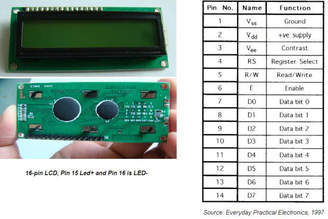
All HD44780 based character LCD displays are connected using 14 wires: 8 data lines (D0-D7), 3 control lines (RS, E, R/W), and three power lines (Vdd, Vss, Vee). Some LCDs may have LED backlight and so they may have additional connections (usually two: LED+ and LED-).

Pinout_2

Providing detail explanation of individual LCD pin doesn’t fall within the scope of this project. If you are a beginner with LCD, I recommend to read these two articles first from Everyday Practical Electronics magazine : How to use intelligent LCDs

Circuit Diagram

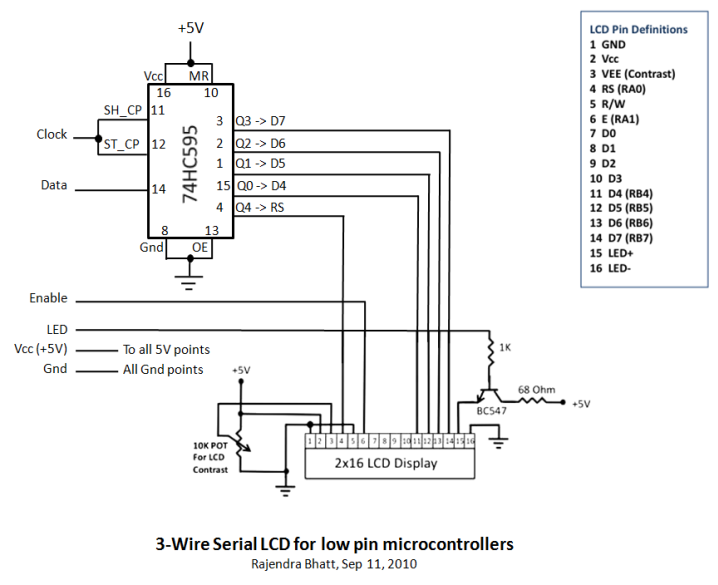
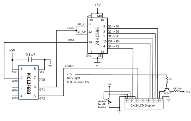
The hardware part of this project is fairly simple. The challenging part is to write the driver software that is responsible for a proper sequence of operations required to serially transfer character data and command to 74HC595 serial-in parallel-out shift register. The shift register parallel output is then connected to LCD data lines (D4-D7) and RS control pin. This arrangement requires 3-pins of microcontroller to display character data on a parallel LCD display: 2 pins for providing Clock and Data to 74HC595, and 1 pin for enable control (E) pin of LCD module. Since the data transfer uses 4-bit mode, any 8-bit command or character data is sent in two steps: send the higher nibble first, and then the lower nibble. The R/W control pin is grounded, and therefore no data or status read from the LCD module is possible in this case.

Schematic_1

The SH_CP (11) and ST_CP (12) clock inputs of 75HC595 are tied together, and will be driven by one microcontroller pin. Serial data from microcontroller is fed to the shift register through DS (14) pin. OE (13) pin is grounded and reset pin MR (10) is pulled high. Parallel outputs Q0-Q3 from 74HC595 are connected to D4-D7 pins of the LCD module. Similarly, Q4 output serves for RS control pin. If the LCD module comes with a built-in backlight LED, it can simply be turned ON or OFF through LED control pin shown above. Pulling the LED pin to logic high will turn the back light ON.

Photo_2

Photo_3

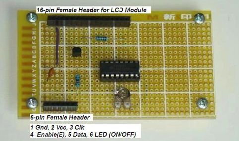
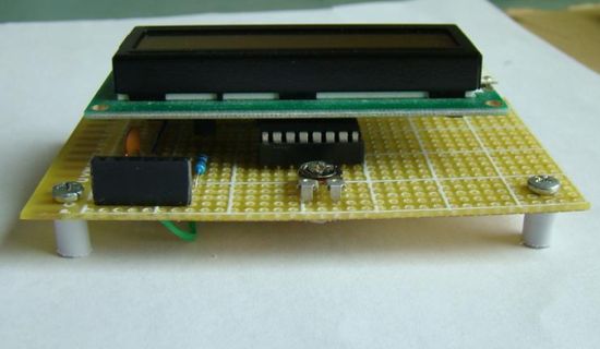
Circuit soldered on a general purpose prototyping board

Software

A first, a bit of data fed to DS pin of 74HC595 appears at Q0 output after 2 clocks (because SH_CP and ST_CP are tied). So, sending 4-bit data (D4-D7) and an RS signal require 6 clock pulses till they appear at Q0-Q4 outputs respectively. When the LCD module is turned ON, it is initialized in 8-bit mode. A number of initializing commands should be sent to operate the LCD module in 4-bit mode. All the driver routines that are discussed here are written in mikroC compiler. They work only for a 16×2 LCD module. User can modify the initialization operations inside the Initialize_LCD() routine to account for other LCD configurations. The driver routines and their functions are described below.

  • Initialize_LCD() : It initializes the LCD module to operate into 4-bit mode, 2 lines display, 5×7 size character, display ON, and no cursor.
  • Write_LCD_Data() : Sends a character byte to display at current cursor position.
  • Write_LCD_Cmd() : Write a command byte to the LCD module.
  • Write_LCD_Nibble() : Data or command byte is sent to the LCD module as two nibbles. So this function routine takes care for sending the nibble data to the LCD module.
  • Write_LCD_Text() : This routine is for sending a character string to display at current cursor position.
  • Position_LCD() : To change the current cursor position

At the beginning of your program, you need to define Data_Pin, Clk_Pin, and Enable_Pin to the chosen microcontroller ports. I am going to demonstrate here how to use these driver routines to display two blinking character strings, Message1 and Message2, at different locations. I am going to test our serial LCD module with PIC12F683 microcontroller. The test circuit is shown below.

Note: My PIC12F683 Settings

Running at 4 MHz internal clock, MCLR disabled, WDT OFF.

lock, Data, and Enable lines are served through GP1, GP5, and GP2 ports.

Schematic_2

Code

/* 3-wire Serial LCD using 74HC595
Rajendra Bhatt, Sep 6, 2010
*/
 
sbit Data_Pin at GP5_bit;
sbit Clk_Pin at GP1_bit;
sbit Enable_Pin at GP2_bit;
 
// Always mention this definition statement
unsigned short Low_Nibble, High_Nibble, p, q,  Mask, N,t, RS, Flag, temp;
 
void Delay_50ms(){
 Delay_ms(50);
}
 
void Write_LCD_Nibble(unsigned short N){
 Enable_Pin = 1;
 // ****** Write RS *********
 Clk_Pin = 0;
 Data_Pin = RS;
 Clk_Pin = 1;
 Clk_Pin = 0;
 // ****** End RS Write
 
 // Shift in 4 bits
 Mask = 8;
  for (t=0; t<4; t++){
   Flag = N & Mask;
   if(Flag==0) Data_Pin = 0;
   else Data_Pin = 1;
   Clk_Pin = 1;
   Clk_Pin = 0;
   Mask = Mask >> 1;
  }
  // One more clock because SC and ST clks are tied
  Clk_Pin = 1;
  Clk_Pin = 0;
  Data_Pin = 0;
  Enable_Pin = 0;
  Enable_Pin = 1;
}
// ******* Write Nibble Ends
 
 void Write_LCD_Data(unsigned short D){
 RS = 1; // It is Data, not command
 Low_Nibble = D & 15;
 High_Nibble = D/16;
 Write_LCD_Nibble(High_Nibble);
 Write_LCD_Nibble(Low_Nibble);
 }
 
void Write_LCD_Cmd(unsigned short C){
 RS = 0; // It is command, not data
 Low_Nibble = C & 15;
 High_Nibble = C/16;
 Write_LCD_Nibble(High_Nibble);
 Write_LCD_Nibble(Low_Nibble);
}
 
void Initialize_LCD(){
 Delay_50ms();
 Write_LCD_Cmd(0x20); // Wake-Up Sequence
 Delay_50ms();
 Write_LCD_Cmd(0x20);
 Delay_50ms();
 Write_LCD_Cmd(0x20);
 Delay_50ms();
 Write_LCD_Cmd(0x28); // 4-bits, 2 lines, 5x7 font
 Delay_50ms();
 Write_LCD_Cmd(0x0C); // Display ON, No cursors
 Delay_50ms();
 Write_LCD_Cmd(0x06); // Entry mode- Auto-increment, No Display shifting
 Delay_50ms();
 Write_LCD_Cmd(0x01);
 Delay_50ms();
}
 
void Position_LCD(unsigned short x, unsigned short y){
 temp = 127 + y;
 if (x == 2) temp = temp + 64;
 Write_LCD_Cmd(temp);
}
 
void Write_LCD_Text(char *StrData){
 q = strlen(StrData);
 for (p = 0; p<q; p++){<br="">  temp = StrData[p];
  Write_LCD_Data(temp);
 }
 
}
 
char Message1[] = "3-Wire LCD";
char Message2[] = "using 74HC595";
 
void main() {
CMCON0 = 7;  // Disable Comparators
TRISIO = 0b00001000;  // All Outputs except GP3
ANSEL = 0x00; // No analog i/p
 
Initialize_LCD();
 
do {
 Position_LCD(1,4);
 Write_LCD_Text(Message1);
 Position_LCD(2,2);
 Write_LCD_Text(Message2);
 Delay_ms(1500);
 Write_LCD_Cmd(0x01);  // Clear LCD
 delay_ms(1000);
} while(1);

}


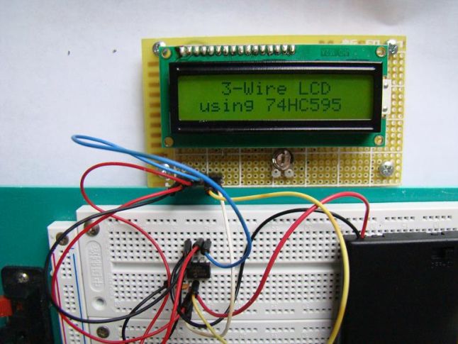
Test Circuit and Output

Photo_4
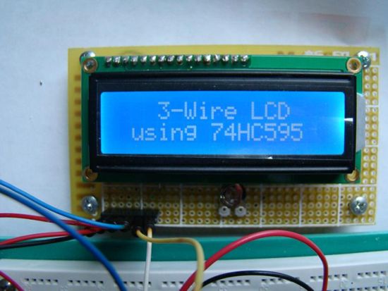
Photo_5_th

Testing with a different LCD module
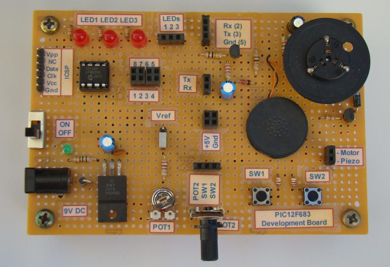
Learning Board for Microchip PIC12F683 microcontroller

photo_3

Introduction

Electronics is my hobby. When I was in college I had some experience with microcontrollers; I did few projects with Atmel’s AT89C51. Recently, I have grown interest on PIC microcontrollers, and I thought I should start with 8-pin microchips. I picked PIC12F683 microchip. This microcontroller fascinated me a lot because I wanted to see what we can do with an 8-pin microcontroller (out of which 2 pins goes to power supply, so actually just 6-pins are left for I/O). So I thought of making my own learning board for this. In this project, I am first going to describe the learning board that I made, and then will demonstrate few experiments on it.

Some of the features of PIC12F683:

  • Wide operating voltage range (2.0-5.5V)
  • Precision internal oscillator (software selectable, 8 MHz to 125 Khz)
  • 6 I/O pins with interrupt-on-change features.
  • Four 10-bit A/D converters
  • Two 8-bit and one 16-bit timers
  • One Capture, Compare, PWM module
  • In-Circuit Serial Programming
  • Program Memory- 2048 words, SRAM- 128 bytes, EEPROM-256 bytes

Circuit Layout and Design

This learning board has the following features:

  • A 9V DC input socket with power on switch
  • Regulated +5V power supply using 7805 IC
  • 3 output LEDs and 1 power on LED
  • 2 input tact switches
  • 2 potentiometers: one for analog input and the other for providing reference voltage for ADC
  • Transistor-based TTL-RS232 level converter for serial communication.
  • A DC motor with a transistor driver.
  • A piezo-buzzer

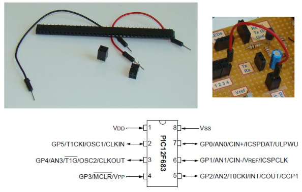
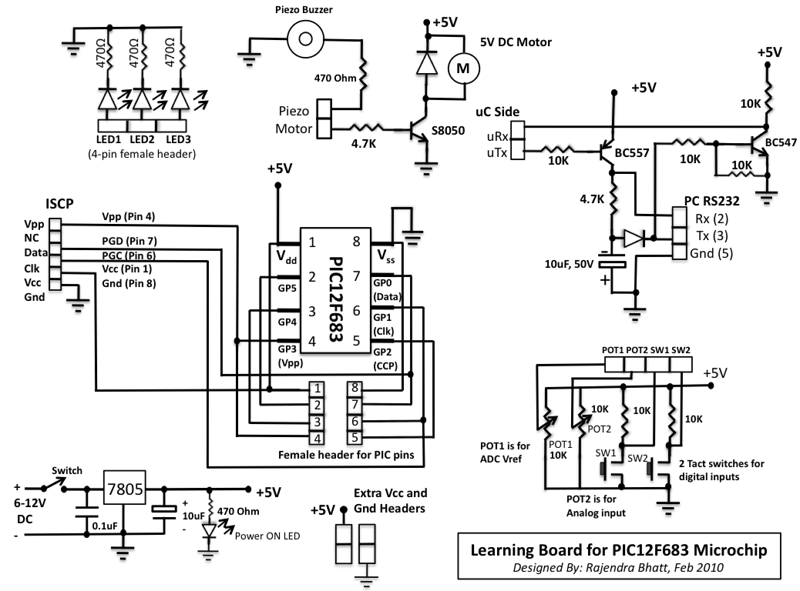
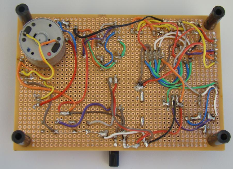
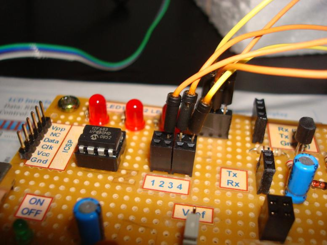
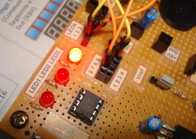
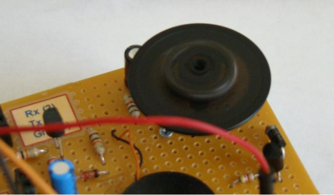
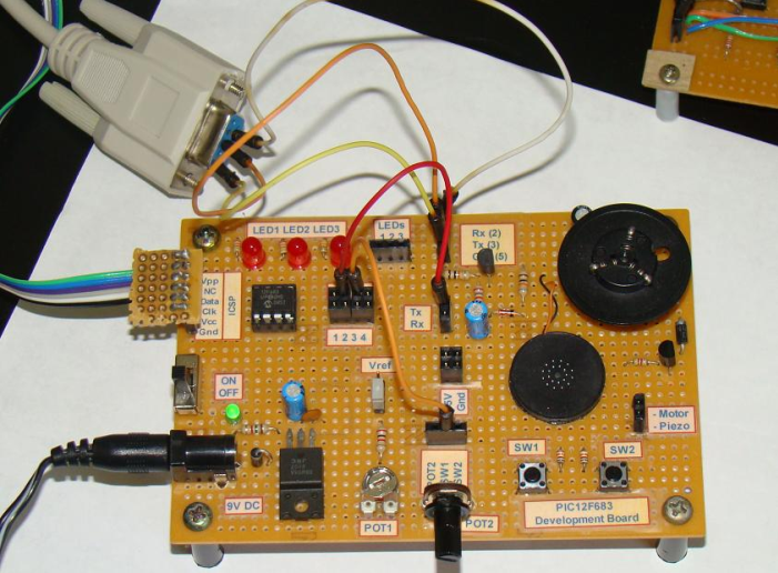
Most of these features on the board are accessible through female header pins. None of the 6-I/O pins of PIC12F683 are hardwired to anything and they are accessible through header pins too. The figures  below show PIC12F683 pins, the type of female headers and jumpers used to make connection on the board, and the detail circuit diagram of the learning board. Only the ISCP pins are accessible through male header pins. The entire circuit is built on a 8 x 12 cm general prototyping board.

photo_1

photo_2

As you see the output LEDs have 470Ω current limiting resistors in series so that a PIC pin can be safely drive them. The piezo buzzer is also driven directly by a PIC pin through a series resistor. The DC motor, however, is connected as a load to the collector of S8050 transistor as the required current to drive the motor cannot be supplied by the PIC port. So, the PIC port can switch on the transistor by pulling its base HIGH and the collector current of the transistor provides the sufficient current to drive the motor.

The TTL to RS232 level converter and vice-versa is achieved with two transistors and few other components. The negative voltage required for RS232 level is stolen from the RS232 port of a PC itself. Note that there is no hardware UART inside PIC12F683, so the serial data transfer from the microcontroller to PC will be possible only through a software UART through any of GP0, GP1, GP2, GP4, and GP5 ports (GP3 is input only). The transmitter and receiver port on microcontroller side are denoted by uTx and uRx, whereas on the PC side are denoted by Tx and Rx, respectively.

The circuit diagram shows that the two input tact switches with the two potentiometer outputs and all the eight PIC12F683 pins are accessible through female headers. The tact switches are active low, i.e., under normal condition, a tact switch output is HIGH and when it is pressed, the output is LOW. There are couple of extra headers for Vcc and Gnd terminals which may be required while doing experiments.

he power supply circuit is the standard circuit of 7805 regulator IC. A power-on LED is connected across Vcc and Gnd with a 470Ω series resistor.

The in-circuit serial programming (ICSP) of PIC12F683 can be done with two pins: ICSPDAT (pin 7), and ICSPCLK (pin 6). The programming voltage, Vpp, should be provided to pin 4 of PIC12F683 while programming. All the required ISCP pins are available through a male header, so the PIC can be programmed through any ICSP PIC programmer. Make sure that the sequence of ISCP pins on the programmer side and our learning board match.

During ICSP, pins 4, 6, and 7 of PIC12F683 should not be connected to anything; leave them open so that there won’t be any voltage conflict between the programmer and the external circuit.

Software Development

You can write your experimental programs for PIC12F683 in assembly or high level language. But for the experiments that I am going to demonstrate here, I am using the free version of mikroC compiler from MikroElektronica. It is a C compiler for PIC microchips, and the free version limits output program size to 2K. But we don’t need more than that for PIC12F683.

We will use the following configuration bits for PIC12F683. In mikroC, you can select these in Edit Project window.

Oscillator : Internal RC, No Clock
WDT OFF
Master Clear Disabled

For all the experiments demonstrated here, use internal clock at 4.0 MHz.

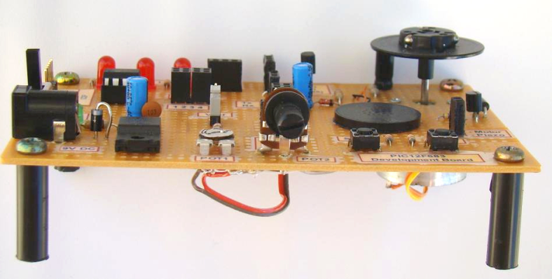
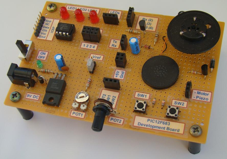
Completed Learning Board for PIC12F683

photo_4

photo_5

photo_6

Test Experiments

Read once again the Software Development section above before proceeding.

Experiment No. 1: 3-bit Binary UP Counter

The objective of this experiment is to build a 3-bit binary Up-counter that counts from 000 to 111 with 1 sec delay between each count. After it gets to 111, it resets to 000 and starts counting again. The count value will be displayed on three LEDs.

Setup: Connect GP0, GP1, and GP2 (PIC pins 7, 6, and 5) to LED 3, 2, and 1 respectively.

photo_7

/*
  PIC12F683 Experiment Board
  Experimen No. 1 : 3-bit Up Counter
  "LEDs 1, 2, and 3 are connected to GPIO2, GPIO1, and GPIO0
   respectively"
*/

short i;
void main() {
CMCON0 = 7; // Disable comparators
TRISIO = 8;  // GPIO0-GPIO2 are Outputs, GP3 is default input
ANSEL = 0;  // No ADC
GPIO = 0;
delay_ms(500);
i=0;
do {
   GPIO=i;
   delay_ms(1000);
   i = i+1;
   if(i == 8) i=0;

   }while(1);
}

Compile this program in mikroC and load it inside PIC12F683 with any ICSP programmer.

Output:

photo_8

3-bit counter shown on LEDs

Experiment No. 2: Tact switch inputs and Motor control.

The objective of this experiment is to control a motor with two tactile switches. When one switch is pressed, the motor will turn ON, and the other will make it OFF.

Setup: Connect the SW1 and SW2 pins to GP0 (pin 7) and GP1 (pin 6) of PIC12F683. Also connect the motor drive pin to GP2 (pin 5). So, GP0 and GP1 are inputs and GP2 is output. Remember that when a switch is pressed, the corresponding SW pin is pulled LOW. Under normal conditions, SW1 and SW2 are pulled HIGH.

Software

/* Motor ON/OFF control with tact switches
 Rajendra Bhatt, Sep 3, 2010
 PIC12F683, MCLR OFF, Internal Oscillator @ 4.00MHz
 */

sbit Start_Button at GP0_bit;
sbit Stop_Button at GP1_bit;
sbit Motor at GP2_bit;

void main() {
CMCON0 = 7;  // Disable Comparators
TRISIO = 0x03;  // 0000 0011 GPIO 0, 1, Inputs; Rest are O/Ps
ANSEL = 0x00;
Motor = 0;

 do {
  if (!Start_Button) {     /* When a tact switch is pressed, Logic I/P is 0*/
  Delay_ms(100);
  Motor = 1; // Turn Motor ON
  }
  if (!Stop_Button) {
 Delay_ms(100);
 Motor = 0; // Turn Motor ON
  }
 } while(1);
}

Output: When SW1 is pressed ON, the motor will turn ON, and when SW2 is pressed it will turn OFF.

photo_10

Experiment No. 3: Software UART test.

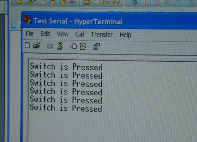
The objective of this experiment is to send a character string to PC using a software UART routine. The string will be transferred to PC and displayed on a Hyperterminal window when SW1 switch is pressed. The character string will be “Switch is Pressed”

Setup:Microcontroller side: Connect the uTx and SW1 pins to GP0 (pin 7) and GP1 ports respectively.

PC Side: Connect Rx (2), Tx (3), and Gnd (5) pins on the board to the corresponding RS232 port pins of the PC. Also, define a new connection hyperterminal window on a PC with the following settings.

BPS = 9600; Data bits = 8; Parity = None; Stop bits = 1; Flow Control = Hardware

photo_11

Software

/*
  UART Test Experiment
  Rajendra Bhatt, Sep 4, 2010
  SW1 at GPIO1, uTx at GPIO0
*/
char Message[] = "Switch is Pressed";
char error;
int i;
void main() {
CMCON0 = 7;
TRISIO = 0x02;  // 0000 0010. GPIO 1 input; Rest are O/Ps
ANSEL = 0;
// Define GPIO.3 as UART Rx, and 0 as Tx
error = Soft_UART_Init(&GPIO,3, 0, 9600, 0 );
 do{
  // Detect logical one to zero
  if (Button(&GPIO, 1, 1, 0)) {
     Delay_ms(300);
     for (i=0; i< 17; i++) {
      Soft_UART_Write(Message[i]);
      Delay_ms(50);
     }
     Soft_UART_Write(10); // Line Feed
     Soft_UART_Write(13); // Carriage Return
  }
 
 
 }while(1);
 
}

Output: Everytime SW1 id pressed, you will see the character string “Switch is Pressed ” displayed on the hyperterminal window.

photo_12

Experiment No. 4: Analog-to-digital conversion and software UART.

The objective of this experiment is read an analog voltage from a potentiometer, convert it to 10-bit digital number, and serially transfer it to a PC. The digital number will be displayed on a hyper terminal window.

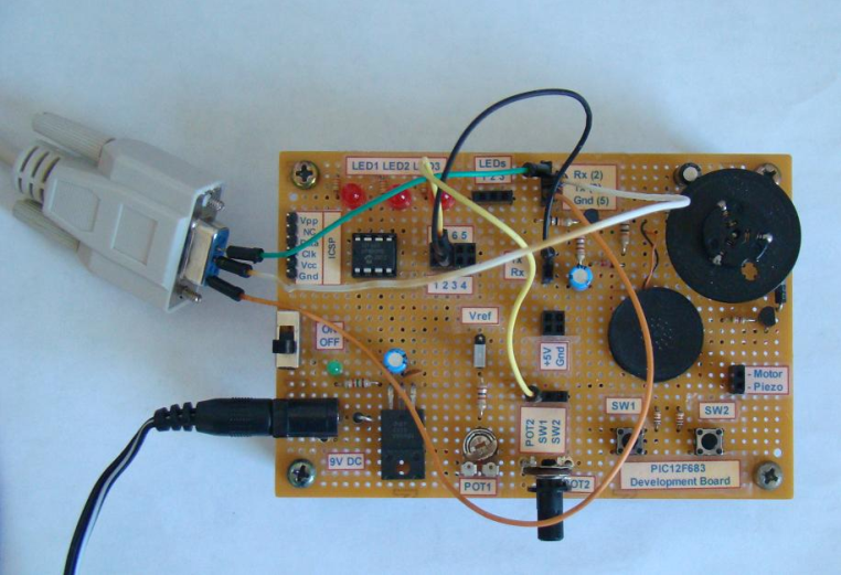
Setup: Connect the output of potentiometer (POT2) to AN0 (pin 7). GP5 (pin 2) will serve as TX pin for Software UART so connect it touTx pin of TTL to RS232 Level Shifter circuit. Also connect Tx(3), Rx (2) and Gnd (5) pins on the board to corresponding pins of RS232 port of the PC.

photo_13

Software

/*

  PIC12F683 Experiment Board
  Experimen No. 3 : Read analog voltage from AN0 and diplay
  on Hyperterminal window on PC using Software UART.
  Date: 06/25/2010
*/
char Message1[] = "Digital Value= ";
unsigned int adc_value, backup=0 ;
char *temp = "0000", error;
int i;
void main() {
CMCON0 = 7;
TRISIO = 11;  // GPIO 0, 1, 3 Inputs; Rest are O/Ps
ANSEL = 0;
GPIO = 0;
// Define GPIO.3 as UART Rx, and 5 as Tx
error = Soft_UART_Init(&GPIO,3, 5, 9600, 0 );
Delay_ms(100);
 
do {
 adc_value = ADC_Read(0);
 
 
 if(adc_value != backup) {
 
  if (adc_value/1000)
   temp[0] = adc_value/1000 + 48;
  else
  temp[0] = '0';
 
  temp[1] = (adc_value/100)%10 + 48;
  temp[2] = (adc_value/10)%10 + 48;
  temp[3] = adc_value%10 + 48;
 
 for (i=0; i<= 13; i++) {
      Soft_UART_Write(Message1[i]);
      Delay_ms(50);
     }
 
 for (i=0; i<= 3; i++) {
      Soft_UART_Write(temp[i]);
      Delay_ms(50);
     }
     Soft_UART_Write(10); // Line Feed
     Soft_UART_Write(13); // Carriage Return
 
 backup = adc_value;
 }
 
 delay_ms(100);
 } while(1);
}

Output

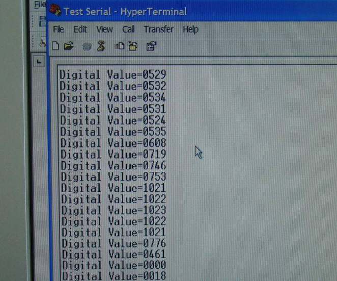
A digital number corresponding to the analog input will be displayed on the hyperterminal window. You can vary the potentiometer and the digital equivalent number will also change. Remember, the ADC is 10-bit so the number you see on the screen will be from 0000 to 1023.

photo_14

More experiments will be posted on http://picboard.blogspot.com in future.

Build your Own PCB Exposure Box with Fluorescent Lamps and Countdown System

photo_1

Introduction

Tired of spending hours and hours in wire soldering? Do your circuits look ugly and you are looking for a way to produce professional-like PCBs? Then you had better try photoetching. And the first step to do that is to have the right equipment that is an Automated Exposure Box. Moreover if you like tinkering with microcontrollers, here is the challenge and it’s high time you launched the design of your own PCB Exposure Box.

photo_2

ss


In the following lines I describe the procedure I followed to build the Box, the Lamp System and the Countdown System which is based on the AVR mega8 microcontroller.

Brief Description

Four blacklight lamps, 15W each, emit radiation at the region of UVA, with a peak around 350nm where the thin surface above the copper of the photosensitive board, is… sensitive. The lamps are taken by two and are connected in series thus shaping two similar modules. Each module has its own ballast and can be connected to 220V AC via a relay.
A microcontroller counts a user defined countdown and upon reaching zero activates a relay. The time remaining is displayed on four 7-segment led displays. The maximum countdown is 99 minutes and 59 secs.

The desired countdown is entered using only two buttons, SET and START/STOP. Short term push of the SET button will increase the current digit while prolonged push will change the digit from secondss to decades of seconds, to minutes and so on. Pushing once the START/STOP button, will make the MCU accept the desired countdown. Pushing the START/STOP button one more time, will start the countdown and connect the lamp system to 220V AC, via the relay. If START/STOP button is pushed again before countdown reaches zero, the lamp system will be deactivated. When the countdown reaches zero the lamp system is deactivated and a 3 seconds beep is sounded. The timer remembers the last used countdown and uses it as default every time the system is switched on.

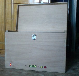
All things above are housed in a wooden box. You can design the box by yourself however I had it done by a technician.

There are 3 distinctive parts that constitute your PCB Exposure Box; the Box the Lamp System and the Counter System along with the display.

The Box

photo_3

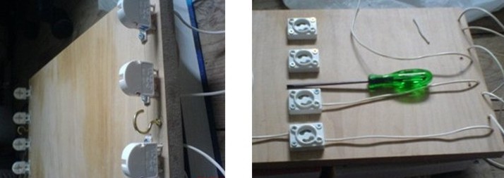
You are gonna need a wooden box with dimensions aproximately 50x30x60 cm3. The box must have an extra room for hosting the countdown board and the two ballasts. The height of that room, that is the distance between the bottom of the box and the shelf, can be 5-8 cm. On the one side of the shelf will be installed the four starter bases and on the other side the four lamps along with their G13 bases.

Here is a very detailed description on how to build your own box, upon which I relied to decide the dimensions of my box. However the final design I used is the same as Papanikolaou’s box in his Darkroom Timer project. Many thanks to both of them!

The Lamp System

For the lamp system you will need:

  • 4 x 15W Black Light UVA fluorescent lamps with a peak of radiation at ~350nm. Those lamps are suitable for photochemical procedures and can usually be used in insect killing. Examples are F15W/T8/BL from Syllvania and Actinic BL from Phillips
    (approx. cost 10€/lamp)
  • 2 x 40W Ballast. This is the common ballasts used in fluorescent lamps (approx. cost 2€/ballast)
  • 4 x Starters that can support 15W lamps
    (ex 22W starters approx. cost 0.5€/starter)
  • 4 x Starter bases
    (approx. cost < 0.2€/base)
  • 8 x Bases for the lamps with holes so they can be screwed on the wood (approx. cost 0.6€/base)
  • Wire. Prefer flexible wire which is commonly used in fluorescent lamps.
  • 20 x Screws. Use the size you thing that best fits.

photo_4

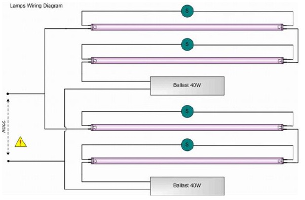
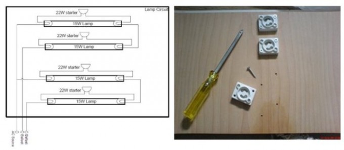
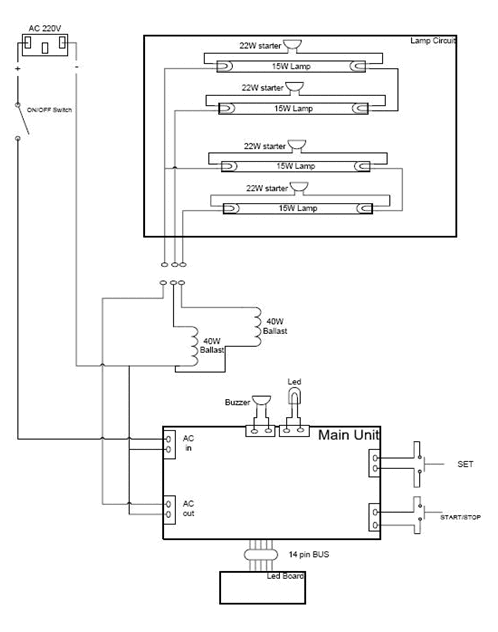
The connections you have to make for the lamps are as in the next image.

This is a very popular connection for two low wattage fluorescent lamps connected in series.

There are two identical modules connected in parallel. In each module, initially, the AC current flows through the two starters and the ballast. After a while, one of the starters goes open-circuited and the current in the circuit is halted. This brings the ballast inductor in an extremely uncomfortable situation and it reacts violently developing a great voltage across its terminals. The value of the voltage can be as large as some kV and that is exactly what the fluorescent lamps need in order to be turned on. After that transition effect, the voltage across each lamp gets stabilized around the 50~60V which is the lamp’s operation voltage shown in the manuals.

As for the construction details, I put the lamps and the starters on the two sides of the wooden shelf and the two ballasts on the bottom of the box.

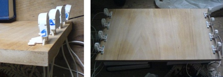
So, as far as the shelf is concerned. First, I screwed the starters’ bases on the I made the following connections one side of the shelf

photo_5

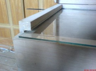
Second, on the other side of the shelf, I screwed the eight G13 lamp holders, having first, drilled the holes needed by the wires to join the lamp bases with the starter bases

photo_6

also don’t forget to screw some shelve holders so that you can put and get out the shelf from the box, next do the wire connections

photo_8

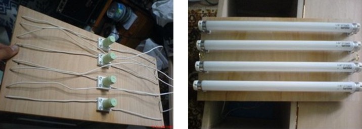
and finish the shelf by populating it with the starters and the lamps

photo_7

The finished lamp system looks like

photo_9

The Countdown Timer

This is the most amusing part of the story. Here you have to deal with Software and Hardware.

>As for the Software part I wrote the code in C using the winAVR and avr-gcc plugin along with avrStudio. Using ProteusVSM I tested the code in a simulation environment which saved me a lot of effort and time. Then I downloaded the hex code to the chip with the STK500. I strongly recommend that you try and write the code by yourself so I don’t attach any code here except for the downloadable hex. If you need any help about the code, please mail me at aetheod @ hotmail.com

As for the hardware, there has been a lot talk about how to do it. The Darkroom Timer of Vassilis Papanikolaou contains quite apprehensive schematics plus PCBs. My schematic contains all the variations required for the substitution of the PIC with the AVR mega8. In addition I use only two buttons and I put the regulators in parallel instead of in series.

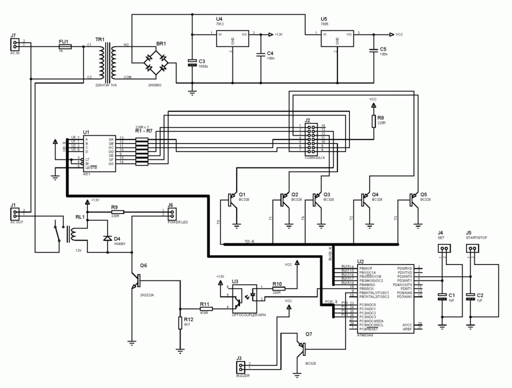
The schematic of the main unit which contains the microcontroller and the power supply is the following:

main_schematic

Parts

QTY PART-REFS VALUE
— ——— —–

Resistors
———
10 R1 – R10 220R
1 R11 470R
1 R12 4K7

Capacitors
———-
2 C1,C2 1uF
1 C3 1000u
2 C4,C5 100n

Integrated Circuits
——————-
1 U1 CD4511 BCD to 7segm. Com. Cath. Decoder
1 U2 ATMEGA8 AVR 8bit RISC microcontroller
1 U3 OPTOCOUPLER-NPN
1 U4 7812 12V Regulator
1 U5 7805 5V Regulator

Transistors
———–
6 Q1-Q5,Q7 BC328 pnp 800mA transistor
1 Q6 2N2222A npn 800mA transistor

Diodes
——
1 D4 1N4001

Miscellaneous
————-
1 BR1 Any diode bridge > 1A
1 FU1 1A fuse
1 J1 AC OUT socket
1 J2 CONN-DIL14 14 pin header for the connection with the
led board
1 J3 BUZZER
1 J4 SET button
1 J5 START/STOP button
1 J6 POWER LED
1 J7 AC IN socket
1 RL1 12V relay
1 TR1 220V/14V 1VA transformer (from an old Radio)

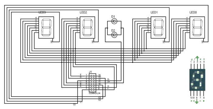
LED BOARD SCHEMATIC

led_display_schematic_th

QTY PART-REFS VALUE
— ——— —–
Diodes
——
2 D1,D2 LED-GREEN

Miscellaneous
————-
1 J1 CONN-DIL14 for the connection with the main unit
4 LED0-LED3 Common Cathode 7segment displays

I tested the schematic virtually and in real-time. And by “virtually” I mean I used an Electronics Systems Simulation Software like Proteus VSM… and like nothing else (…coz as far as I know there is no competitor so far!). I am not doing any advertisement but Proteus VSM is amazing and for those who haven’t heard about it yet, I recommend that they try, at least, a demo version from www.labcenter.co.uk

Only after Proteus said I was right, did I try the circuit in a breadboard and that fact saved me a lot of time, especially in the code development and debugging. So saying “I tested the circuit in real time” I mean I put every component on the breadboard and there I fixed any problems that Proteus didn’t find.

In breadboard.flv video, there is a demonstration of the Countdown Timer working while being tested on the breadboard

So, after ensuring everything was right it was time to design my last wire-soldered circuit!

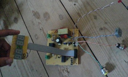
I started from the led board

photo_10

and the corresponding main unit

photo_11

Connecting the modules together

photo_12

desk_lights_off.flv is a video showing the Countdown Module in action turning off the light of my desk after 10 secs
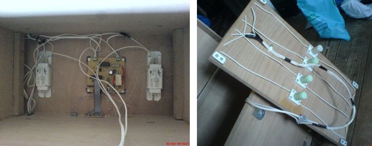
Putting all together…

So far so good! Everything works fine and it is time to enclose the Lamp System and the Countdown System in the Box. A general diagram helps to identify the place of each module.

overal_schematic

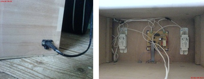
first a socket at the back of the box is installed, next the ballasts, the main board, the led board and the switches

photo_13

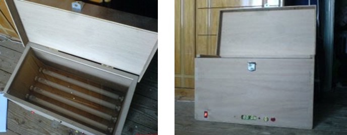
PCB Exposure Box is ready, and after the shelf is set

photo_14

in demo.flv video you can see the PCB Exposure Box working.

photo_15

As you noticed I put the camera recording and runaway(!), since UVA radiation is harmful and hazardous. Never do you look straight on the lamps.

That’s it

Well this is all about it! I hope this guide will give you the motivation to build your own PCB Exposure Box or at least to make you play with those little gems; the microcontrollers. To tell the truth I was motivated by similar guides and I am realy grateful to those who published them, sharing their experience with me and with the rest of “electromaniacs” around the world.

For any help, questions misunderstandings please mail me at aetheod @ hotmail.com

Special thanks to Vassilis Papanikolaou, Peter Makris and all the people of www.electronics-lab.com

The next step…

So if you succeeded upon building your own PCB Exposure Box you are ready now to make use of your device and print your first photoetched PCB. Here, is an excellent guide about photoetching from Peter Makris. Take a look…

PIC based WWVB clock

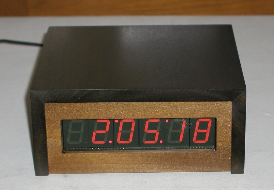
photo_1

Introduction

There are many DIY versions of WWVB clock designs available on the web. Commercial “atomic” clocks are inexpensive and widely available, but I wanted to try my hand at designing one to gain insight into WWVB reception and to learn a little about programming a PIC microcontroller. My version is not the simplest available, but it works well and I think it offers a few unique features.

WWVB Clock Features

  • Receives time broadcast from WWVB, Fort Collins, CO
  • Auto synchronizes internal time with WWVB time
  • Maintains local time when WWVB signal is lost
  • This version is for Pacific Standard Time, and auto detects/corrects for Daylignt Savings Time
  • 6-digit display of hours, minutes, seconds using 1″ seven-segment LED displays
  • WWVB sync indicator
  • Time display is in 12-hour format
  • PIC 16F628 microcontroller
  • Software written in C
  • All tools (schematic editor, C compiler, PCB layout software, PIC programmer are free and available for download on the web.

A complete description and specification for the WWVB broadcasts is available (free), document # 432, attf.nist.gov/general/pdf/1383.pdf The WWVB signal is broadcast as a 60 kHz carrier that is AM modulated with a time code frame that is updated once per minute. The data rate is one bit per second. Along with time code information, the data frame also contains synchronization bits, calendar data, UT1 correction, leap year, and leap second data. The clock design presented here only decodes the time data and daylight savings correction data. The software could easily be modified to include decoding of the other information bits, if desired. The the low frequency WWVB signal strength is weak and reception can be problematic. Signal acquisition time is variable, depending on location and atmospheric conditions. Reception is usually best at night between 8pm – 4am. To use the clock, just apply power and wait for reception of the WWVB signal. When the clock receives a complete error-free frame of data, it will automatically reset the display to show the correct time. After the initial time correction, the clock will maintain time even if WWVB reception is lost.

Hardware Description

schematic

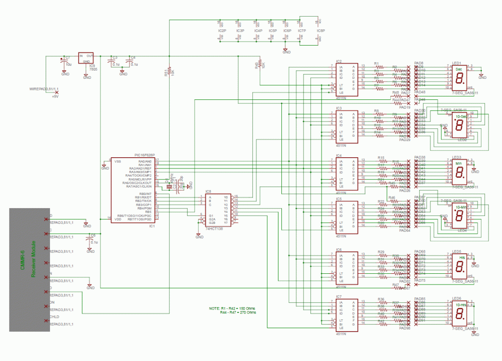
As shown in the schematic (pdf format), the heart of the clock is a PIC 16F628 microcontroller running at 4 MHz. Decoded time data is sequentially output from the microcontroller (RA0 – RA3) to the 7-segment decoder/drivers on a 4-bit data bus. The data is output sequentially as seconds, 10s of seconds, minutes, 10s of minutes, hours, and 10s of hours. The microcontroller outputs (RB1, RB2, RB3) route a 10 uSec stroble pulse from RB4 out to each of the 7-segment decoder/drivers at the proper time to latch the data bus values. Seconds and 10s of seconds display values are updated once per second. Minutes, 10s of minutes, hours, and 10s of hours are updated once per minute. The display consists of 1″ red-orange LED 7-segment displays. The decimal points on the displays are used to form colons to separate the seconds, minutes, and hours. The 10s of seconds and 10s of minutes displays are mounted upside down to form the upper colon dots. The WWVB receiver is a C-MAX model CMMR-6 and is available from Digi-Key (www.digikey.com) as part # 561-1014-ND complete with loopstick antenna. Data output from the receiver is sampled by the microcontroller on RB0.

Construction

photo_2_th

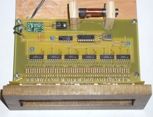
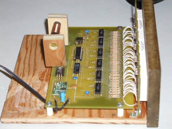
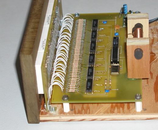
I have built two of these clocks, one using point-to-point wiring and one using a pcb. Both versions perform well. Just keep the receiver away from noise sources and the wire / trace lengths short to minimize inductance. I found that the receiver is also sensitive to magnetic fields produced by power supplies. I used a 9V, 200 mA “wall-wart” instead of an internal power supply to eliminate this problem.

My pcb was designed using Free PCB software www.freepcb.com. The artwork contains both the main board and the display board on a single layout to save the cost of two separate boards. I purchased the pcb from www.4pcb.com by sending them the gerber files and using their “bare-bones” process. The “bare-bones” process does not include solder mask nor silk-screen. Just cut off the display board from the main board and mount it at a right angle to the main board and wire them together using the pads provided.

photo_3_th

photo_4

Software description

I used the Source Boost C compiler to develop the software. It is available for free at www.sourceboost.com

The software is interrupt driven, from the PIC Timer 2 module. The basic timing is set to provide 32 interrupts/sec for both receiver sampling and for internal time propagation. The received data is sampled at 32 samples per second. The software cross correlates the input samples with stored “ideal” samples of the one, zero, and synch patterns. The beginning of a data frame is identified by two consecutive sync bits in a row. When this pattern is detected, the seconds data is reset to zero, and subsequent bits are detected as one’s or zero’s to extract the minutes and hours data. Only the data that is relevant to the time display is decoded. Bits within the data frame that do not contain time data are ignored. The bit detection cross-correlation algorithm requires 31 out of 32 sample agreements between the received data and the stored “ideal” sync pattern.

The decimal point on the seconds digit is turned on when sync is detected and turned off when sync is lost. Bit detection for one’s and zero’s require 28 out of 32 sample agreements between the received data and the stored “ideal” patterns. If any of the detected bits do not meet or exceed the correlation thresholds, the entire frame is discarded and a new search for frame sync is initiated. When sync and all of the time data within a frame is successfully detected, the data is corrected for Pacific Standard Time and Daylight Savings Time. The software must be changed for the proper corrections for other time zones. The time is also corrected for a one minute offset caused by WWVB time being valid at the start of each data frame. The fully corrected time is converted to a 12-hour format and then updates the internal time values. If the WWVB signal is lost, the internal time continues from where it was and relies on the PIC crystal oscillator to propagate time until the next WWVB data frame is received and validated. The PIC16F628 was programmed using WIN PIC software, available for free at

http://www.softpedia.com/get/Programming/Other-Programming-Files/PICProgrammer.shtml

and a “classic” style PIC burner to program the PIC – see

http://www.bobblick.com/techref/projects/picprog/picprog.html

Parts List

In the parts list, I have included the manufacturer and Digi-Key stock number for the ICs and parts that might be difficult to find. The resistors and capacitors are common parts that can be purchased from numerous vendors.

Component

Part Number

Description

Manufacturer

Digi-Key Stock #

IC1

PIC 16F628

Microcontroller

Microsemi

PIC16F628-04/P-ND

IC2 – IC7

4511N

BCD to 7-Segment decoder/driver

Various

296-3528-1-ND

IC8 74HCT138 3-8 decoder Various

296-1608-5-ND

IC9 7805 5V regulator Various LM7805CT-ND
R1 – R42 150 Ohm 1/8 W Resistor Various
R43, R51 10 k Ohm 1/8 W Resistor Various
R44 – 48 270 Ohm 1/8 W Resistor Various
Q1 4 MHz Crystal Various X971-ND
C1, C2 20 pf, 50V Capacitor Various
C3, C4, C6 0.1 uF, 50V Capacitor Various
C7 10 uF, 35V Capacitor Various

Receiver Module with Antenna
CMMR-6 CMAX 561-1014-ND

LED1 – LED6

LDS-CA14RI

1″ LED 7-Segment Display

Lumex

67-1487-ND

Breadboard header for ATTiny 25/45/85

4


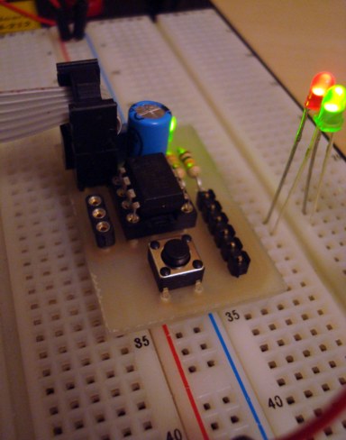
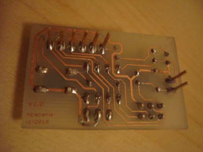
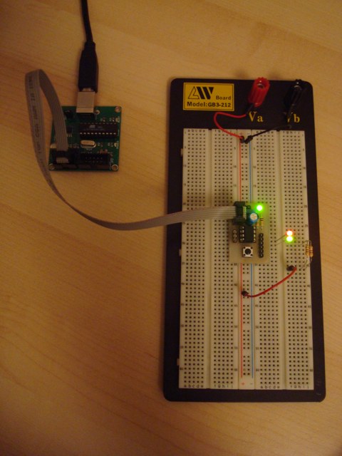
This handy breadboard header for ATTiny 25/45/85 microcontroller is a new design based on the original idea from Tinkerlog. Maybe the most useful feature is that it can provide power to the vertical breadboard strips while connecting all six port pins to the horizontal strips. Other features are :


  • 6-pin ISP connector (works great with USBtinyISP programmer)

  • easily accessible reset button
  • header for optional ceramic resonator

  • power led indicator

  • smoothing caps

Measuring approx. 4 x 2.5 cm (1½ x 1 in) is a great addition to your breadboard projects saving lots of extra connections.

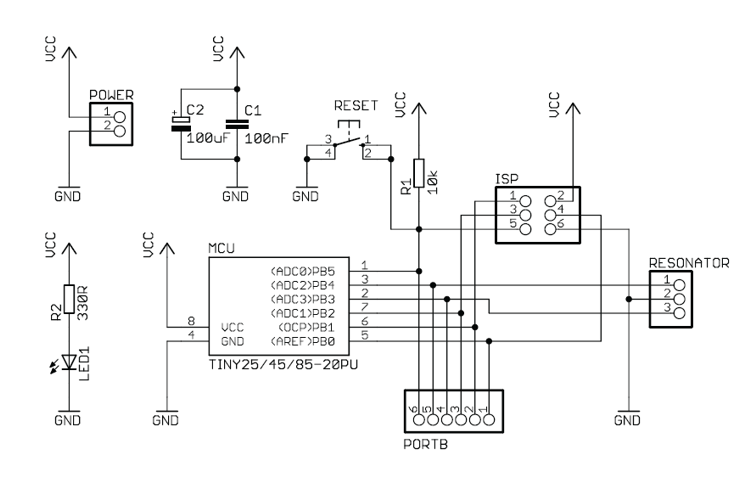
Schematic

Schematic

Bill of materials

R1                       10kΩ

R2                       330Ω

C1                       100nF

C2                       100uF/16V

LED1                  Green 3 mm

Button                  Omron type button
Headers               1×2, 1×3, 1×6, 2×3

IC Socket            8 pin

MCU                   ATTiny 25/45/85 PDIP

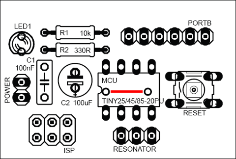
Don’t forget to solder the wire link under the IC socket (red line) !

Silk

1

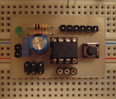
Photo of PCB – parts side

Photos

2

Photo of PCB – copper side

3


89Sxx Development Board

photo_1

Single side development board with In System Programmable Flash based microcontroller, 89Sxx series.

Introduction

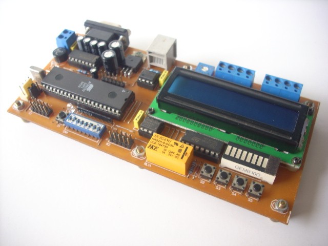
There are some 89Sxx development board, here is another one. I have designed this single side development board to be used as a tool for learning MCS-51 Microcontrollers, and for easy microcontroller project development.

The 89Sxx development board features :

  • 89Sxx 40-DIL based design, 89S51/52/53

  • In System Programming (ISP) through the 6-pin header

  • RS-232 and RS-485 serial port (shared pin) for communicating with serial devices like PC

  • HD44780 compatible alphanumeric LCD connectivity with backlight control

  • 4 on-board tact switch

  • 16 general purpose IO port pins on 5×2 header (Port0 and Port2)

  • 24Cxx I2C EEPROM

  • DS1302 serial Real Time Clock (RTC) with battery backup

  • On-board supply rectifier and voltage regulator

  • Single sided PCB design

Hardware

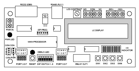
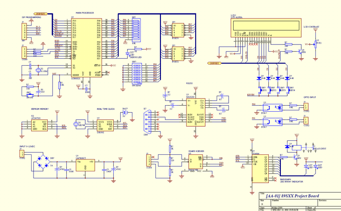
The hardware block is shown in Figure 1. The MCU is 89Sxx microcontroller. And the complete hardware schematic is shown in Figure 2.

  • Port1 is used as data-bus for LCD (4-bit interface, PCB lay-out for 16×2 character with backlight), on-board tact switch and connection for In System Programming (ISP)

  • Port0 and Port2 as general purpose IO, are available for interfacing external devices. Port0 is connected with DIP switch, and also P0.0 and P0.1 are connected with opto-isolated input

  • Port3, P3.0 and P3.1 are being used for serial communication UART, P3.2 for RS-485 control direction. P3.3 and P3.4 are serving as general purpose IO port pins. Another pins for communicating with serial chip, EEPROM, RTC and serial shift register (LED array indicator)

image_1

Figure 1. Hardware block of the 89Sxx Development Board

image_2

Figure 2. Schematic

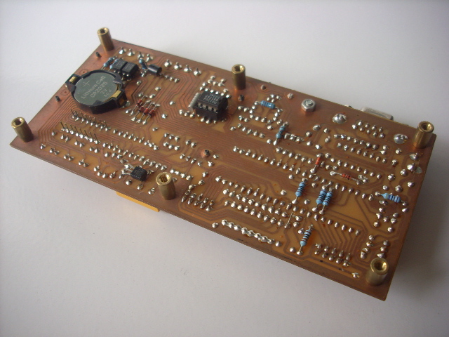
photo_2

Figure 3. Hardware

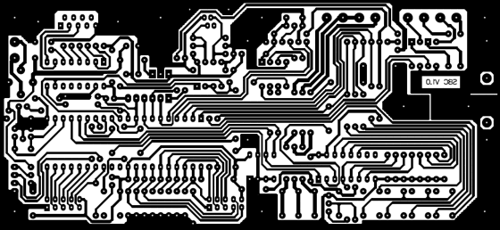
image_3

Figure 4. Printed Circuit Board

A SPI In system Programming adapter should be used for programming the circuit. Connect the ISP adapters 6 pin connector with the 6 pin ISP header on this board. Please note with the connection order (may a little bit different).

Example project … 89Sxx based SMS Controller

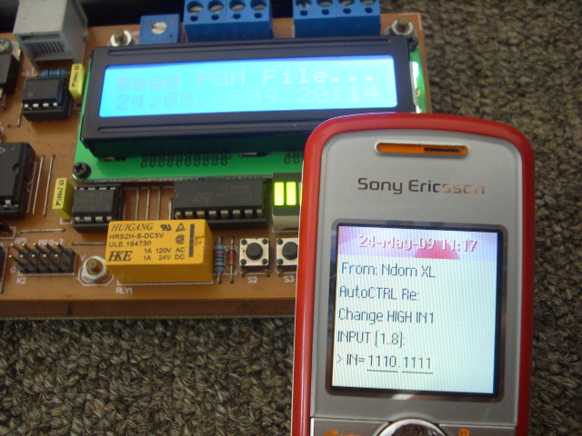
The project shows 89Sxx Development Board for remote control and monitoring. The system consists of 89S52 as main processor and mobile-phone (GSM modem) for remote control or monitoring over cellular network.
Features of the system are as follows.

Features of the system are as follows:

  • 8 ch input (Port0) and 8 ch output (Port2)

  • auto-send message on input changing/alarm, input changing mode : LO-HI, HI-LO

  • switch output command by group or independently

  • status request parameter by sending SMS command

  • download some simple text script for time programmable output

This circuit connects to the serial port featured by many cellular phones. Its function is to provide an input and an output port capable of being remotely controlled using another mobile.
Control takes place by means of sending SMS (Short text Messages Service). When the mobile receives a predefined text message, the circuit automatically recognizes it as a command, and switches the output accordingly.

The device can be used to notify the status of the input port, sending automatically a message every time the input changes. To know input status at any time, the device can send back a SMS describing the status of the input, as a response to a request message.

Communication between board and mobile-phone (modem) : rxgsm (P3.3 , RX from gsm), txgsm (P3.4 , TX to gsm) in TTL level. To start interfacing with, similar to modems, GSM cellular phones can accept AT commands(more precisely an extension of the AT command set).

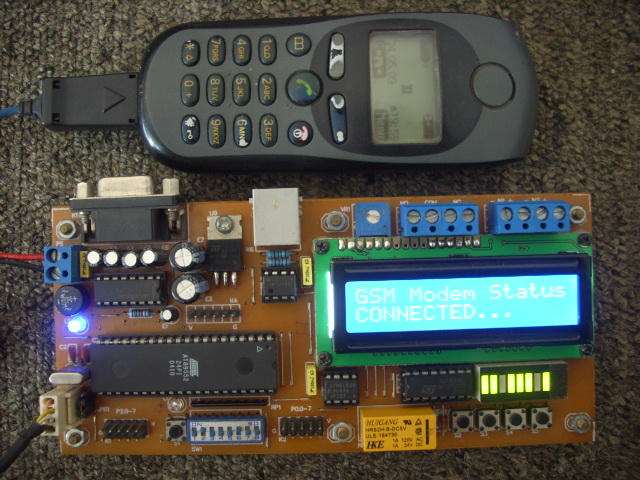
photo_3

photo_4

Figure 5. SMS Controller Project

MCU controlled Bluetooth automation with infrared sensor

image_1

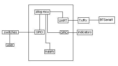
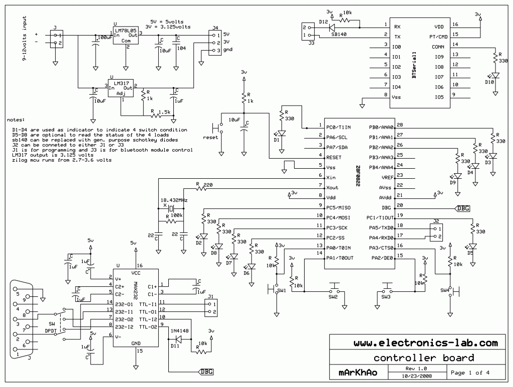
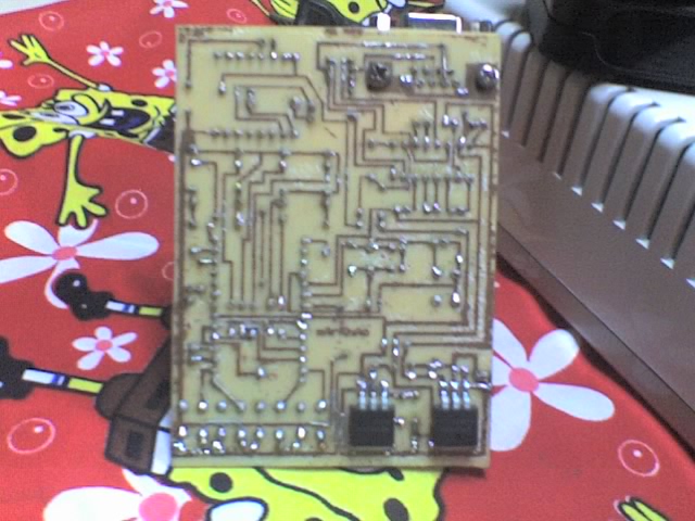
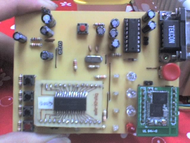
The microcontroller used is 0822 zilog encore! 8k series (soic,28pin) as shown on the figure. Is a programmable microcontroller, the functions used are the GPIO and the UART of the chip. GPIO is used on led indicators, and the UART is used for giving and reading AT COMMANDS to control the Bluetooth device.

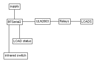
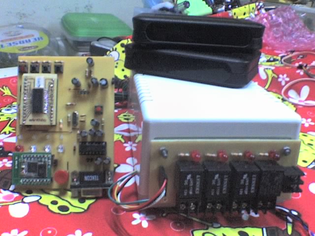
The whole process of the circuit, is to control the remote device using the 1st board (controller board), to switch a certain load on/off vice versa. Figure 1 explains how to use the controller and figure 2 explains how it functions according to the user. The user will enable the switches for the loads, then the mcu will give commands to the Bluetooth serial, then the remote device will receive the data, to enable the load.

image_2

figure 1

image_3

figure 2

Controller board

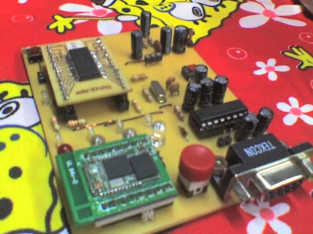
The controller board consists of the Bluetooth device, 0822 zilog encore, the max232 IC for programming, DB9 connector and some components, this board has a built in programmer, so it can be re-programmed any time the user wants to.

schem_of_controller_board

click for high resolution image

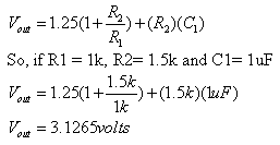
D9 and D10 is used to indicate connectivity from the other Bluetooth module(the remote device), it should be in the on condition. If it is not, the reset button can be pressed to make a new connection to the remote device. The max232 IC from maxim, is connected to a switch(DPDT, to make it much more cheaper), for either programming or serial communications in the hyperterminal of the PC. D1-D4 is used to indicate the switch status. D5-D9 is optional, it can be used to indicate the status of the load in the remote device, so the programming will be that easy. The power supply of the controller board consists of 3.1265 volts(LM317) and the LM7805 ic. Vout of the LM317 IC can be achieved by the formula:

image_8

controller_circuit2

Controller board (1st board)

Remote device board

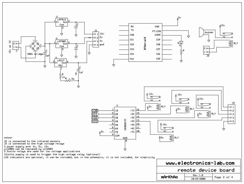
The main function of the remote device is to accept commands from the BTSerial1, or the controller board, via Bluetooth communications. This will turn ON/OFF the loads that is connected to the relays.

schem_of_remote_device_board

Schematic of the remote device board

The whole schematic is included in the rar file, so it will be easy for the others to see the whole schematics.

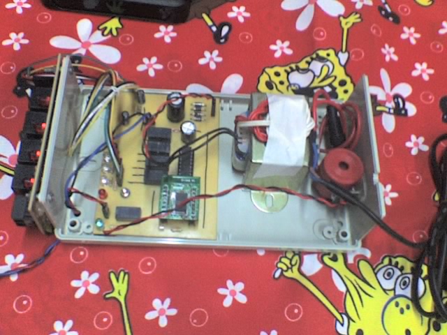
whole_remote_device

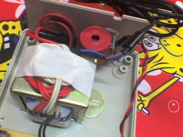
A shot of the whole circuitry of the remote device which includes buzzer, the power supply, the remote device board and the relay drivers for high voltage loads.

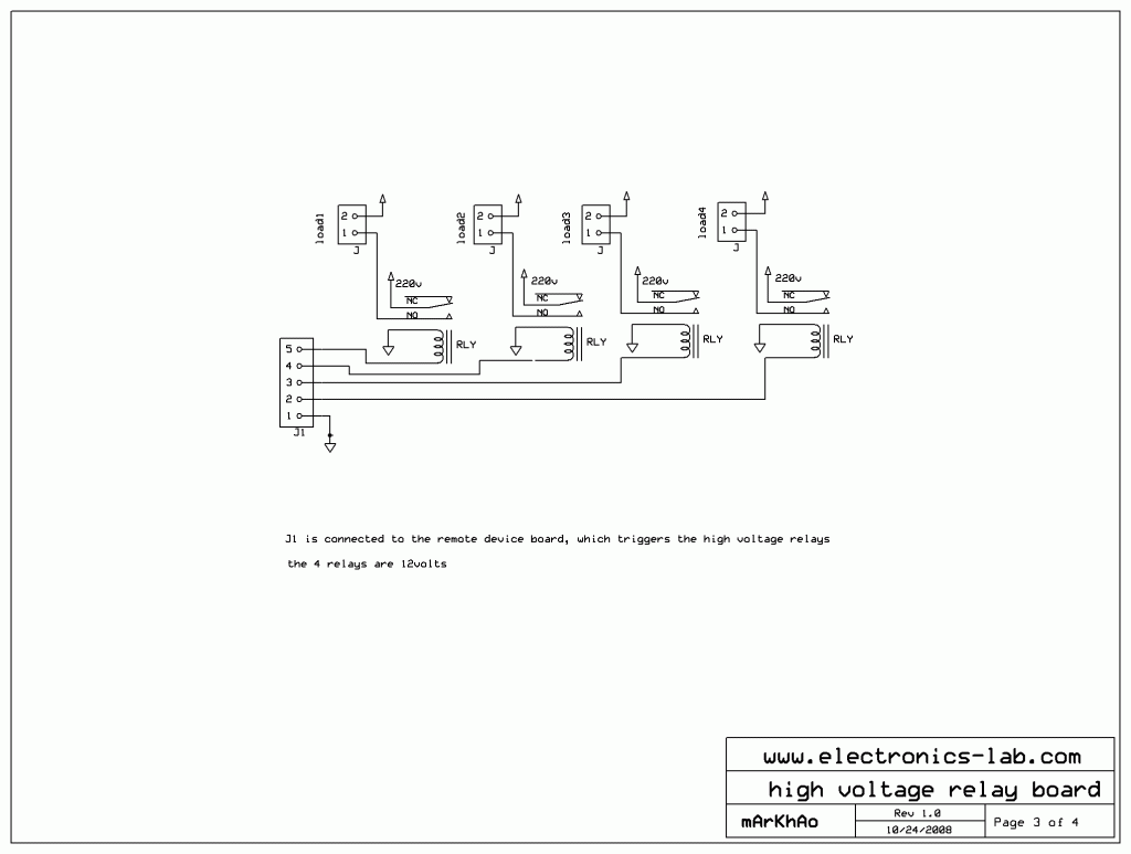
Relay board

The function of this relay board is to switch the high voltage loads(220volts), from low voltage signals.. this is connected to the remote device board.

schem_of_relay_board

click for high resolution image

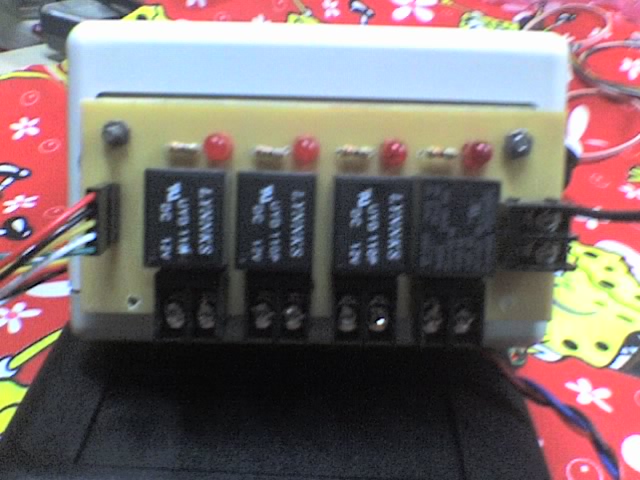
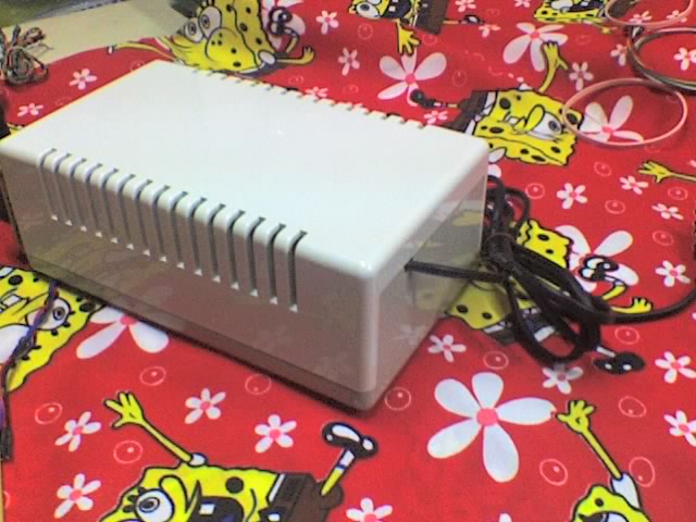
front_panel

The front panel, with 12volts relay to switch high voltage loads.

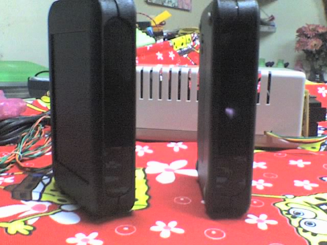
Infrared sensor

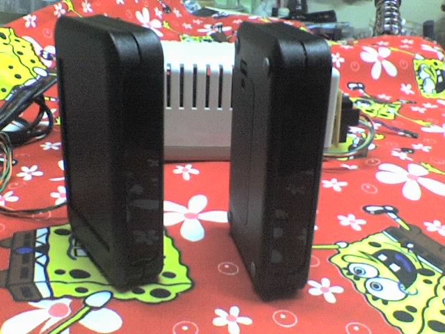
The infrared switch can be used as an alarm to intruders at home. The circuit and the pictures of the sensors, with buzzer are shown below

infrared_is_on

Infrared casing

sensor_case

Infrared is on, not visible to the human eye

with_buzzer

With the buzzer

image_4

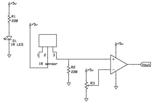
The circuit of the op-amp, using a simple comparator. To drive a relay, which will also drive the 12volts buzzer. buzzer The infrared switch can be used as an alarm to intruders at home. The process of the whole circuit is like a simple switch, but uses infrared, that, If the signal from the infrared transmitter is blocked, the buzzer will turn on, this will serve as a simple alarm that can have many useful applications. The whole circuit components are soldered directly, without PCB.

Photos

back_picture

bottom_pcb

controller_circuit

whole_prototype

Digital Volt and Amp Meter with Temperature Control

PSU_PRO_2

Introduction

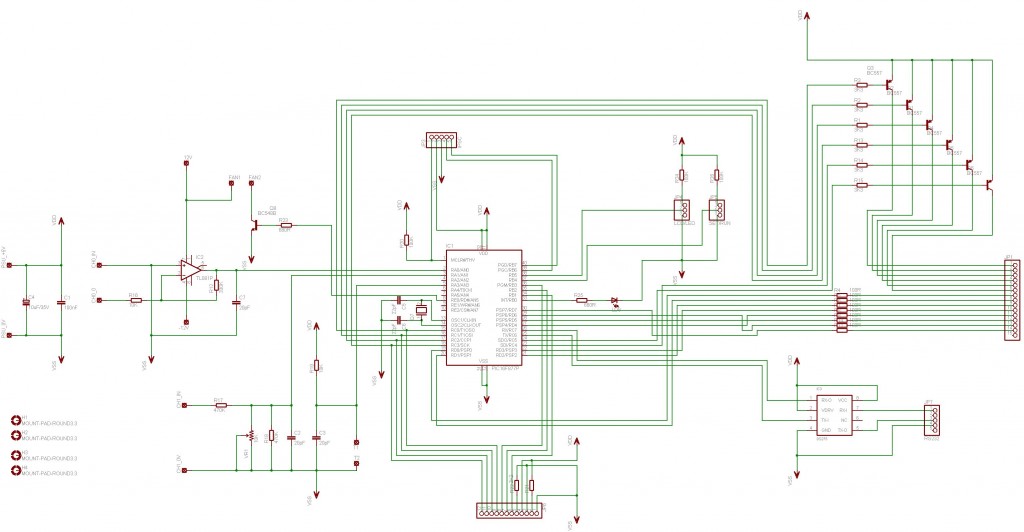
This project was designed and constructed as enhancement to the 0-30V Stabilized Power Supply Project with the DIY electronics hobbyist in mind. The circuit uses a single PIC Microchip to perform the Voltage, Current and Temperature conversions and display functions. The PCB Board uses large tracks and can easily be made using the “press-n-peel” method and a hobby drill. Components should be readily available anywhere in the world. Furthermore the hex files are available for the PIC16F877A and the PIC16F887 and the display can either be LCD or LED.

Proc_complete_for_LED

Warnings

There is only one warning – do not attempt to construct this project unless you are sure what you are doing. Nobody else but you can make the decision to construct it and therefore you are solely responsible for what you are doing or not doing with it.

Programming

The PIC Microchip Processor must be programmed before it will function as a Volt & Amp meter. There are many internet sites and PIC programmers that you can use. I used a Microchip MPLAB ICD 2 during the project. You might need to made changes to the circuit to accommodate a different type of programmer, do read the programmers instructions carefully.

Specifications

The circuit relies on the internal analogue to digital converter (ADC) of the PIC Microchip Processor. The accuracy is dependant on scaling the input voltage for the ADC for all three measurements. The good news is that both the PIC’s which can be used for this project have 10-Bit resolution ADC units which should work adequately in most circumstances.

In order to determine the resolution, simple to advanced mathematics can be used – I will use simple mathematics and present a basic explanation in order for you to get going on the project.

The Voltage of the PSU can be adjusted from 0 to 33V depending on the components in your circuit. The PIC can only measure voltages between 0 – 5V and represent the values measured as a 10bit binary number from 0 – 1024. In order to determine the voltage increments which can be measured one has to divide the scaled input voltage by 1024 and that equals: 33V/1024 = 32.2mV.

Similarly the current range is 0 to 3A. Which means that we can measure in 3.0/1024 = 2.9mA increments in a near perfect circuit.

Best Voltage resolution at 33.0V – 32.2mV
Best Current resolution at 3.0A – 2.9mA

Features

Either a LED or LCD display can be used:

  • LCD Output is compatible with most LCD Displays with a HD44780 drive chip, it was designed for a 2 line x 16 character display
  • 6 x 7 Segment LED Display using Common Anode displays
  • Configuration via RS232 terminal to set Voltage and Current conversion factors
  • Two PIC16F processors are supported, the 16F877A and 16F887 – separate hex files provided for download here
  • IPSC Connector for Programming the PIC in circuit
  • Separate -12V – 0 – +12V, Power Supply

Schematic Diagrams

Processor_1L

Processor

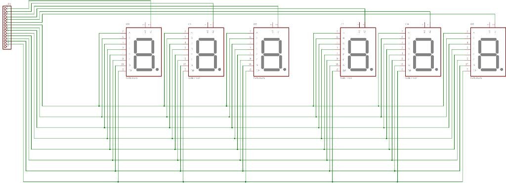
LED_1L

LED Display

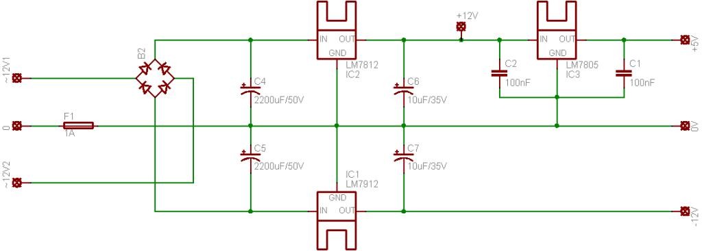
PSU_Schematic

PSU Schematic

The power supply requires a small 12-0-12 transformer not shown on the schematic. The circuit draws around 100mA. I used a 10VA transformer – please adjust the value of the fuse to project your transformer. The heatsinks had a SK145-25 part number on the packet, I am not sure if it is easily available.

Theory

Voltage

R17 and VR1 form a voltage divider as input to the ADC Input of the PIC. As the input voltage changes, so will the output of the Voltage divider on PIN 3 of the PIC. When calibrating the project for use it is important to remove the PIC from the circuit and adjust the Value of VR1 in such a manner that the output of the Voltage divider is never greater than 5.0V. Failing to do so might damage the PIC.

Current

The current measurement is more complex and involves an Op-Amp configured as an inverting amplifier to provide the input for the PIC. The resistor R7, in the Power Supply circuit is used as a shunt resistor. The small voltage drop across the resistor varies according to the amount of current a given load will draw from the PSU. In order to measure with greater accuracy the small voltage drop is amplified using an Op-Amp circuit.

Using the formula for an inverting amplifier the output voltage of the Op-Amp can be calculated as follows:

1. The maximum current through R7 maybe 3.0A
2. The voltage drop over R7 = V = I * R = 3.0A * 0.47R = 1.41V
3. Op-Amp output = Vout = -(R12/R16)(Vin) = -(33K/10K)/1.41V = -4.653V. However, the input is a negative voltage and if we negate the answer we should measure close to 4.653V for the maximum load.

Fan Control

For cooling the main heatsink a third channel on the PIC’s ADC is used to measure the temperature and control a small fan. For this purpose a NTC Thermistor with a value of 10K is used. The NTC Thermistor is a device which reduces in resistance as the temperature increases. The same principal of a voltage divider is used to produce a voltage output which will allow the PIC to be used to determine the temperature measurement. The NTC Thermistor is connected in series with a 10K resistor R19 to produce a variable voltage output the PIC will compare to a setpoint to determine if the fan will be switched on.

Electrical Setup

It is highly recommended to use IC sockets on the PCB. This will greatly assist with setting up the project.

Voltage:

Remove all the ICs from the PCB
•Adjust the PSU for the lowest output 0V
•Adjust VR1 to its middle or halfway position
•Connect the Voltage inputs CH1_0V and CH1_IN to the output of the PSU.
•Connect a DVM to the 0V and PIN 3 of the 40 PIN IC socket
•Adjust the output of the PSU and follow the increase and decrease of voltage on the output of the voltage divider
•Adjust the PSU to deliver this maximum output
•Now adjust VR1 to until the DVM measures 5.00V at the maximum output of the PSU

Current:

Remove all the ICs from the PCB
•Connect a dummy load to the PSU, for calibration I used a 12V globe drawing 690mA
•Now connect the DVM to the CH0_0 and CH0_IN connections
•Add and remove the dummy load and note down the increase and decrease in the voltage drop over R7 and the inputs of the Op-Amp. CH0_IN should measure negative in respect to CH0_0.
•Now insert the OP-Amp into the IC socket and apply the power to the processor board from the -12 – 0 – +12V PSU
•The output of the Op-Amp PIN 6, must have a positive voltage with the dummy load connected and should be close to the value calculated as follows:

  • As an example, I will use the 690mA 12V globe.
  • Voltage over R7 = (0.69*0.47) = 0.3243V
  • PIN 6 V (out) = (33K / 10K) * 0.3243V = 1.070V
  • The exact Voltage is not important, as long as it is close to 1.070V and drops to 0V when the dummy load is removed.
    • Ensure the output voltage of the Op-Amp is present at PIN 2 of the 40 PIN IC socket

Temperature:

Connect the power to the processor board from the -12 – 0 – +12V PSU
•Now connect the DVM to Vss (0V) and PIN 5 of the 40 PIN IC socket.
•Heat and Cool the Thermistor and ensure a voltage drop decrease or increase is present on PIN 5.
•There is no adjustment required for the Thermistor.

Software Configuration

The project needs to be calibrated before use and the following instructions must be followed carefully. A software terminal emulator is required and I suggest RealTerm available from ( http://realterm.sourceforge.net ) . Please do not use Hyperterminal – it does not work for this project.

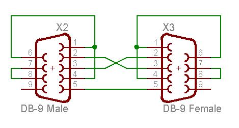
A null-modem cable is required to ensure correct handshaking and the pin-outs are as follows:

Cable_1

X2 – To project board
X3 – To PC or Terminal

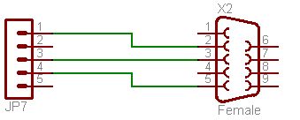
From connector X2 you need to make a Pigtail adapter:

Pig_Tail

X2 PIN 2 connects to JP7/1
X2 PIN 3 connects to JP7/3
X2 PIN 5 connects to JP7/4 (Vss)

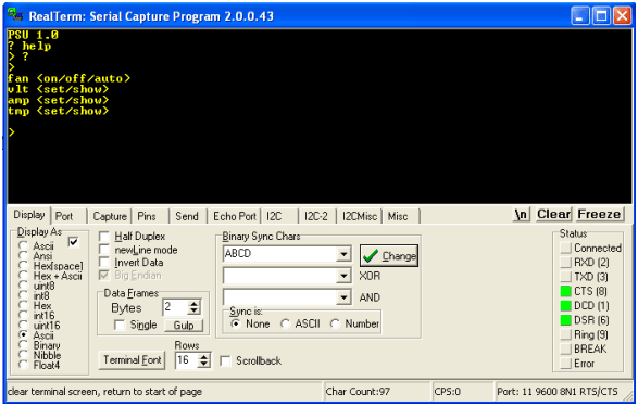
RealTerm_1

Port Configuration

Determine the serial communications port you are using and start realterm with the following command line parameters:

realterm.exe baud=9600 port=xx flow=2

or if you are using a different terminal use:

9600, none, 8, 1, rts/cts flow control

  • Enable the setup mode by placing a Jumper on JP5 on the SET position
  • A question mark <?> will show some help with the commands
  • Power up the processor board and you will receive the following messages and follow the example shown:

RealTerm_2

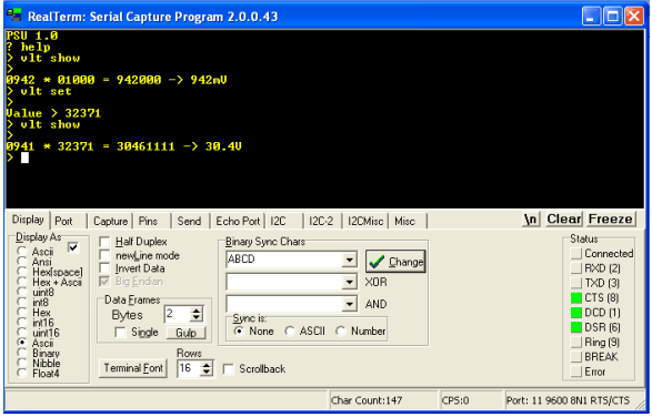
Voltage Calibration 

  • Connect the DVM to the output of the PSU and adjust the output to the maximum output voltage e.g. 30.1V
  • Type the command >vlt show

You will see something like the following on the terminal console:

0960 * 01000 = 960000 -> 960mV

The second value <01000> is the value you are interested in and this value may be changed to suite your needs.

      Example:

  • To adjust the display output to 30.1V take the following steps
  • Divide 30.1V by 960 = 0.032533748
  • Multiply the answer by 1,000,000 = 3253
  • Type the comman >vlt set
  • At the prompt enter the value e.g Value >32533
  • Now type the <vlt show> command again to see the result.

RealTerm_3

Current Calibration

  • Connect the DVM in series with a small load (e.g. 12V Globe) to the output of the PSU and adjust the output to limit the current value  e.g. 500mA
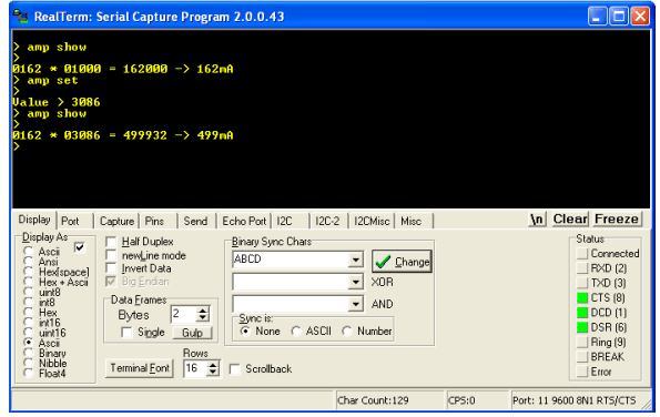
  • Type the command >amp show

You will see something like the following on the terminal console:

0162 * 01000 = 162000 -> 162mA

The second value <01000> is the value you are interested in and this value may be changed to suite your needs.

  • Example:
  • To adjust the display output to 500mA take the following steps
  • Divide 500 by 162 = 3.086
  • Multiply the answer by 1,000 = 3086
  • Type the command >amp set
  • At the prompt enter the value e.g Value >3086
  • Now type the <amp show> command again to see the result.

Temperature and Fan

  • Type the command >tmp show

You will see something like the following on the terminal console:


0395 – 0400 – 0001


The first value is the raw ADC value, the second is the temperature set point and the third is the value of the fan timer. You can adjust the set point value to suite the type of NTC Thermistor you are using.


  • The fan must be set to “auto” for this setting to work by using the <fan auto> command.
  • The fan will switch on when the ADC value is below the set point and switch off when the ADC value is higher than the set point and the fan timer has reached a pre set value. This will prevent the PIC controlling the temperature of the Thermistor to a pre set value.


  • The timer value can not be adjusted – I have used <4096kb> program memory. However a US$69.00 license will remove the memory limitation and enable a future <4096kb> memory to code up to. Any enhancements will have to wait until I can afford the upgrade.

LCD Connection

JPL LCD ATM1602B Connections

RS to RB5 – PIN 38
R/W to RB4 – PIN 37
E to RB3 – PIN 36
DD0 to None
DD1 to None
DD2 to None
DD3 to None
DD4 to RD4 – PIN 22
DD5 to RD5 – PIN 21
DD6 to RD6 – PIN 20
DD7 to RD7 – PIN 19

Parts

 The board may be used in various configurations and some parts are not required when an option is selected.

The PIC16F887 does not require the following parts:

Q7 – 4.0MHz crystal

C5, C6 – 22pF Ceramic Dipped Capacitor

The LCD Display Option does not require the following parts:

R4, R5, R6, R7, R8, R9, R10, R11 – 100R Resistors

R1, R2, R3, R13, R14, R15 – 3K3 Resistors

Q1, Q2, Q3, Q4, Q5, Q6   – BC557 PNP Transistors

LD0, LD1, LD2, LD3, LD4, LD5 – 7 Segment Displays

For some parts you need to calculate a value:

R22 – Current limiting resistor value for LCD Backlight

Qty Value Device Parts
1 PIC16F877A/887 PIC Microchip IC1
1 3mm LED LED1 LD6
1 LCD Backlight R 21
1 4.0MHz XTAL/S Q7
1 2K2 Calculate .25W Resistor R 22
6 3K3 .25W Resistor R1, R2, R3, R13, R14, R15
2 10K .25W Resistor R16, R19
1 10K TRIMPOT VR1
1 10uF/35V Elect Cap Radial C4
3 20pF Ceramic C2, C3, C7
2 22pF Ceramic C5, C6
3 100K .25W Resistor R20, R24, R26
8 100R .25W Resistor R4, R5, R6, R7, R8, R9, R10, R11
1 100nF Ceramic C1
1 330K .25W Resistor R 12
2 470K .25W Resistor R17, R18
2 680R .25W Resistor R23, R25
1 BC548B BC548B Q8
6 BC557 BC557 Q1, Q2, Q3, Q4, Q5, Q6
1 DS275 DS275 IC3
1 IPSC 1X5 Socket JP3
1 LCD/LED 1X3 Pin Header JP4
1 SET/RUN 1X3  Pin Header JP5
1 RS232 1X5 Socket JP7
6 SA56-11SRWA Kingbright LD0, LD1, LD2, LD3, LD4, LD5
1 TL081P TL081P IC2
1 Ampron MF11 Thermistor 10K TH1

Lastly

Never give up hope. I destroyed 3 PIC Processors, 2 x 1.6A Fuses, 1 x 5V6 Zenner diode and one Fluke 630mA fuse while developing this project. I made three sets of PCB Boards and redesigned the 12/-12V PSU twice. I was ripped off when I purchased 20 bad quality 2200uF/50V capacitors. When I got stuck I asked for help and got it – thanks to Audioguru at electronics-lab for assisting me.

Photos

Picture 049

Picture 050

Picture 052Picture 055Picture 056Picture 063

AquaCont – Aquarium Control

Prototype1

The experimental circuit

The AquaCont is an electronic system witch permits to manage and to monitor most of the parameters of all the electrics devices that can be found in a aquarium. The PIC18F4520 used to realize it, combines a real time clock and a temperature sensor in order to control 8 relays. The system main characteristics are:

  • time / calendar

  • weekly timer for 6 daily events

  • digital temperature sensor

  • additional eeprom memory

  • 8 outputs controlled by relays joinables to timer events ( 2 of them that can be joined to temperature sensor)

  • LCD display 4×20

  • 8 bicolour LEDs associated to output ports

  • RS232 serial port for PC communication

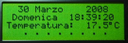
The LCD display permits to monitor the current date and time, the temperature detected by the sensor and moreover it permits to visualize each port status in the last row. In the following LCD screens display it is possible to program the weekly timer events, set the temperature sensor parameters and manage the serial connection with a PC where is running the included WinTimer software.

The power supply needed by the main board is 5V, while the relays board requires 12V; the different source power was useful in granting the protection of the microcontroller and his circuits from overvoltage and short circuit on the 220V. Two optocouplers are utilized for that purpose ensuring the isolation of the different voltages.

main_screen

Fig.1 – Main screen

The weekly timers are programmed basing on the clock provided by the proper integrated circuit supplied with a lithium battery. The timers data are memorized in the micro’s eeprom. The RS232 serial port allows to simply program the micro using the corresponding PC software; the functions provided in the PC software are also included in the firmware, except for the PC clock syncing. Using the Pc software is also possible to assign a description, to each of the 8 relays ports that will be memorized in the additional LC2416 eeprom memory. In this memory will be also stored the temperature sensor’s settings data.

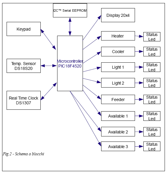
Block diagram

The following figure shows the block diagram of the system.

diagramm1

Fig.2 – Block diagramm

Schematics

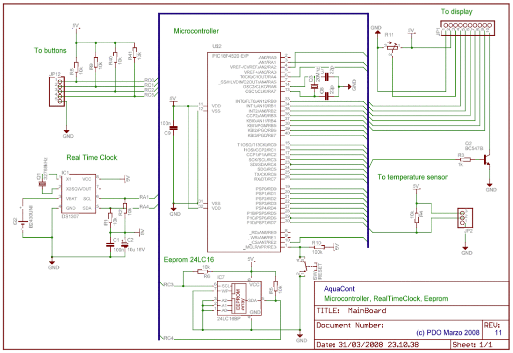
schematic0

Main schematic

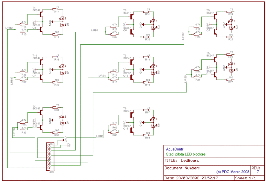
schematic1

Led board schematic

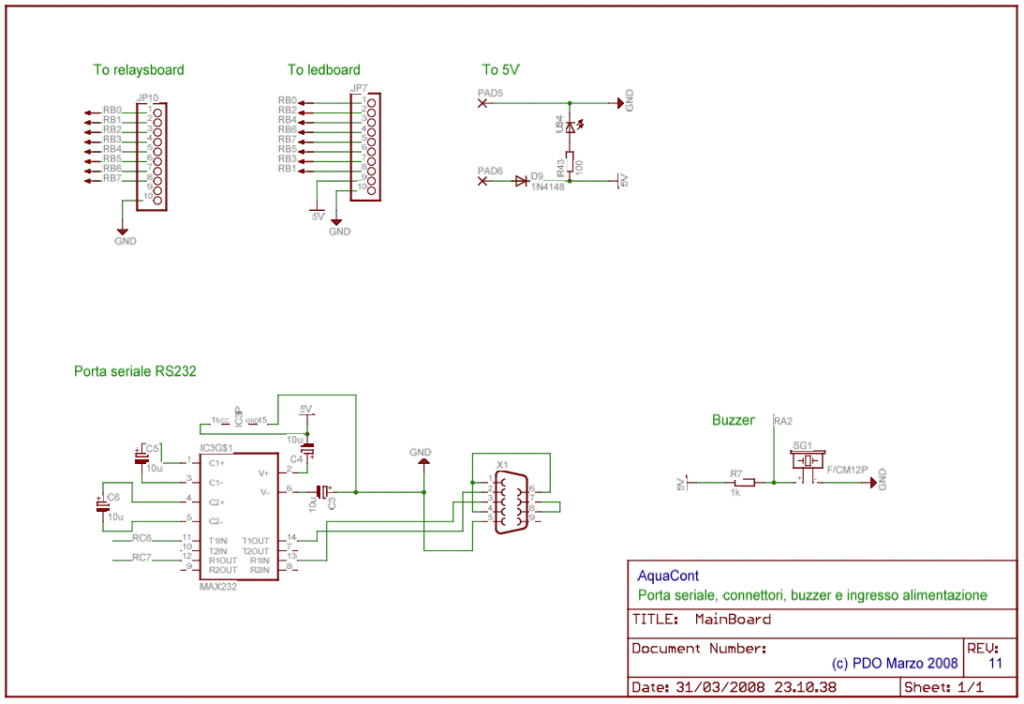
schematic2

Main board schematic

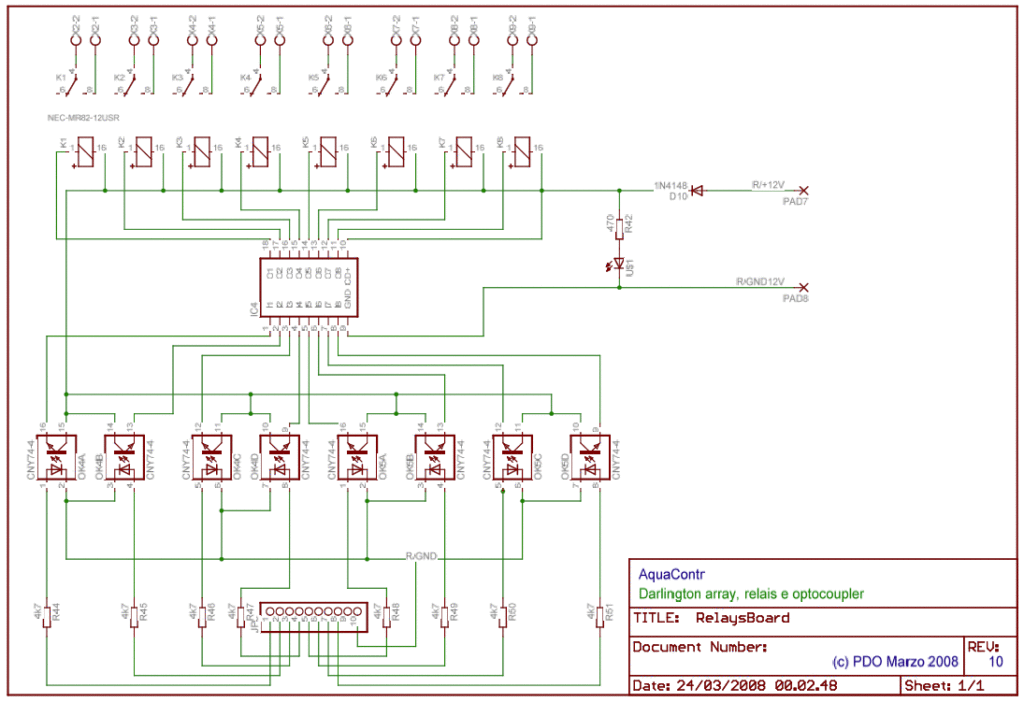
schematic3

Relays board schematic

Firmware’s notes

The mikroC language is known for its large functions library and for its good development board so it was used for developing the AquaCont firmware. In fact the first AquaCont prototype was developed using the MikroElektronika’s EasyPIC4 and two breadboards. Please note that the firmware’s source code can be recompiled only using a registered version of MikroC compiler, while the freeware version limits its output to 2K program words.

The AquaCont firmware was conceived from the idea of A. Di Stefano’s “macchina a stati”, published in his article “Realizzazione di un timer digitale programmabile“ on the 257n of the “Fare Elettronica” Italian magazine; the original code was obviously modified for making it compatible with the new hardware and new needs. In the new code have
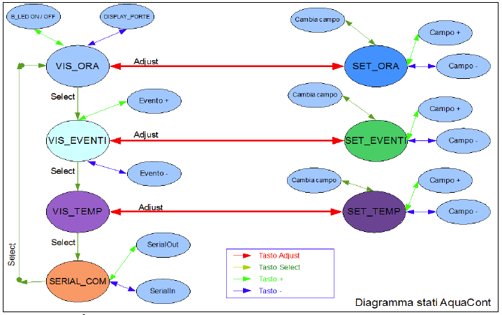
been implemented some new I2C functions for the communication with the Dallas RTC DS1307, the temperature sensor Maxim DS18S20, the eeprom memory 24LC16 and, using the USART functions library, for the RS232 serial port.  The original idea of a states structure remained unchanged even if it was implemented with new functionalities and at the same time, updating those already existing. In Fig.4 it is shown the states diagram structure. The stato variable determines which one of the seven function will be executed in the main loop. Every single function is independent and permits to modify the state in relation to the pressed button.

diagramm2

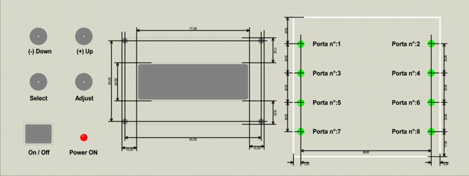
Front Panel

AquaCont-V1

Photos

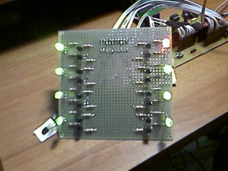
LedsBoardProto

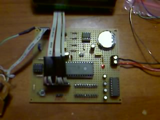
MainBoardProto

MainBoardProto_Rear

Prototype2

RelaysBoardProto

Download Full project in ZIP (including schematics, boards, firmware ENGLISH and SPANISH, software).


EPROM adapter for ATMEL 89 Series Flash Microcontroller

sch

Devices

The EEprom programmer software supports the following devices.

28C16 28C256 28C17 29C256 28C64

Hardware

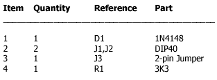
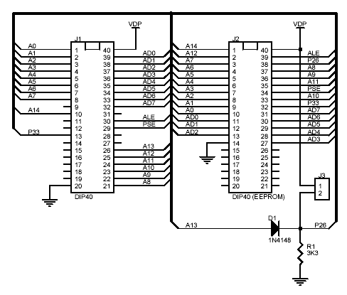
Diode D1 and resistor R1 provide the VDD isolation when programming the 24 pin devices. The jumper J3 must be shorted for 24 pin devices, and open circuit for 28 pin device programming. Following EEPROMs are pin compatible with their EPROMs version,

28C16 —> 2716

28C64 —> 2764

29C256 —> 27256

The software for this adapter is located here: http://chaokhun.kmitl.ac.th/~kswichit/E2RomPgm_web/PgmE2w.zip

Parts

parts


TOP PCB Companies