RoomSense IQ is a smart sensor that can detect human activity using millimeter-wave Radar

RoomSense IQ sensor

RoomSense IQ is a smart sensor that can detect motion, temperature, humidity, and light levels. It is designed to be placed in any room in your home, and it can help you keep track of the temperature, humidity, and light levels in each room. It can also help you monitor the activity in your home by detecting motion.

The hardware platform uses millimeter-wave radar technology and PIR sensors to detect and measure the movement of individuals in a room. RoomSense IQ features a temperature and humidity sensor for monitoring indoor climate. It also has an ambient light sensor for the control of lights. All this information can be accessed in real time via the Home Assistant dashboard.

Inside the RoomSense IQ is the Espressif ESP32S3 microcontroller with Wi-Fi wireless connectivity. The board includes a USB Type C port for power and serial communication, allowing customers to connect the sensor to a computer for local controls.

RoomSense IQ also has a number of customizable settings. You can set it to alert you when certain conditions are met, such as when the temperature in a room gets too high or too low. You can also set it to turn on lights or other devices when motion is detected in a certain room.

The onboard PIR sensor is also used to reduce false alarms as it is designed to filter out non-human activities. This allows the hardware device to differentiate between human and non-human activity inside the room and only trigger when necessary.

RoomSense IQ is designed to be user-friendly and easy to set up. You simply use the Home Assistant platform through the MQTT protocol. The system provides an open-source dashboard to view real-time data in eight distance bins, including macro and micro energy levels. The app provides step-by-step instructions on its GitHub repository.

In conclusion, if you’re looking for a smart sensor that can help you keep track of the activity and environment in your home, then RoomSense IQ is definitely worth considering. Its customizable settings make it a versatile and valuable addition to any smart home setup.

Vodafone’s 5G network on a modular Raspberry Pi based hardware

Vodafone prototype 5G network built on a Raspberry Pi computer

Vodafone, one of the leading telecommunications companies in the world, has recently announced the development of a prototype 5G network built on a Raspberry Pi computer. The Raspberry Pi is a low-cost, credit card-sized computer that is commonly used for educational purposes and prototyping.

The development of this 5G network prototype on such a small and affordable device is significant because it demonstrates that the technology required for 5G networks is becoming more accessible and affordable. This could potentially open up opportunities for smaller companies and organizations to experiment with and implement 5G technology in their operations.

“Whilst this is just a prototype, it has the potential to bring new cloud, AI, and big data technologies within reach of many of the small businesses we support across Europe. The next step is to take ideas like this to a place where they can be developed and eventually produced. Our door is open to interested vendors,”

said Santiago Tenorio, Vodafone’s Director of Network Architecture.

The prototype 5G network built on the Raspberry Pi uses open-source software designed to be modular and scalable. This means it can be easily adapted and modified to meet the specific needs of different applications and industries. The network prototype also includes a cloud-based mobile edge computing (MEC) platform, which enables low-latency processing and data analysis at the network edge. This could have significant implications for industries such as healthcare, where real-time medical data processing is critical.

Vodafone’s development of this prototype 5G network is part of its broader efforts to accelerate the adoption and deployment of 5G technology across its networks. The company has already launched 5G networks in several countries and is investing heavily in developing and deploying 5G infrastructure. The development of this prototype network on a Raspberry Pi is just one example of the company’s innovative approach to 5G technology. It will be interesting to see how it is further developed and applied in the future.

Vodafone will be demonstrating its 5G solution based on the Raspberry Pi at the Mobile World Congress in Barcelona.

Qualcomm Aware platform combines edge computing and cloud technologies for IoT solutions

Qualcomm Aware

Qualcomm, the leading wireless technology innovator, announced the expansion of its offering by introducing a new suite of products and services called Aware. The new offering aims to simplify and accelerate the implementation of the Internet of Things (IoT) across various industries, including industrial, commercial, and consumer markets.

With the growing demand for IoT solutions, businesses face various challenges, such as device management, security, and connectivity. Qualcomm’s Aware platform addresses these challenges by providing a comprehensive solution that includes hardware, software, and cloud-based services. The platform leverages Qualcomm’s expertise in wireless technologies, artificial intelligence, and machine learning to provide businesses with a reliable and scalable solution.

The Aware platform includes various hardware and software components, including IoT sensors, gateways, and edge computing devices. These devices are designed to capture data from various sources, process it locally, and transmit it securely to the cloud for analysis. The platform also includes software tools that enable businesses to manage and monitor their IoT devices and cloud-based services for data analytics and machine learning.

//players.brightcove.net/1414329538001/BJv5wEFt_default/index.html?videoId=6320892259112

One of the key features of the Aware platform is its security capabilities. Qualcomm has integrated advanced security features into the platform, such as device authentication, encryption, and secure boot. These features ensure that the data collected by IoT devices are protected from unauthorized access and tampering.

Qualcomm has also designed the Aware platform to be flexible and adaptable to different business needs. The platform is compatible with various communication protocols, including Wi-Fi, Bluetooth, and cellular networks. This allows businesses to choose the best connectivity option for their use case.

In addition, the Aware platform is designed to be easy to use and deploy. Qualcomm has partnered with leading system integrators and solution providers to offer comprehensive support and services to businesses. This includes consultation, design, implementation, and ongoing support.

The Aware platform is available now, and businesses can visit the product page on Qualcomm’s website to learn more about the various components and services included in the platform. With the introduction of the Aware platform, Qualcomm aims to empower businesses to leverage the power of IoT and drive innovation across various industries.

Eoxys launches two machine learning modules for advanced IoT applications: Xeno+ Nano ML

Eoxys Xeno+ Nano ML

In today’s world, data is everywhere, and the need for data analysis is increasing rapidly. One of the most promising technologies to enable an intelligent analysis of data is Machine Learning (ML). Machine Learning has revolutionized many industries by helping them make sense of the vast amounts of data generated daily. However, building machine learning models requires expertise, infrastructure, and time. Eoxys has developed Xeno+ Nano ML, a powerful, easy-to-use, and cost-effective machine learning solution to overcome these challenges.

Xeno+ Nano ML is a machine learning solution developed by Eoxys, a leading provider of IoT and AI solutions. It is a complete end-to-end solution that helps developers build, train and deploy machine learning models quickly and easily. Xeno+ Nano ML provides a comprehensive suite of tools that make it easy to build and train ML models using various algorithms and data sources. It includes an intuitive web-based interface, pre-built models, and access to a vast library of machine-learning algorithms.

The Xeno+ Nano ML is designed to be flexible and scalable, allowing developers to customize it to their specific needs. It supports multiple platforms, including STM32 and Nuvoton, making it compatible with a wide range of hardware.

The Xeno+ Nano ML STM is the version of Nano ML that is compatible with STM32, a popular microcontroller used in embedded systems. The module is powered by the STM32L4 series Arm Cortex-M4 controller clocked up to a frequency of 80MHz. This is an excellent solution for developers looking to integrate machine learning into their existing STM32-based projects.

The Xeno+ Nano ML Nuvoton is based on the IoT microcontroller unit, Nuvoton Arm Cortex-M23 trust zone series clocked at a frequency of 96MHz. This module is ideal for a Trusted Execution Environment with Trusted Applications, featuring the security capabilities of TrustZone for Armv8-M technology.

Both modules feature Syntiant NDP120 neural decision processor that runs multiple audio and sensor applications with lower power consumption. The module also includes InnoPhase IoT’s Talaria TWO certified Wi-Fi and BLE module that provides integrated support for wireless connectivity.

The Xeno+ Nano ML is compatible with popular machine learning frameworks and supports multiple platforms, making it a flexible and scalable solution for a wide range of use cases.

STMicroelectronics unveils NB-IoT modules with GNSS and geo-location capability

STMicroelectronics, a global leader in semiconductor solutions, has recently launched its latest series of industrial modules for Narrowband Internet of Things (NB-IoT) applications, featuring advanced geo-location capabilities using Global Navigation Satellite System (GNSS) technology. The ultra-compact and low-power modules are designed to offer an all-in-one solution for industrial IoT applications, providing high performance and cost-effectiveness.

The new modules are part of STMicroelectronics’ extensive portfolio of wireless modules, designed to provide reliable and efficient connectivity for IoT applications. The modules combine the latest NB-IoT technology with GNSS positioning capabilities, allowing them to be used in various applications, including asset tracking, smart cities, and smart agriculture.

The modules are designed to operate in extreme temperatures and environmental conditions, making them suitable for use in various industrial applications. They also feature a low-power design, enabling them to be used in battery-powered devices for extended periods of time.

The ultra-compact size of the modules means they can be easily integrated into a range of devices, making them an ideal solution for developers looking to add connectivity and geo-location capabilities to their products. The modules are also pre-certified for use in various global markets, reducing development time and costs for developers.

According to STMicroelectronics, the modules are designed to offer a number of key benefits, including reduced time-to-market, improved reliability, and lower development costs. They are also designed to meet the demanding requirements of industrial IoT applications, providing robust and secure connectivity in challenging environments.

“NB-IoT is rapidly gaining momentum in industrial applications, driven by the need for reliable and efficient connectivity in challenging environments,” said Fabio Gualandris, Industrial & Power Conversion Division General Manager, STMicroelectronics. “Our new modules combine the latest NB-IoT technology with advanced geo-location capabilities, providing an all-in-one solution that meets the needs of developers and manufacturers looking to create innovative IoT products.”

The new modules are available for evaluation and sampling, with volume production expected to begin in the second half of 2022. With the launch of these new modules, STMicroelectronics is well-positioned to meet the growing demand for reliable and efficient connectivity in industrial IoT applications, providing developers with the tools they need to create innovative products that can deliver real value to businesses and consumers alike.

NGK Develops Evaluation System That Visualizes Remaining Battery Capacity of Li-ion Rechargeable “EnerCera” Batteries Together With onsemi

NGK INSULATORS, LTD. (hereinafter “NGK”) has developed an evaluation system that visualizes the conditions of Li-ion rechargeable “EnerCera®” batteries, including remaining battery capacity, together with ON Semiconductor Corporation (Headquarters: Arizona, U.S., hereinafter “onsemi”). Being able to assess the status of the battery will enable the efficient use of EnerCera.

The evaluation system is equipped with a battery sensing integrated circuit (IC) for monitoring the remaining battery capacity with high accuracy that onsemi has optimized specifically for EnerCera and ultra-low power consumption. In addition to remaining battery capacity, it enables the visualization of conditions such as voltage and temperature, which helps save power and extend the lifespan of devices and systems. The evaluation system also eliminates the need for verification of individual data of battery, which had previously been required to measure remaining battery capacity, and can verify items such as the load and stability of EnerCera while the device is operating, making it possible to reduce the duration of development of devices, etc. that use EnerCera. As part of development support, NGK will provide all customers that use EnerCera with reference designs and evaluation boards free of charge starting from November 2022 to improve development efficiency.

EnerCera is an ultra-small and ultra-thin Li-ion rechargeable battery. Through a semi-solid battery that uses NGK’s original Crystal Oriented Ceramic Plate as electrodes, NGK realizes characteristics sought in power sources for IoT devices such as high capacity, high output, high heat resistance, and a long lifespan, which were difficult to combine in conventional Li-ion rechargeable batteries.

EnerCera is currently being adopted in smart keys and smart cards, and sensor-equipped wearable devices, etc., and progress is being made on sample evaluations at over 500 companies worldwide. NGK will continue to develop and provide various power source solutions using EnerCera toward the popularization of IoT devices, and contribute to the development of a digital society.

Evaluation system with onsemi’s built-in battery sensing IC for monitoring remaining battery capacity

The UP Squared Pro 7000 Introduces MIPI CSI Camera Support, LPDDR5, and 1.4x the CPU Performance to the 4″ x 4″ Form Factor

AAEON produces the world’s first industrial motherboard with Intel® Core™/Atom®/N-Series processors (formerly Alder Lake-N).

AAEON, a leading manufacturer of AI development solutions, has released the UP Squared Pro 7000, bringing the acclaimed UP Squared Pro series into its third generation.

The UP Squared Pro 7000 sees dramatic improvements when compared to the boards preceding it. The first of these is that it is the world’s first industrial motherboard equipped with the Intel® Core/Atom®/N-Series processor platform (formerly Alder Lake-N), which offers 1.4x the CPU performance of the previous generation, alongside the benefit of supporting the Intel® Distribution of OpenVINO Toolkit. In addition, the board hosts 16GB of onboard LPDDR5 4800MHz system memory, doubling the bandwidth and data transfer speed of the previous model, while increasing overall energy efficiency.

A first for the UP Squared Pro product line, the UP Squared Pro 7000 supports MIPI CSI cameras via an FPC port, freeing up its two 2.5GbE (Intel® i226-IT) and three USB 3.2 Gen 2 ports for other peripheral devices. Developers also gain access to exceptional expansion from the dense, 4″ x 4″ (101.6mm x 101.6mm) board, with the same 40-pin GPIO header alongside M.2 E, M, and B Keys for CNVI, PCIe, and USB add-ons.

Another change likely to attract vision-intensive application developers is the board’s improved display interface, which boasts HDMI 2.0b and DP 1.2 ports and DP 1.4a via USB Type-C to achieve three simultaneous 4K displays. Combining this with Intel® UHD Graphics for 12th Generation Intel® Processors makes the board an excellent base for bringing intelligent factory robotics and digital signage solutions to market.

The UP Squared Pro 7000 also features onboard TPM 2.0, alongside OS support for Windows® 10 IoT Enterprise, Windows® IoT Core, Ubuntu 22.04 LTS, and Yocto 4; in addition to its support for the Intel® Distribution of OpenVINO Toolkit.

For more information about the UP Squared Pro 7000, please visit our product page or contact an AAEON representative directly.

Scintil Photonics demonstrates first single chip 100 GHz DFB Comb Laser Source at OFC 2023

High-performance computing and AI applications set to gain improved computing system performance and power efficiency through Scintil’s multi-port comb laser

Scintil will also present: ‘Fully Integrated III-V-on-Silicon Multi-Port DFB Laser Comb Source for 100 GHz DWDM’ during OFC, San Diego (CA), taking place March 5 – 9

Grenoble, France, March 1, 2023 – Scintil Photonics, a leading innovator in silicon Photonic Integrated Circuits (PICs), will demonstrate its latest technology, a single-chip multi-port 100 GHz DFB (Distributed FeedBack) Comb Laser Source for high-performance computing and AI applications, at booth #3351 during OFC 2023.

Named SCINTIL Comb Laser Source, this is the first fully integrated single chip that achieves 100-GHz frequency spacing, which is half to one-quarter of the spacing available today. One of its key advantages is its very narrow controlled channel spacing, an important capability for increasing the number of optical carriers in a single fibre.

“We are thrilled to showcase our latest innovation, a 100 GHz DFB Comb Laser, at OFC 2023,” said Sylvie Menezo, CEO of Scintil Photonics. “Increasing computing capacity requires connecting larger networks of computing units with higher transmission rates. In order to achieve this with sustainable energy efficiency, fiber optic transmission links are used with multiple optical carriers multiplexed on one single fiber. We have succeeded in implementing a comb laser source with only 100 GHz spacing between each optical carrier. This offers at least twice the number of optical carriers compared to what appears to be available today, and therefore enables doubling the transmission speed. Leading customers are currently evaluating our solution.”

The increasing demand for high-performance computing and AI applications has led to the need for faster and more efficient optical interconnects. The SCINTIL 100GHz-Comb Laser Source enables the use of uncooled Dense Wavelength Division Multiplexing (DWDM) links in short reach transmissions, with optical carriers twice as dense (100 GHz versus 200 GHz spacing).

“The Scintil integrated team did an excellent job at every step, from the design of the chip to the packaging and the electronics for a complete solution, with additional locking functions. Thanks to our CMOS commercial foundry, we anticipate ramping up volume by Q4, 2024. We think that our technology will be a game-changer in the field of interconnects for high-performance computing and AI applications,” Menezo added.

Technical features

The DFB comb laser source is designed to fuel optics co-packaged with host ASICs. It features:

  • Multiple optical carriers spaced by 100 GHz and all combined and available on either one or multiple output ports
  • Configurations that can offer transmissions of 16 optical carriers x 64 Gbps per fiber, which are suitable to support next generation optical compute interconnect links
  • Easy locking capabilities, providing  system makers with unmatched characteristics for control and performance

Demonstrators are already available and product prototypes will be ready by the end of Q4, 2023.

Scintil will run demonstrations of its DFB Comb Laser Source with 100 GHz spacing at booth #3351, March 7 to 9. Please reserve a meeting slot, here.

The Scintil team will also present a paper entitled: ‘Fully Integrated III-V-on-Silicon Multi-Port DFB Laser Comb Source for 100 GHz DWDM’ on Monday, March 6, 2023, at 17:30 – 17:45 (PT) in M4C.5, room 3.

In other developments, Scintil is expanding its Grenoble office with current openings for a CFO with administrative functions, a senior product development engineer and a semiconductor packaging engineer.

About Scintil Photonics

Scintil Photonics develops and markets silicon Photonic Integrated Circuits (PICs): integrated laser arrays, multiples of 800 Gbit/sec transmitters and receivers, tunable transmitters, and receivers, as well as optical I/O for near chip and chip-chip communication. Its circuits are fabricated on a proprietary III/V-Augmented silicon photonics technology manufactured in a multi-customer silicon foundry. For accelerated adoption, the company also delivers the control electronics and reference package implementations. Based in Grenoble, France, and Toronto, Canada, Scintil is currently taking its innovative product to industrial level as it gears up for mass production.
www.scintil-photonics.com

Rohde & Schwarz showcases its state-of-the-art test solutions for embedded systems

Embedded systems are at the core of today’s electronic devices, whether in consumer electronics, telecommunications, industrial, medical, automotive or aerospace applications. Flawless operation is crucial, and engineers face complex challenges when designing ever more compact embedded systems that meet today’s demands of efficiency, safety, reliability and interoperability. Rohde & Schwarz addresses these challenges with its wide-ranging test and measurement solutions showcased at the embedded world Exhibition & Conference 2023 in Nuremberg.

Rohde & Schwarz brings its latest test and measurement solutions for the embedded industry to embedded world Exhibition & Conference. At the company booth 4-218 in hall 4 of Nuremberg Exhibition Centre, visitors can learn straight from the experts about various testing aspects for embedded designs: such as testing digital design and interfaces, power electronics, electromagnetic compatibility, wireless connectivity and in-vehicle networks.

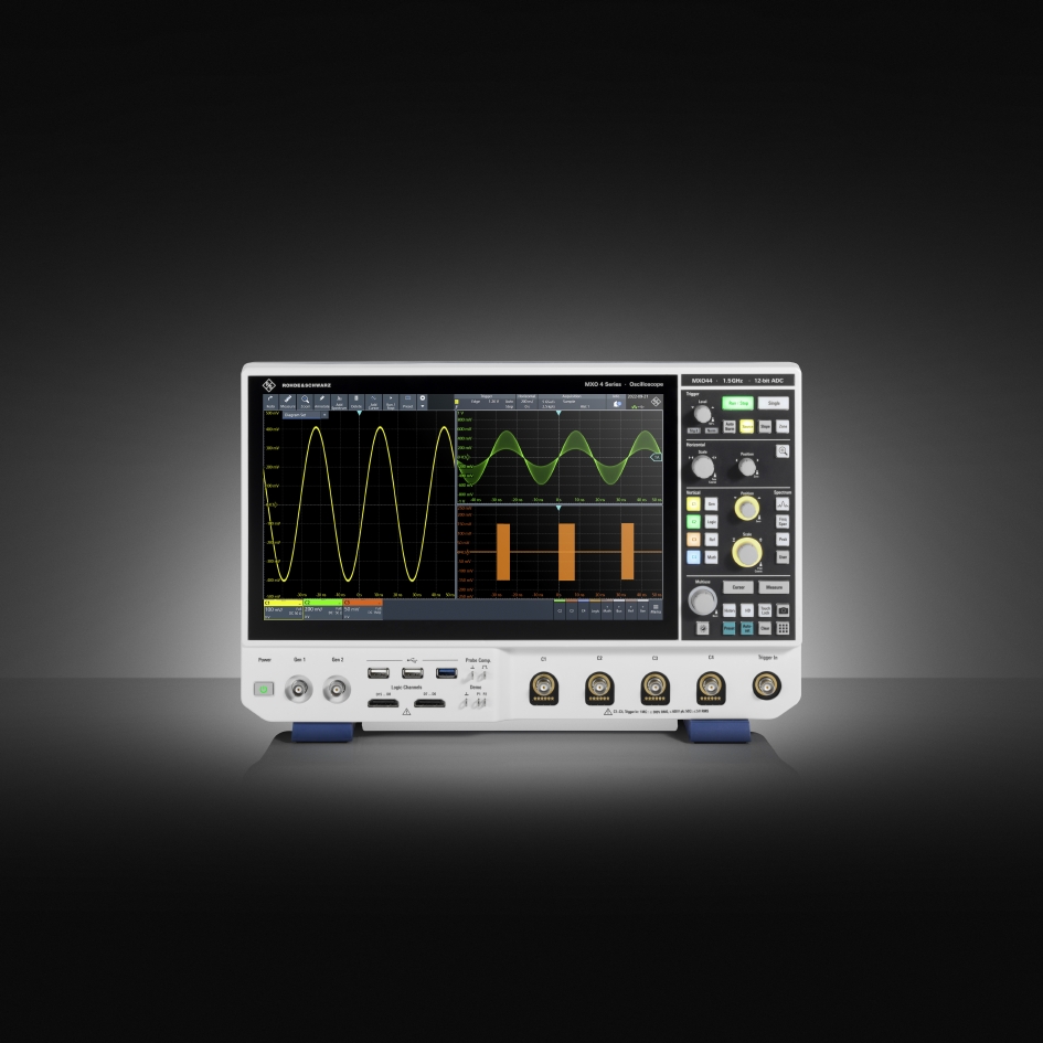
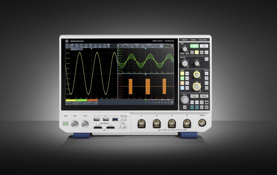
Next generation oscilloscope for accelerated insight

The Rohde & Schwarz booth spotlights the new R&S MXO 4 series, the first in a new generation of oscilloscopes. The four-channel oscilloscopes feature a brilliant 13.3” full-HD capacitive touchscreen, while delivering a number of industry firsts: The R&S MXO 4 has the fastest real-time update rate of 4.5 mil waveforms/s, letting development engineers see more signal details and infrequent events than with any other oscilloscope. The 12-bit ADC has 16 times the resolution of traditional 8-bit oscilloscopes at all sample rates. And a standard acquisition memory of 400 Mpoints on all four channels gives them 100 times the standard memory. At embedded world, visitors can experience the R&S MXO 4 first-hand in a serial protocol and decode setup, showcasing its new CAN XL trigger and decode capability.

Signal integrity test in high speed digital designs

High speed digital interfaces are at the core of electronic designs. Increasing data rates and growing integration density create new challenges for designs at the IC, board and system level. Trade show visitors can learn about powerful tools for system verification and debugging as well as compliance testing for signal integrity in interfaces, PCBs and interconnections. Demo setups at the Rohde & Schwarz booth include signal integrity interface testing featuring an advanced eye diagram, as well as high-speed digital interface compliance testing of a DDR4 design, both using the R&S RTP164B oscilloscope. A measurement of high-speed differential signal structures with accurate probe de-embedding is showcased using an R&S ZNB43 vector signal analyzer including probes and demo board.

Power electronics testing

The performance of power converters, stable and clean power rail signals, and qualified components within an embedded design are essential to reliable electronic devices. For instance, measuring the current consumption of battery-operated devices in all phases and during the transition from sleep to active modes is important for design engineers. To this end, Rohde & Schwarz demonstrates battery modelling and simulation with the R&S NGU source measure units from the R&S Essentials portfolio. Both R&S LCX200 LCR meters from Rohde & Schwarz and MFIA impedance analyzers from Zurich Instruments AG – a subsidiary since 2021 – showcase component characterization capabilities.

Detecting electromagnetic interference

Since all electronic controllers are prone to conducted or radiated electromagnetic emissions, many finished electronic products fail EMC compliance testing the first time. Every day spent debugging, isolating and correcting the EMI problem increases the time to market. As a leader in EMC testing, Rohde & Schwarz demonstrates solutions that integrate EMI testing into the product design process. Trade show visitors can learn how to use the R&S RTO6 oscilloscope as powerful tool for EMI debugging, or the R&S FPL1000 signal and spectrum analyzer for EMC pre-compliance testing.

Wireless connectivity testing

Many applications and devices such as wearables or IoT devices integrate embedded designs that feature wireless technology. The fast transition to Wi-Fi 7 supporting extreme high data rates and the advent of precise location and secure ranging applications powered by UWB, drives the demand for automated test solutions with extraordinary RF test capabilities for all phases of the product life cycle. Rohde & Schwarz will exhibit two tried-and-tested radio communication testers: The R&S CMP180 in a Wi-Fi 7 test setup showcasing IEEE 802.11be-compliant operation, and the R&S CMP200 for UWB Fira certification testing.

In-vehicle networks testing

ADAS, infotainment and 5G developments are driving up automotive data rates and have made Ethernet the de-facto technology for in-vehicle networks. However, as data rates increase, ensuring the performance and interoperability of cables and components becomes increasingly important. Testing against industry standards such as OPEN Alliance is critical for manufacturers before a product release. A multi-gigabit automotive Ethernet compliance testing setup featuring the R&S RTP oscilloscope will be on display at embedded world. Automotive customers will also find the latest Rohde & Schwarz solutions for battery testing and battery simulation, based on the company’s R&S NGM200 power supply series.

Visitors can find these and more test solutions at the Rohde & Schwarz booth 4-218 in hall 4 at the embedded world Exhibition & Conference from March 14 to 16, 2023, in Nuremberg.

For more information visit: https://www.rohde-schwarz.com/embedded-world

Exploring SparkFun NanoBeacon Board – IN100

With remarkable low power consumption features and little need for programming, the SparkFun NanoBeacon Board – IN100 and SparkFun NanoBeacon Lite Board – IN100 provide a 2.4 GHz wireless low energy beacon breakout. The IN100 NanoBeaco from InPlay is displayed on the board. The NanoBeacon Tool enables software-free module configuration, eliminating the need for complex programming to set up advertising settings for sending and receiving packets.

SparkFun NanoBeacon Lite Board


Although the design of both variants of this board is the same, there are a few small variations between them. This breakout’s Lite version, which is designed for prototyping has a reset button and power LED, is available. The reset button and power LED are not populated in the standard version, which also has male headers soldered to the board’s through-hole pins. This is because it is intended for rapid implementation and requires little assembly and customization.

IN100 NanoBeacon

An extremely low-power Bluetooth beacon module compatible with widespread 2.4 GHz protocols is the NanoBeacon IN100 SoC from InPlay.

The module can also be set up to function as a device that complies with Google Eddystone and Apple iBeacon standards. Go to the datasheet of the module for a detailed overview of the IN100.

The IN100 has the following optional peripherals:

  • Eight GPIO pins and one UART (four with multiple function options, including I2C and ADC) are present.
  • An 11-bit ADC on GPIOs that measures chip temperature and Vcc voltage.
  • For managing the power to peripheral devices, two load switches are provided.
  • One-wire sensors are compatible with the pulse count interface.

These settings enable users to wirelessly broadcast data from a variety of peripheral devices to other devices after connecting them to the NanoBeacon.

Specification:

  • Its Bluetooth low energy 5.3 is compatible with the enhanced privacy mode.
  • Beacon Modes: Private, works with Bluetooth SIG, works with iBeacon/Eddystone/Altbeacon.
  • It has 4KB SRAM, a manufacturer ID, and advertising payload storage. It also has 4KB eFuse memory.
  • On one side is a UART interface that connects to a 3.3V Serial Basic for USB communication and setting up the IN100 with the Config Tool. On the other side, four of the IN100’s GPIO pins (4–7) and the two I/O power switches are exposed (SW0 and SW1).

  • QWIC Connector: I/O pins 3 and 4 are used for SDA and SCL on the Qwiic connector on the board. In order to use this connector, I2C must be turned on for the IN100 in the Config Tool.

  • There is an RF radio with a 2.4GHz RF transmitter, support for the MedRadio band, and programmable TX output power of up to +5dBm.
  • System Power Consumption as Sub-uW power consumption for multi-year operation on a small battery and Sleep mode 650nA with 32kHz RC ON.
  • Security and privacy based on AES-128 authentication and encryption
  • NanoBeacon Boards can be powered by either a coin cell battery or the Vcc pin on the UART header.

  • The Reset button on the Lite version lets you quickly reset the board while prototyping. The Power LED is the only LED on this board. It shows that the board has power.

  • Solder Jumpers: There are three solder jumpers on the Beacon Breakout. They are labelled PWR, I2C, and BUS.

  • The operating temperature range is from -40°C to +85°C for industrial and from -40°C to +125°C for full-range industrial.
  • The NanoBeacon boards meet the Qwiic standard of 1″ x 1″ (25.4 mm x 25.4 mm) and have two holes for mounting that fit a 4-40 screw.

Applications

Standalone retail beacons, wireless sensors, asset tracking, beacon tag for RTLS (Real Time Location System), active RFID, low-power alarm system, wireless ID tag for healthcare, industrial use of wireless technology, and fitness and wellness are the common applications.

NanoBeacon Board assembled and connected to a Serial Basic.

You can find instructions in a tutorial on the Sparkfun Learn website, and the video below shows how the config tool works.


As it says in the specs, the NanoBeacon board doesn’t need to be programmed. To configure and program the IN100 in Windows, Linux, or macOS, all you have to do is use InPlay’s Nanobeacon Config Tool GUI. In a typical setup, the Sparkfun NanoBeacon board would be connected to a sensor board, like the Sparkfun BMA400 Qwiic module, and a serial board would connect the board to the host so that the config tool could be used to set up the board.

You can also download the NanoBeacon BLE Scanner app from Google Play or the Apple App Store. The company’s store sells the SparkFun NanoBeacon Board – IN100 and the SparkFun NanoBeacon Lite Board – IN100 for $5.95 each.

TOP PCB Companies