6.5W Stereo Audio Amplifier

6.5W_Stereo_Audio_Amp


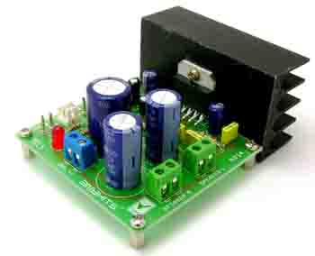
This project is a 6.5W Stereo Audio Amplifier based on TDA2004 IC.

Description

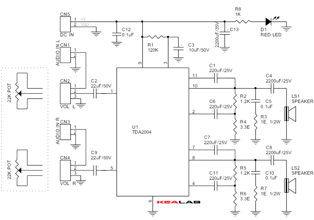
The 6.5W Stereo Audio Amplifier project built around TDA2004 IC. The TDA2004 is a class B dual audio power amplifier, specifically designed for car radio applications etc.

Specifications

  • Power supply input 15 VDC
  • Output power: 2 X 6.5 W, 4 Ohm / 2 X 10 W, 2 Ohm
  • Short circuit, thermal shut-down, load dump voltage surge protection
  • Terminal pins for connecting left and right audio signal inputs
  • Header connector for connecting potentiometer (POT) for volume adjustment
  • Screw terminal connector for easy supply input and speaker output connection
  • Power-On LED indicator
  • Heat-sink for IC
  • PCB dimensions 67 mm x 73 mm

Schematic

6.5W_Stereo_Audio_Amp_SCH


Parts

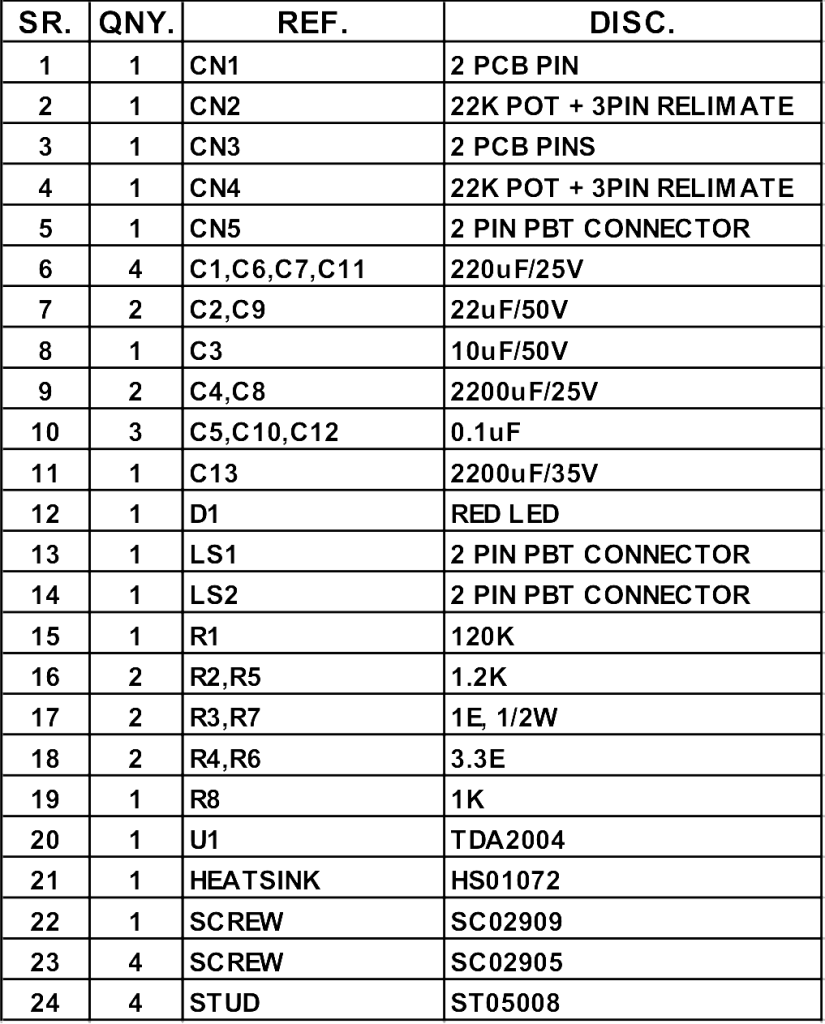
6.5W_Stereo_Audio_Amp_BOM

Mini Stereo Audio Amplifier

Mini_Stereo_Audio_Amplifier


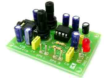
This project is a Mini Stereo Audio Amplifier based on TDA2822 IC.

Description

The dual low power amplifier built around TDA2822 8pin DIP. IC, it is mainly designed to use in portable players, radios and other building block project. A 3V supply can be used to drive headphones providing 20mW in 32 Ohms per channel, and a 12V power supply will provide 1W in 8 Ohm per channel for small loudspeakers.

Specifications

  • Supply 9V DC (supply Range 3V to 12V)
  • Load 8 Ohm Speaker
  • Gain 39dB
  • Input Impedance 100K Ohm
  • THD 10%
  • Frequency Response 20Hz to 20Khz

Schematic

Mini_Stereo_Audio_Amplifier_SCH

Parts

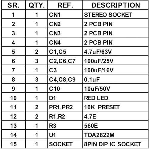
Mini_Stereo_Audio_Amplifier_BOM

Digital Stopwatch 0-60sec

schem60

Introduction

By using the same circuit of the Digital Stopwatch 0-99sec , we can add an AND gate, and transform the 0 – 99sec stopwatch to a 0 – 60sec stopwatch.

We must find a way to control the RESET function of the BCD counter, which is responsible for the counting of the seconds. As we studied above, the circuit resets when we have 99 to 100, that is 1001 1001 à 0001 0000 0000. To make a transformation successfully we must force the pulse from 59 to 60 0011 1001 à 0100 0000 on the output of the BCD counter.

By placing the AND gate, with its inputs on the Q1 and Q2 of the BCD counter of the decades, we make sure that when the gate closes, the RST input of the BCD counter will be set to logical “1”, which on its turn, will force the circuit to start over. The transformed circuit appears in the above picture.

Digital Stopwatch 0-99sec using digital ICs

schem99

Introduction

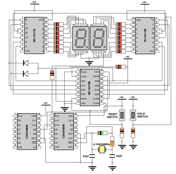
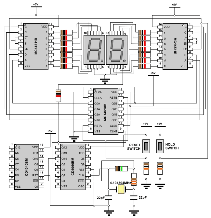
In the present article, we will describe the function of a digital stopwatch, 0 – 99 sec. The function of the stopwatch, relies in the use of 4 integrated circuits. It is obvious that other integrated circuits can be used to achieve the same result, however in this case we have used the following parts:

  • 1 x CD4060BM (14 stage ripple carry binary counter)
  • 1 x CD4040BM (14 stage ripple carry binary counter)
  • 1 x MC14518B (BCD counter)
  • 2 x MC14511B (BCD to seven segment driver)
  • 2 x 7 segment LED displays

The circuit that has been used is shown in picture 1. Through the experimental part we will explain each of the parts function, but in order to have a notion of the basic idea, let just say, that this circuit besides the 5V power supply, is fed with a pulse which comes from a crystal. The crystal’s pulse is devided properly in order to obtain the 1 Hz pulse which we need in order for the circuit to work properly, and display the seconds on the 7 segment displays, through a procedure which we will explain through the experimental part.

Description

We will begin the description of the digital circuit above. For our convenience we will devide the circuit to 2 parts: the generator, which produces the pulse of the desired frequency, and the part that does the actual counting.

Generator

The generator of the circuit comprises of the integrated circuits CD4040CM and CD4060CM. We use a crystal which oscillates at a frequency of 4,194,304MHz. It is obvious that this frequency is completely useless, as it is too big to be used as it is to our circuit. What we should is devide this frequency, in a way that in its final form, the pulse will have a frequency of 1Hz, which is the desirable frequency. Initially we use the integrated CD4060, which devides the imported frequency in its input, by forces of 2. As we can see on the integrated circuit the outputs are marked as Q4, Q5,… Qn. By importing a pulse in the CLK input of the 4060, with a frequency f Hz, we take out of output Qn, a signal which has a frequency equal to f/2n,. So, by exporting the signal out of Q14, knowing that the imported signal has a frequency of 4,194,304Hz, we take a signal, which has a frequency of 256Hz.

By importing this signal, to 4040 and by exporting the signal through Q8 we have finally taken an inverted signal, at the frequency of 1Hz. The fact that the signal is inverted, firstly doesn’t affect the proper function of our circuit and secondly is due to the inversion of the CLK input as we can see. This inversion just causes, the following circuit to be triggered with a logical “0”. By putting a LED on the same output, we have a visual of the counting, as in each positive pulse the diode polarizes positively, and a current passes through it.

Counter

The signal of 1Hz, which we have taken from the generator, is imported to a BCD counter MC14518. This integrated circuit adds a logical “1” at each pulse, on its output.του. .The MC14518 is virtually divided into two segment. One counts the units of the seconds, while the other the decades. As we can see in picture 1, the generators pulse is imported to the part which counts the units. This is very logical, as we want in each secont the number of the display to be raised by 1. On the other hand, we want the first display to raise by 1, every 10 seconds. This is why, we ground the CLK input, and we use the signal of Q3 to the CKE input.

By using this means, we make sure that the first display will be triggered, only when we have a decreasing signal on Q3; that is, only when the signal drops from logical “1” to logical “0”. As we can see, the first display increments every 10 seconds, which means that after 9 on the second display (1001 on the output of the BCD counter) the first display must be set to zero, while the first must be set to +1. That is that from 1001 à 0000, and we have a descending pulse, as the last digit descends from logical “1” to logical “0” and triggers the BCD counter of the decades. When the decades display becomes 9 then the circuit goes to the next state, which is zero, and the counting begins once more.

The integrated circuits MC14511 are BCD to 7 segment drivers. As its name clearly state, their sole purpose is to translate the BCD information of MC14518, to a code understandable by the 7 segment displays. The inputs image002 (Lamp Test, Blanking) are used to test the LEDs of the display and pulse modulate the brightness of the display. In this case we these inputs to logical “0”, as we don’t need them. The LE input (Latch Enable) is used to keep the number of the displays while the pulse still runs. It is a HOLD function similar to the one of the modern stopwatches.

In addition, at any given moment we can restart the counting, by pressing the reset switch. By this means we set the RST input of the MC14518 to logical “1”, which resets the counting to 0000.
2 Channel Relay Board

2_Channel_Relay_Board_PIC

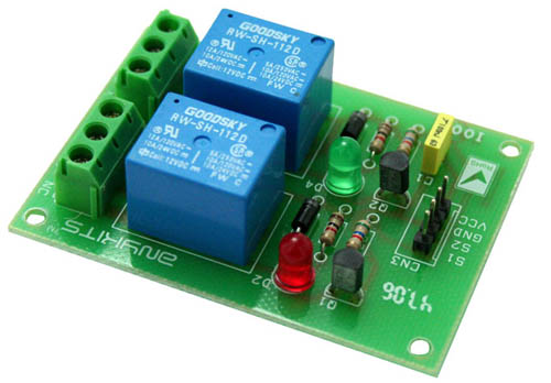
This project is a 2 Channel Relay Board.

Description

2 channel Relay driver project can be controlled by feeding 2-12V trigger voltage, Very useful project for application like Micro-Controller based projects, Remote controller, Lamp on Off, and any circuits which required isolated high current and high voltage switching by applying any TTL or CMOS level voltage. Two LED works as operation indicator while in , 3 pins screw terminals to connect load and provides  both normally open and normally closed switching.

  • Input: 12 VDC @ 84 mA
  • Output: Two SPDT relay
  • Relay specification: 5 A @ 230 VAC
  • Trigger level : 2 to 12 VDC
  • Header connector for connecting power and trigger voltage
  • LED on each channel indicates relay status
  • Power Battery Terminal (PBT) for easy relay output connection
  • Four mounting holes of 3.2 mm each
  • PCB dimensions 49 mm x 68 mm

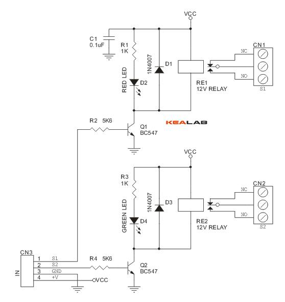
Schematic

2_Channel_Relay_Board_SCHEMATIC

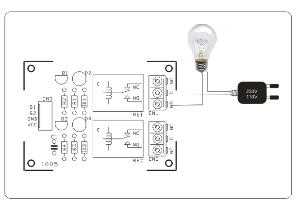
Connection

2_Channel_Relay_Board_CONNECTIONS

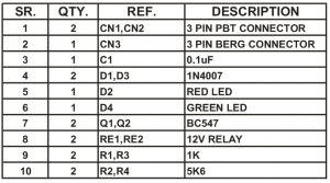
Parts List

2_Channel_Relay_Board_BOM

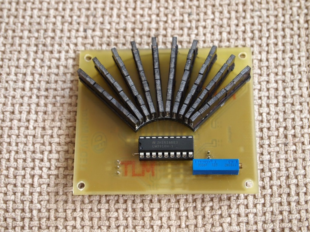
LED VU Meter with LM3916

LED_VU_Meter_(3)

This project is a LED VU meter based on LM3916.

Description

LM3916 is a dedicated IC for VU LED meter. Unlike LM3915 which have 3dB step between voltage levels, the LM3916 have nonlinear steps: -20, -10, -7, -5, -3, -1, 0, +1, +2, +3db, just like old school analog VU meters. I saw in YouTube an interesting commercial LED VU meter, which imitates the needle movement in analog VU meters and I thought I can make a similar one. All I needed I found in the datasheet of LM3916.

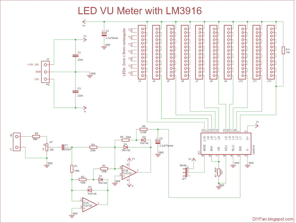
 The LM3916 can be feed with AC signal without any rectification, but I wanted to implement a precision full wave rectification. I chose the schematic on page 13, fig.21 of the datasheet: “Precision Full-Wave Peak Detector”.

The LEDs are connected via sockets J3 to J12 (only one row LEDs is shown on the schematic) and I found that it’s cheaper to use a 28 pin IC sockets cut in half than regular 40 pin sockets. Of course LEDs can be soldered directly on the PCB.

The schematic needs bipolar power supply to work correctly, but the negative rail can be as low as -5V or even -3.3V. The positive rail must be bellow +25V and combined voltage of negative and positive rails must not exceed 36V. The minimum positive rail voltage depends on the voltage of the LEDs. For example if the LED have 1.9V forward voltage and we have 7 LEDs on one pin, then the minimum positive voltage will be 7*1.9V + 1.5V (drop voltage at LM3916) = 14.8V. The green LEDs usually have little higher forward voltage – 2.2V – 2.4V, so +18V will be sufficient in most cases.

The LEDs current is determined by R1_REF, and with 2.2k resistance it will be 5 – 6 mA.
The formula is Iled = 10 * (1.2V / R1_REF).

IC2 is connected as precision full wave rectifier and can be any general purpose dual opamp – TL072, TL082, LF353.

The output mode can be set with 3-pin jumper JP1. Shorting pins 1-2 will set the bar mode and shorting pins 2-3 will set the dot mode.

The max input voltage of the LM3916 is set to 1.2V, and with R8-R7 we can adjust the input level.

The color of the LEDs is your choice. I used green LEDs for negative levels, yellow for 0dB and red for positive levels. For this project I bought transparent rectangular LEDs, but they have two drawbacks. First – when one column lights up the adjacent columns also significantly lights up. My solution was to paint the sides of the LEDs with black marker. There also can be used a black tape around the entire collumn.

Second drawback is that because of the transparency, the LEDs emit light from one point, which is not very pleasant. The solution here was to rasp the top side of the LEDs with rough file, so the light to diffuse more even.

Schematic

LED_VU_Meter_(schematic)

RGB LED Disco Lights

RGB_LED_Based_Disco_Lights_th

This project is a microcontroller based RGB LED lights effects.

Description

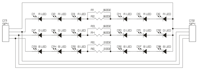
RGB LED disco light is a simple project designed around PIC16F72 microcontroller.

This firmware is a RGB driver, as name suggests it is used to derive or light red, green and blue LEDs in particular fashion. Its main feature is the pattern shown on LEDs. It is quite difficult to describe pattern in words but we want to specify that first it will derive red then green then blue three times and then a particular pattern is shown on LEDs and again the three LEDs light.

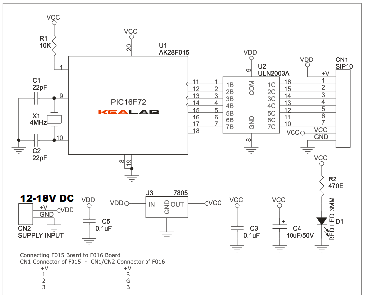
In this project we have used PIC 16F72 microcontroller. The various pin configurations are shown below:

  • OUTPUT: PORTC
  • Red Led: PORTC.F0
  • Green Led: PORTC.F1
  • Blue Led: PORTC.F2
  • External Oscillator (crystal: 4MHz)
  • Microcontroller: PIC 16F72
  • SUPPLY : 12-18V DC

Schematic

RGB_LED_Based_Disco_Lights_main_board_schematic

RGB_LED_Based_Disco_Lights_LED_Board_Schematic_th

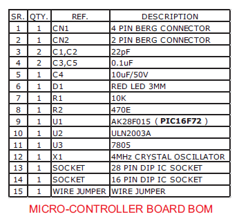
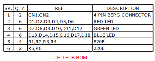
Parts List

RGB_LED_Based_Disco_Lights_main_board_BOM

RGB_LED_Based_Disco_Lights_led_board_BOM

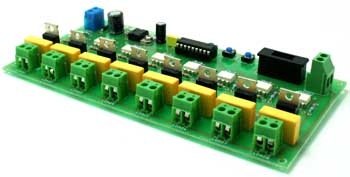
Microcontroller based running light controller

picture

This project is a lights effects board using common bulbs.

Description

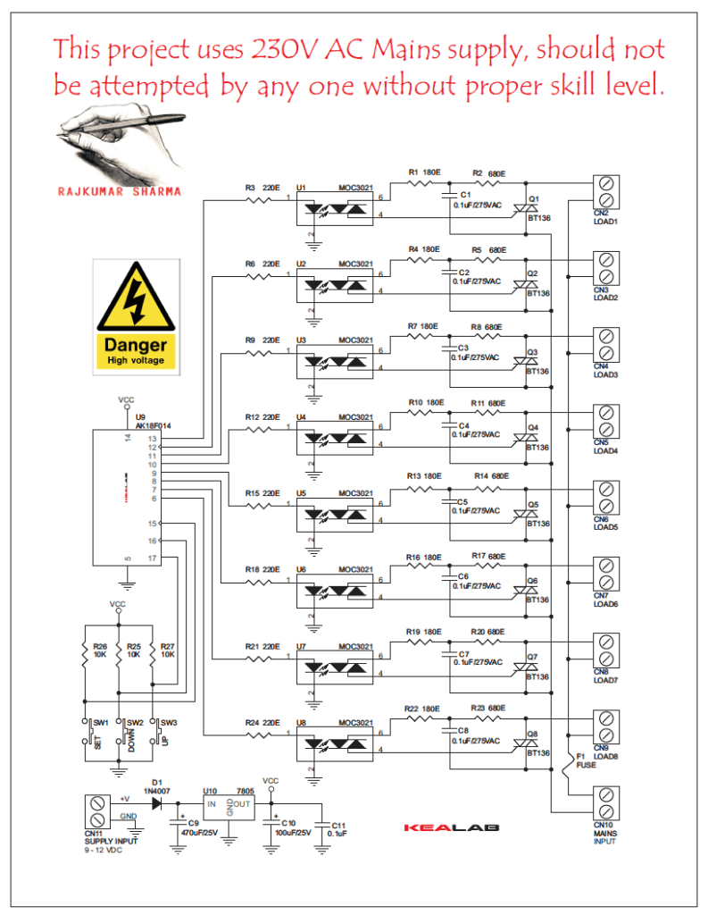
This project provides some lighting effect by the blinking pattern of the bulbs connected at its output. Up to 8 Bulbs can be connected in between connector CN2 to CN9 and AC power to control them should be connected at Connector CN10. DC Power should be applied at Connector CN11 in accordance with the polarity marked on this connector. Care should be taken while using this it as it contains Main Power on the board.
We can change the Blink pattern by the press of the SET switch and change the blinking speed by the press of the UP and DOWN keys on the PCB. Fuse F1 will protect the Kit from any possible short circuit and excess current flowing through it.

Features:

  • Microcontroller based design for greater flexibility and ease of control
  • Triac based switching of loads connected to the circuit
  • Industry standard isolation with the help of Opto enabled Triac Control
  • Fuse protection for AC output
  • SUPPLY 9-12V DC & 230V AC
  • LOAD-100W max on each output
  • Simple and easy to use 3 tactile switch enabled control of the project
  • PBT type connector for connecting supply (AC/DC) and TRIAC output on the PCB
  • Onboard regulator for regulated supply to the project
  • Diode protection for reverse polarity connection of DC supply to the PCB
  • Four mounting holes of 3.2 mm each
  • PCB dimensions 86 mm x 173 mm

Schematic

schematic

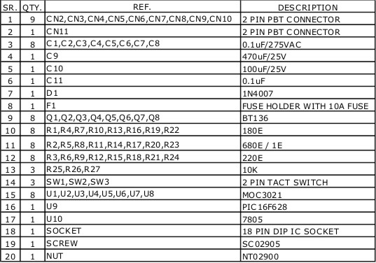
Parts List

BOM

Triac based lamp dimmer

F001

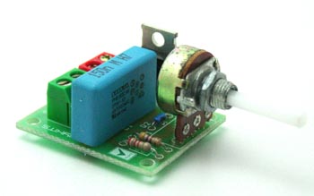
Triac based Indecent lamp dimmer is a simple circuit and it doesn’’t requires additional power supply, works directly with 110V AC or 230V AC.

Description

It is a low cost dimmer circuit for adjusting the light brightness of incandescent, Halogen Lamp, Light Bulb load up to 250 W.

Features:

– Input supply: 230 VAC or 110 VAC
– Output: 250 W
– Triac controlled
– On board Potentiometer for adjusting level
– Power Battery Terminal (PBT) for easy input / output connection
– Four mounting holes of 3.2 mm each
– PCB dimensions 40 mm x 34 mm

Schematic

SCH

Circuit description

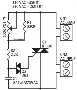
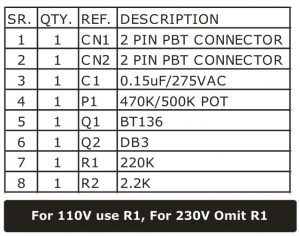
This kit consists of BT 136 Triac, resistors and capacitor.  CN1 connector is for Load connections and CN2 connector for power supply connections.

BT136: It is a sensitive gate Triac, used in general purpose bidirectional switching and phase control applications where high sensitivity is required.

DB3: It is a DIAC that functions as a trigger diode with a fixed voltage reference.  It can be used in conjunction with Triac for simplified gate control circuits or as a starting element in fluorescent lamp ballasts.

Working principle

This kit is used as a Light dimmer kit.  It is used to adjust the brightness of the Halogen Lamp, Light Bulb up to 250 W.  A power supply of 230 or 110 VAC is supplied to the kit at CN 2 connector and a light bulb is connected at the CN 1 connector.  Using the POT we can adjust the brightness of the bulb.

Applications

It is used to adjust the brightness of incandescent, halogen lamp, light bulb up to 250 W.

Parts List

BOM


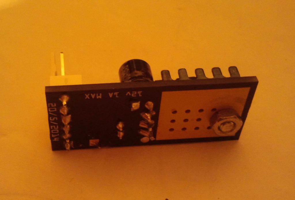
Temperature Controlled PC FAN

photo_1

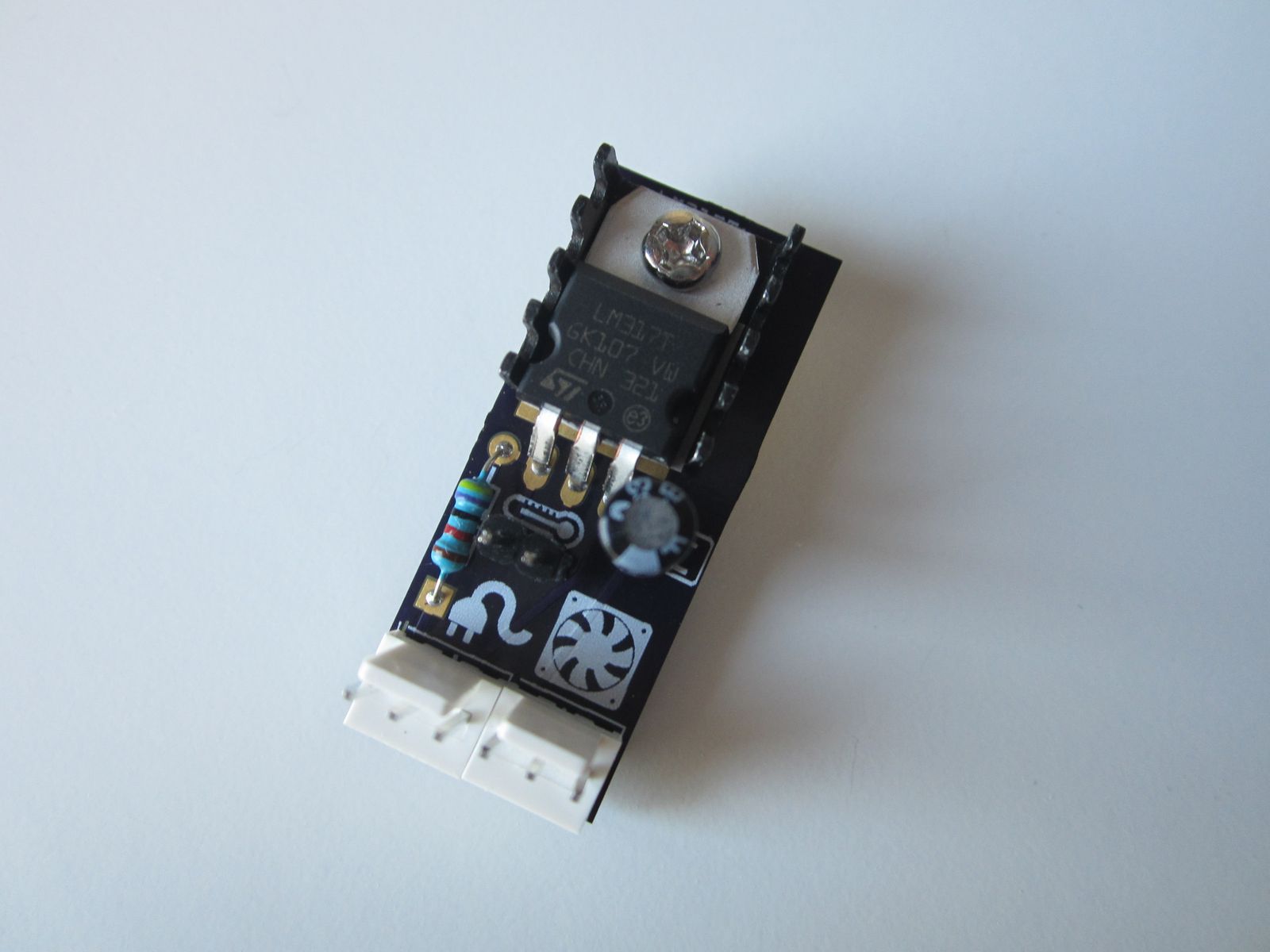
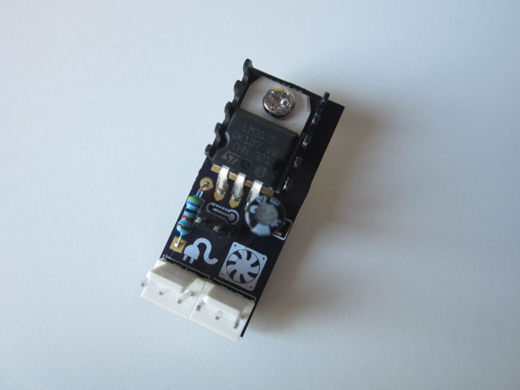
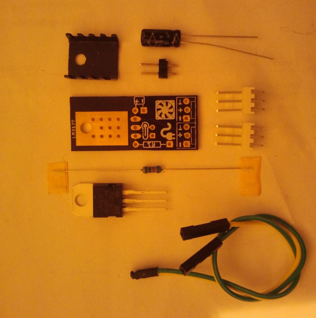
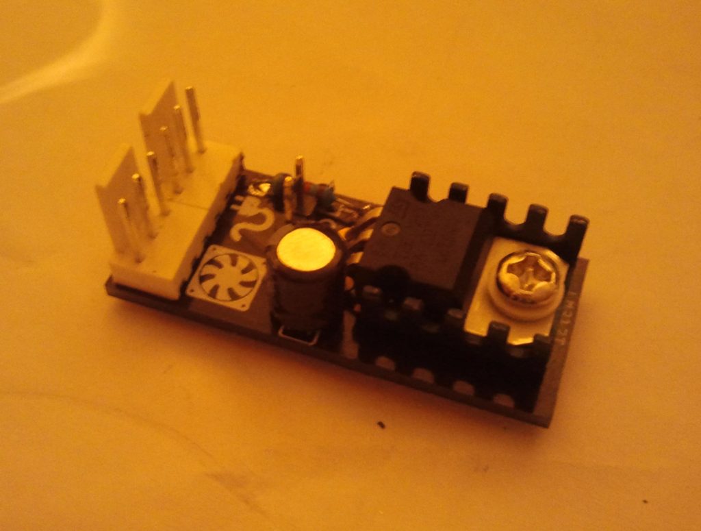
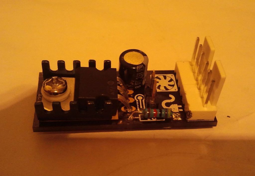
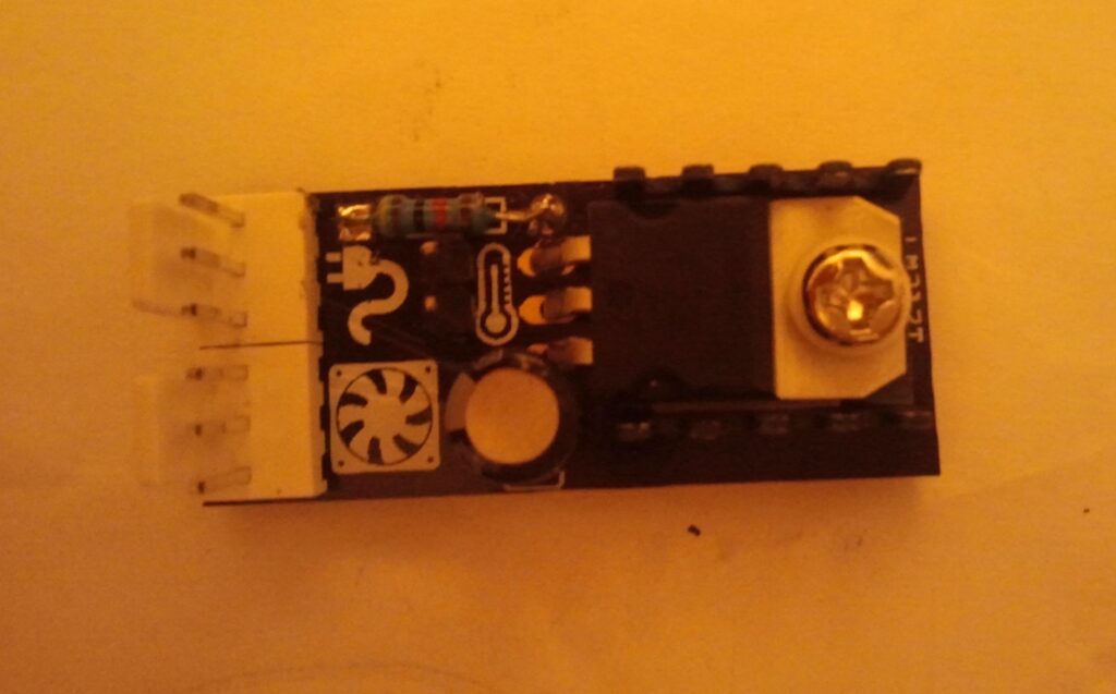
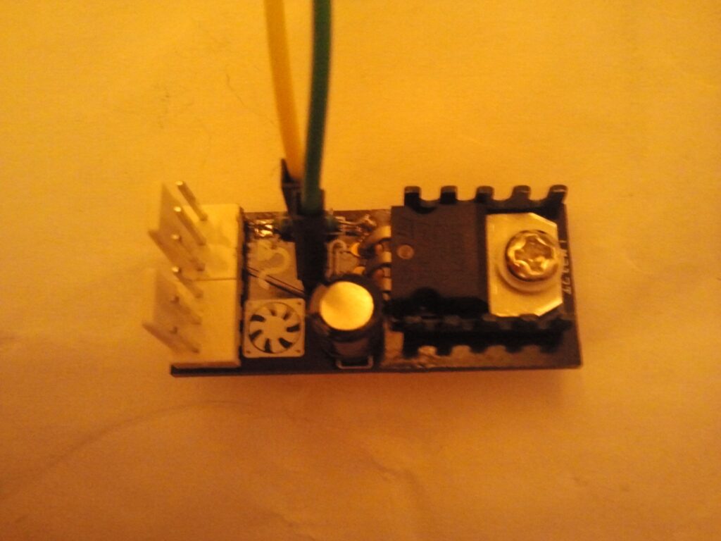
This project is a temperature controller for a PC FAN. It regulates the speed of the FAN attached to it according to the measured temperature. Temperature is sensed using a simple NTC thermistor.

Description

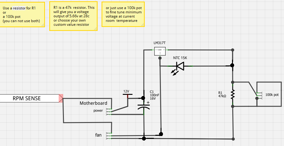
In most PCs, the fan runs constantly, which may not be necessary. A simple circuit can regulate the fan speed according to temperature. This not only saves energy, but it also reduces fan noise. Only three components are needed to allow the fan speed to be controlled according to the actual temperature: one adjustable voltage regulator (LM317T) and two resistors that form a voltage divider. One of the resistors is an NTC thermistor (temperature-sensitive resistor), while the other is a normal resistor.

schematic

Components list

  • 1 x LM317T
  • 1 x 100K POTENTIOMETER 3296W 3296
  • 1 x 15K NTC
  • 1 x 100UF 16V Capacitor
  • 1 x TO-220 HEATSINK (OPTIONAL)
  • 2 x Latching Pin Headers 0.1″ Pitch 3 Way

This PCB has been designed so you can use a single resistor or a 100k potentiometer, i recommend using the 100k pot as this is far much easier to fine-tune this device for your needs.

Photos

SAMSUNG

SAMSUNG

SAMSUNG

SAMSUNG

SAMSUNG

SAMSUNG

TOP PCB Companies