6V Ultra-Bright LED Chaser

6V_Ultra_Bright_Chaser_pic2

General

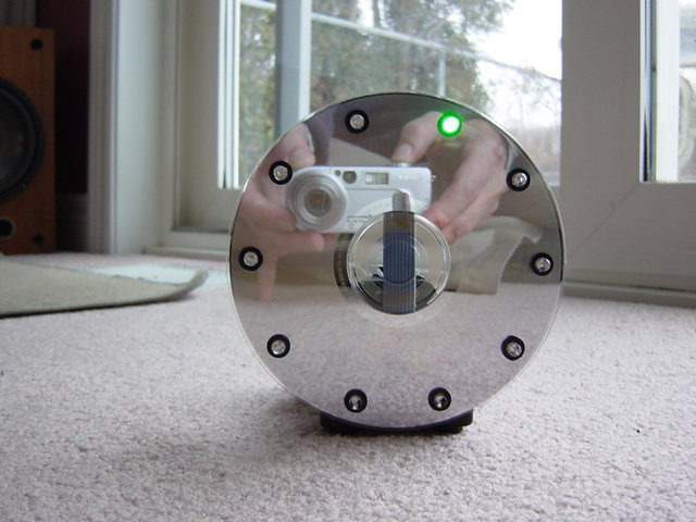
This is a spectacular but completely useless project. It lights Ultra-Bright LEDs in a sequence and each LED flashes brightly very briefly. The LEDs light-up going around and around since they are mounted in a circle (on a CD), then they pause before chasing again. The very brief flash of each LED (15ms) and the pauses (1 second) reduce the average current so the battery should last a long time.

For user convenience, this project has a stepper speed control and a brightness control. At slower speeds and/or reduced brightness, the battery’s life is extended considerably.

At full brightness, the LEDs flash extremely brightly. More than one of this project grouped together occasionally synchronize, lighting the whole room for a moment.

Operation

At maximum speed, the LEDs don’t appear to flash, instead they appear to move from one lighted one to the next, around and around. They rotate completely for 4 rotations in two seconds, and then turn off for a one second pause then repeat the sequence. At a lower speed, the number of rotations before the pause is less. It will do three rotations, two or even only one rotation at its slowest speed. A sequence of rotations starts with LED #2 and end with LED #9.

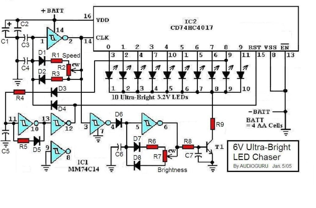
6V_LED_Chaser_schematic

Specifications

Battery: Four AA alkaline cells.
Battery life:

  • Minimum speed and brightness                 2.3 years
  • Medium speed and brightness                    1 year
  • Minimum speed, maximum brightness   4.1 months
  • Maximum speed and brightness                3.8 weeks

Brightness: controlled with Pulse width Modulation, from off to extremely bright (4000mcd).
Stepper speed: 2 LEDs/sec to 2 revolutions/sec.

Pulse Width Modulation frequency: 3.9KHz.
LED current: 24mA pulses.
LED voltage drop: 3.2V at 24mA. Blue, green and white Ultra-Bright LEDs are suitable.
Minimum battery voltage:

  • <3V, oscillators do not run.
  • 3V, LEDs are very dim.
  • 4V, LEDs reach almost full brightness.

Radio interference: none.

Circuit Description

  • The CD74HC4017N high-speed Cmos IC is rated for a maximum supply voltage of 7V. It is rated for a maximum continuous output current of 25mA. In this project, the maximum supply voltage is 6.4V with brand new battery cells and the 24mA output current is so brief that the IC runs cool.
  • The MC14584BCP* IC (Motorola) is an ordinary “4XXX series” 3V to 18V Cmos IC, with a very low operating current and low output current. Its extremely high input resistance allows this project to use high value resistors for its timers and oscillators, for low supply current. Its 6 inverters are Schmitt triggers for simple oscillators and very quick switching.
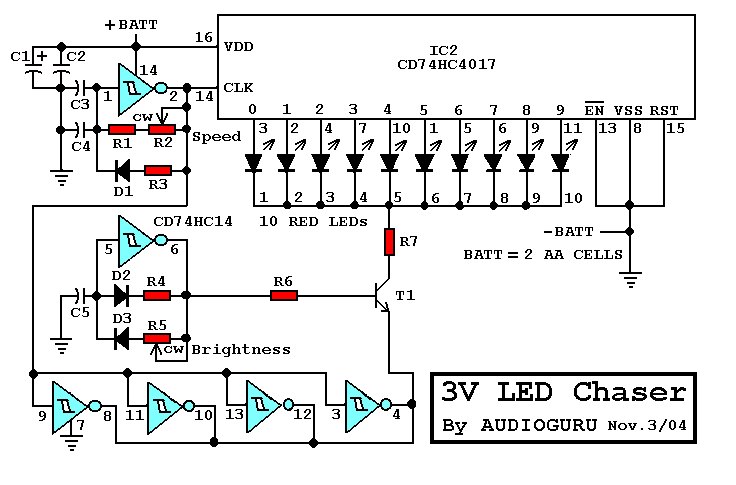
  • IC2 is a 10 stage Johnson counter/decoder. On the rising edge of each clock pulse its outputs step one-at-a-time in sequence. It drives the anode of each conducting LED toward the positive supply.
  • IC1 pins 1 and 2 is a Schmitt trigger oscillator with C3 and C4 paralleled for a very low frequency. R1 and R2 control its frequency and the diodes with R3 combine with the capacitors to produce the 15mS on time for the LEDs.
  • IC1 pins 5 and 6 is the brightness Pulse Width Modulation oscillator. The pot R7 with the associated diodes and resistors allow it to change the duty-cycle of its output for PWM brightness control. It drives the transistor.
  • IC1 pins 3 and 4 is an inverter. It takes the low time (LEDs off) from the clock oscillator, inverts it to a high and shuts-off the brightness oscillator through diode D6.
  • IC1 pins 11 and 10 is a sample-and-hold stage. It takes a sample of the pulse driving LED #9 though D3 and R4 and charges C5 in steps. At maximum speed it takes 4 steps for C5 to charge to the Schmitt switching threshold voltage. R5 and D5 slowly discharge C5 for the pause time.
  • IC1 pins 13 and 12 is an inverter that resets the counter/decoder and shuts-off the clock oscillator through D4, during the pause time.
  • IC1 pins 9 and 8 is not used and is shut-off by grounding its input.
  • T1 is the PWM switching transistor. R9 limits the maximum LED current to 24mA.

Construction

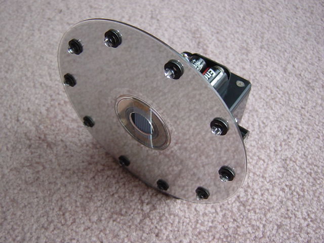
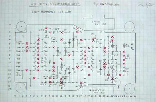
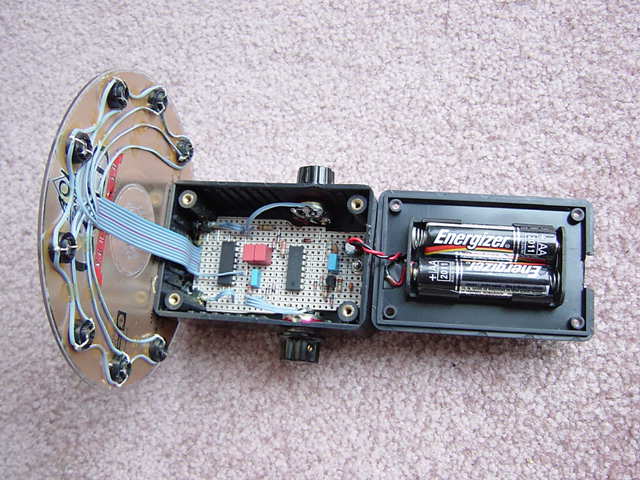
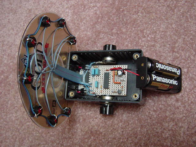
The 10 LEDs mount on a Compact-Disc which is glued to a plastic box with contact cement. The box houses the Veroboard circuit in its lower main part with the battery holders on its lid. Multiconductor ribbon cable joins the LEDs to the circuit. The pots mount on the sides of the box.

If you turn it down each night, its current is so low an on-off switch isn’t needed.

6V_Ultra_Bright_Chaser_Veroboard_layout

Parts List

1 IC1 MC14584BCP (Motorola) * Ordinary Cmos hex Schmitt trigger inverters
1 IC2 CD74HC4017N High-speed Cmos decade counter/decoder
1 T1 2N3904 or 2N4401 NPN transistor
8 D1 to D8 1N4148 or 1N914 Diodes
10 LEDs Blue, green or white Ultra-Bright LEDs with Vf = 3.2V or less at 20mA
1 R1 100K 1/4W resistor
1 R2 1M Linear-taper potentiometer
1 R3 33K 1/4W resistor
1 R4 2.2M 1/4W resistor
1 R5 22M 1/4W resistor
1 R6 47K 1/4W resistor
1 R7 1M Audio-taper (logarithmic) potentiometer
1 R8 1.8K 1/4W resistor
1 R9 68 ohms 1/4W resistor

1 C1 100uF/16V Electrolytic capacitor
1 C2 0.1uF/50V Ceramic capacitor
2 C4 and C4 1uF/63V Metalized poly capacitor
1 C5 470nF Metalized poly capacitor
2 C6 and C7 1nF Metalized poly capacitor

* A CD74C14 can also be used for IC1 but R4 = 1M, R5 = 10M, C3 and C5 = 330nF, C4 = 470nF.

A 3V LED Chaser project also works well with these changed parts but using a CD74HC14N for IC1.
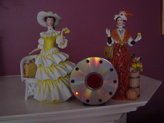
In addition to these changes, R8 = 680 ohms and R9 = 22 ohms. I built one using low-voltage (1.8V at 20mA) orange Ultra-Bright LEDs. The orange one looks good beside the green one.

Attachments: 6V LED Ultra-Bright Chaser schematic, Veroboard layout and 3 pictures.

I wish I knew how to take a slow picture with my son’s digital camera, so all the LEDs would be lighted, and if I moved it would make nice lighted smears in the picture.

Photos

6V_Ultra_Bright_Chaser_pic1

6V_Ultra_Bright_Chaser_pic3

High Power LED mood Lamp

image_1

Introduction

In this page we will introduce a great project designed by Toon Beerten. His project named “DIY Led Mood Lamp” can become a very interesting add-on for your room that’s absolutely sure it will impress everyone. As you can see on the photos, we talk about a color fading lamp, that looks amazing!

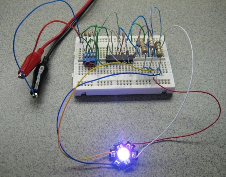
The purpose of this page is to try to give some hints building it successful. This high power led mood light is based on PIC16F628 and the ability of this mcu to produce PWM pulses. Varying pulse width we can produce millions of color combinations using only the three basic colors. So only one RGB (Red-Green-Blue) led is capable producing a rainbow of fading colors.

image_4

With the help of four switches we can handle all functions of the lamp. We can choose fading or jumping between colors, we can select a rainbow style or a random color changing behavior, we can choose slow or fast changing of colors and we can pause on a desired color.

Finally we will make some power dissipation measurements to help us select an appropriate power supply unit.

Housing

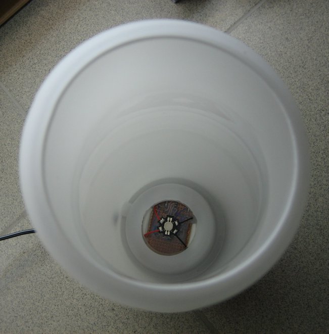
You can use your imagination to find a housing that will be able to diffuse colors uniformly. Color difussion is necessary to achieve best results. In original design the author used the 45cm IKEA Mylonit lamp. That’s a great housing for your lamp. Instead you can use the smaller 31cm IKEA Mylonit lamp with the same amazing results. That’s the lamp we used in our construction.
image_2

In our research we found other lamps (ex. sphere shape) that are ideal for housing your big led.

High Power LED

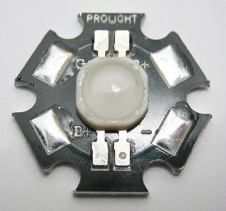
Minus on the bottom right pin is common anode (positive voltage) – it’s manufactured wrong

The led used is a high power 3W RGB LED. It can be found on ebay at LEDSEE-electronics. You can also check ebay for other high power RGB leds. It will do the jod the same way. Details of this brilliant led shown below.

3W high power RGB LED

Light Angle of the LED 140 degree°
Nominal current B,G,R 350mA
Forward voltage:
Red Typ 2,2V
Green Typ 3,55V
Blue Typ 3,55V

Wavelength of the LEDs:
Red Typ 625nm
Green Typ 530nm
Blue Typ 470nm

Luminous Intensity:
RED Typ 32lm
Green Typ 35lm
Blue Typ 10lm

LED type: Common Anode

Schematic

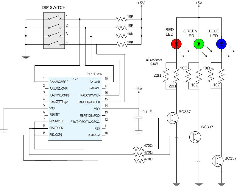
The schematic used is shown in the next image. It’s as simple as it shows. Take care on the correct transistor mount and correct polarity of power source.

Schematic

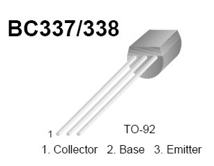
BC337 Pin out
BC337 Pin out

Parts List

Here is a list of the components i used for making the led mood lamp.

  • 3 x NPN transistors capable of driving 500 mA, for example the BC337
  • one PIC 16F628(A) and a programmer
  • a small perforated circuit board
  • 7 x 10K resistors (1/4W)
  • 1/2 watt resistors (2x 22 Ohm, 4x 10 Ohm) and a DIP switch
  • a power supply (5 volts, 500 mA)
  • Ikea Mylonit lamp or other housing
  • silicon paste from your local DIY shop (if you want to use a heatsink)
  • one z-power 3 watt rgb led
  • a little heatsink and some cooling paste (if you want to use a heatsink)

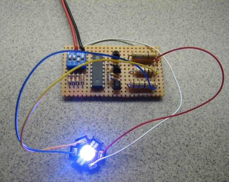
Circuit board

On the next image you can see the circuit arranged on a perforated board.

image_5

Programming The PIC 16F628 Microprocessor

Programming the PIC16F628 can be achieved using this very simple pic programmer and a program called ic-prog. Just use your programmer and upload the .hex file on your PIC. For successful results you should pay attention on the fuse bits. You should enter the correct fuses as noted on the following table.

Fuses

IntRC I/O = Enabled
PWRT = Enabled
BODEN = Enabled
MCLR = Disabled
Rest of fuses = Disabled

DIP Switches functions

SW1 – makes you choose between G->GB->B->BR->R->RG–>>G effect and random color change effect
SW2 – makes you choose between fading and jumping from one color to another
SW3 – makes you choose between slow or fast
SW4 – pauses at the current color displayed

Mounting

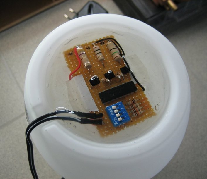
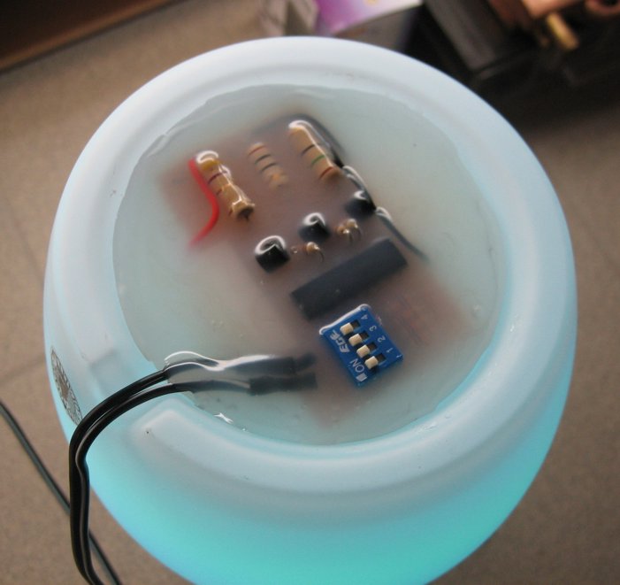
A good way to mount the circuit board is to use a hot glue gun to “mold” the circuit underneath the lamp housing. There is plenty of space there for your board. At the next photos you can see the circuit board mounted on the small 31cm IKEA Mylonit Lamp.

The glue is still hot. Temperature of glue didn't damage the PIC or other parts.
The glue is still hot. Temperature of glue didn’t damage the PIC or other parts.
The glue is now cold and you can easily access the dip switches. Lamp is working!

image_8

Update – 10/2009

Steve Rougier made improvements on the original code and schematic adding additional operation modes. For detailed info and for updated source code check on this zip file: rougier

3V LED Chaser

3V_Chaser_3

General

There are many 9V chaser circuits that seem to waste about 7V when driving LEDs that are only about 2V. This project is unique, because it uses only two inexpensive alkaline battery cells totaling 3V for power. Since most of the waste is eliminated, the cells last a long time.

Unlike the other circuits, this one flashes the LEDs for only about 30ms each, further extending the battery life. For user convenience, it has a stepper speed control and a brightness control. At slower speeds and with reduced brightness, the battery life is further extended considerably. Mounted in a circle, the LEDs appear to rotate as they step from one to the next.

3V_Chaser_1

Specifications

  • Battery: Two alkaline cells (AA size were used in the prototype)
  • Battery Life: AA cells C cells D cells
  • Minimum speed and brightness 8 months 2 years 4.9 years
  • Medium speed and brightness 6 months 1.5 years 3.6 years
  • Maximum speed and brightness 2 weeks 1.5 months 3.6 months
  • Stepper speed: 2 LEDs/sec to 2 revolutions/sec
  • Brightness: Controlled with Pulse Width Modulation, from very dim to 161mcd (very bright)
  • Pulse Width Modulation frequency: 1.4KHz very bright to 6KHz very dim
  • LED current: 15mA pulses, reduced to 10.5mA at maximum Pulse Width Modulation
  • LED voltage drop: 1.76V (measured, not rated) @ 10.5mA
  • Minimum battery voltage (total of both cells): <1.24V, circuit is running but LEDs are not light
  • 1.6V, LEDs are very dim at maximum brightness
  • 2.0V, LEDs reach almost full brightness, battery replacement is recommended.
  • Radio interference: None

Circuit Description

The 74HC Cmos ICs are rated for a 2V to 6V power supply for high-speed logic circuits. They continue to operate at a much lower voltage but no longer meet high-speed logic specifications. To reach high speeds, their output current can momentarily exceed 400mA (low voltage drop) but thermal considerations limit maximum continuous output current to 20mA. Perfect for driving LEDs!

•IC2 is a 10 stage Johnson counter/decoder. On the rising edge of each clock pulse its outputs step one-at-a-time. It drives the anode of each conducting LED toward the positive supply.
•IC1a is a standard Cmos inverter Schmitt-trigger oscillator with C3 and C4 totaling 800nF for a very slow step rate. R2 is the speed control pot with R1 limiting its maximum speed. It clocks IC2 and feeds the inverters/drivers. D1 and R3 reduce its output high time to 30mS.
•IC1d, IC1e, IC1f and IC1b are paralleled inverter/drivers for a low output voltage drop and drive the emitter of T1 to ground.
•IC1c is another standard Cmos inverter Schmitt-trigger oscillator. R5 is its Pulse Width Modulation control and with D3 performs dimming of the LEDs. D2 and R4 extend the PWM’s maximum pulse width.
•T1 is a transistor that is used as a PWM switch. R7 limits maximum LED pulse current.
•C1 bypasses the battery’s supply voltage at low frequencies and C2 bypasses at high frequencies.

Construction

The ten LEDs mount on a Compact-Disc which is glued to a plastic box with contact cement. The box houses the Veroboard circuit in its lower main part with the battery holder in its lid. Multiconductor ribbon cable joins the LEDs to the circuit. The pots mount on the sides of the box.

Parts List

1 IC1 CD74HC14N or SN74HC14N  High-speed Cmos, Schmitt-trigger hex inverters
1 IC2 CD74HC4017N or SN74HC4017N  High-speed Cmos, decade counter-decoder
1 T1 2N3904 or 2N4401 NPN transistor
10 LEDs MV8191 High brightness wide angle red LED (less than 2V)
3 D1 to D3 1N4148 or 1N914 Silicon diode
2 R1, R3 100K 1/4W resistor
1 R2 1M Linear taper potentiometer (speed)
1 R4 330K 1/4W resistor
1 R5 1M Audio taper (logarithmic) potentiometer (brightness)
1 R6 680 1/4W resistor
1 R7 22 1/4W resistor
1 C1 100uF/10V or 100uF/16V Electrolytic capacitor
1 C2 0.1uF/50V or 0.1uF/100V Ceramic disc capacitor
1 C3 330nF/63V Metalized poly capacitor
1 C4 470nF/63V Metalized poly capacitor
1 C5 1nF/100V Metalized poly capacitor
2 misc.Alkaline battery cells 1 misc. Plastic box
1 misc.Battery holder 3 misc. Vinyl feet for box
1 misc. Compact Disc 2 misc. Knobs for potentiometers
1 misc. Hole plug for the CD’s center hole 1 misc. 9 to 11 conductor ribbon cable

Notes
1) The ICs are manufactured by Texas Instruments, and others.
2) The LEDs are manufactured by Fairchild Semiconductor.
3) Above manufacturers offer free samples.

3V_Chaser_2

  Also check online community conversation here

Motorcycle Universal Gear Indicator

A

Introduction

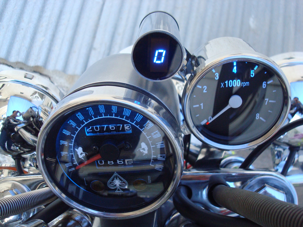
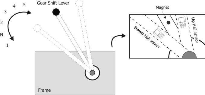
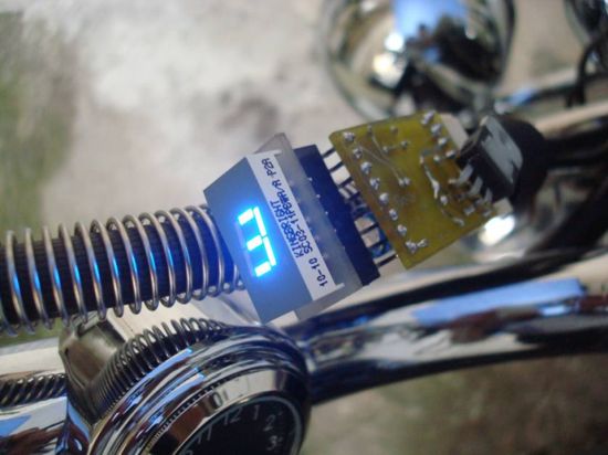
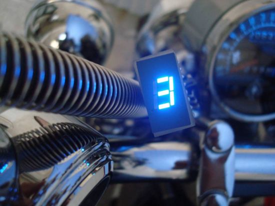
This is a new design for a universal gear indicator that can be fitted to any motorcycle as an aftermarket accessory. Its main advantage is that its operation depends entirely on the gear shift lever movement, instead of connecting to speedometer and tachometer sensors (found in expensive commercial devices), which are rarely available in older motorcycles. It consists of a main circuit including a 7‑segment LED indicator, two Hall sensors that are attached to the motorcycle frame, and a small magnet placed on the gear shift lever.

Image_1

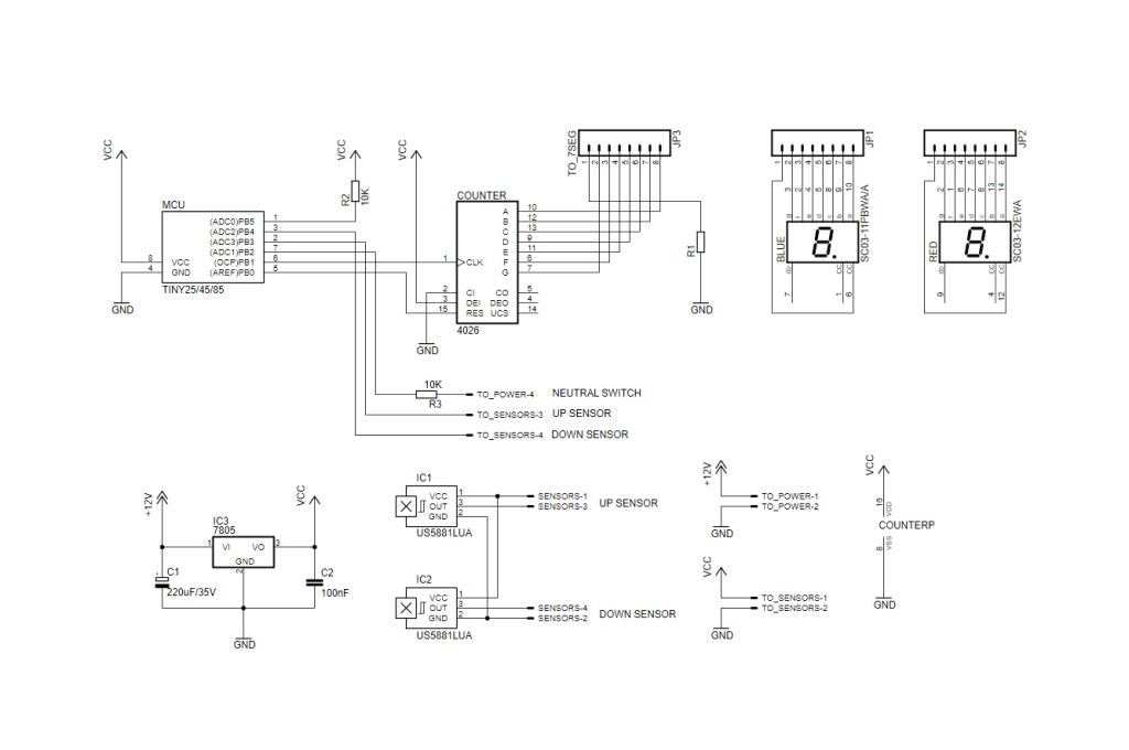
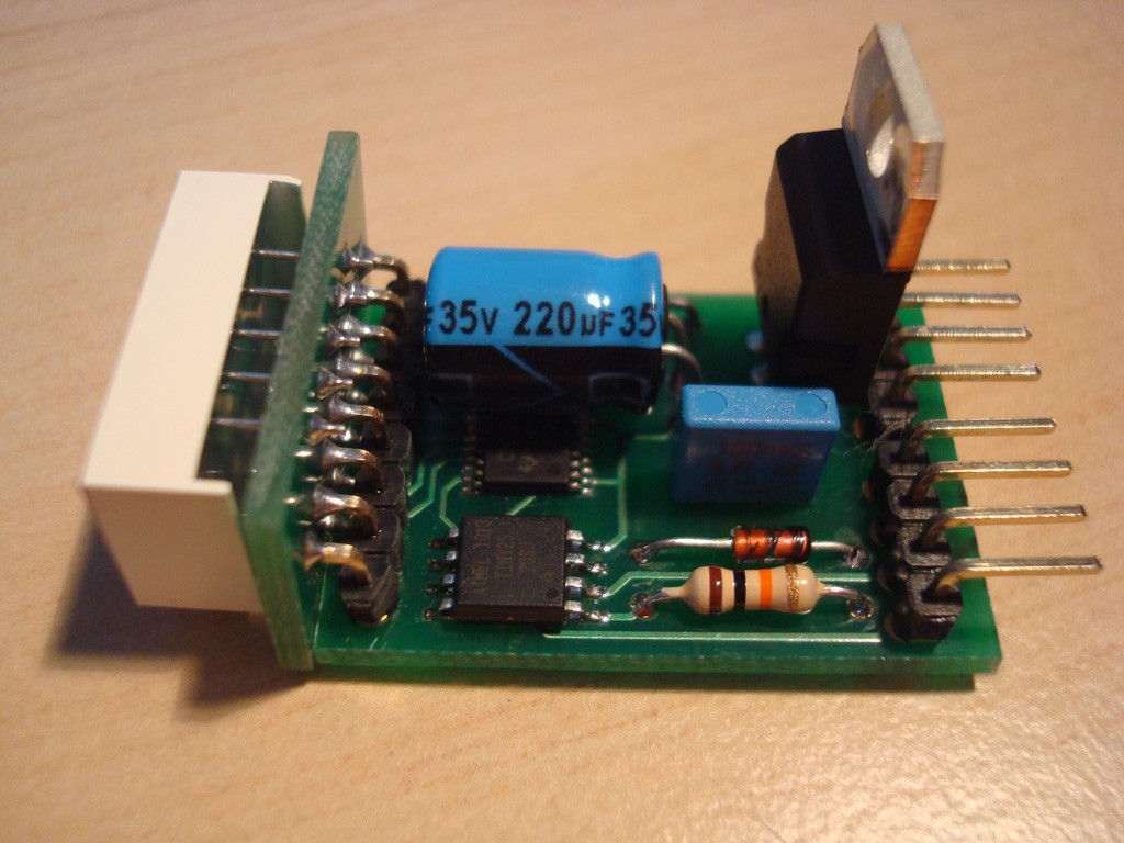
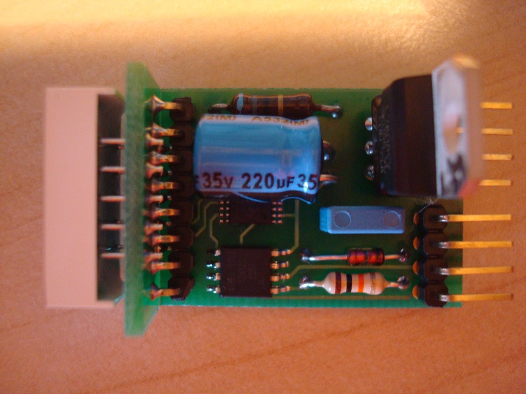
The main circuit is based on an AVR ATTINY25/45/85 microcontroller, which reads the signals of the two Hall sensors and the neutral switch and outputs the current gear number to a 7‑segment LED indicator, through a 4026 counter/decoder.

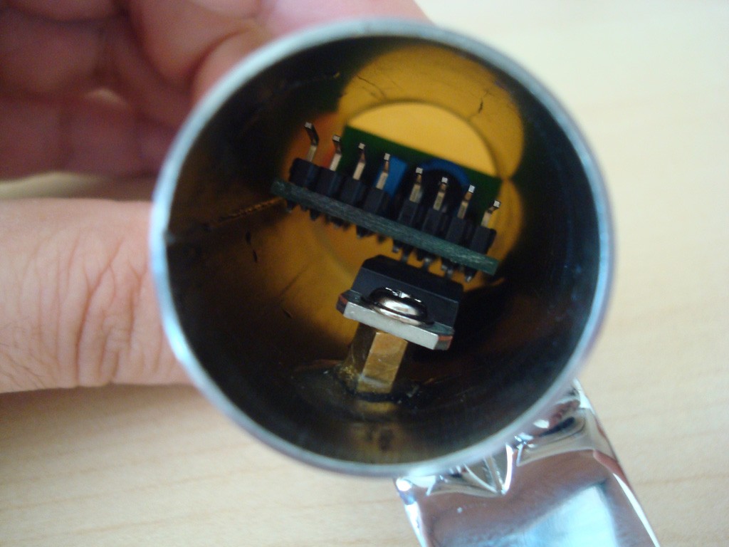
At maximum output power there is significant heat produced by IC1 and for that reason we mounted it directly on the ground plane to achieve maximum heat radiation.

Schematic

Source Code

The source code is written in AVR-GCC (WinAVR) and can be programmed with the default fuses using an AVR programmer (default : ATTINY25 microcontroller and USBTiny programmer). Moreover, the constant TOP_GEAR 5 should be changed to 6 for six-gear motorbikes. Source code can be downloaded on the download section below.

PCB Design

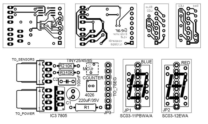
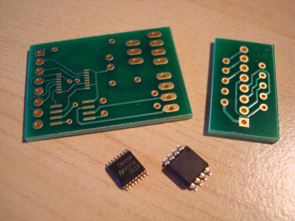
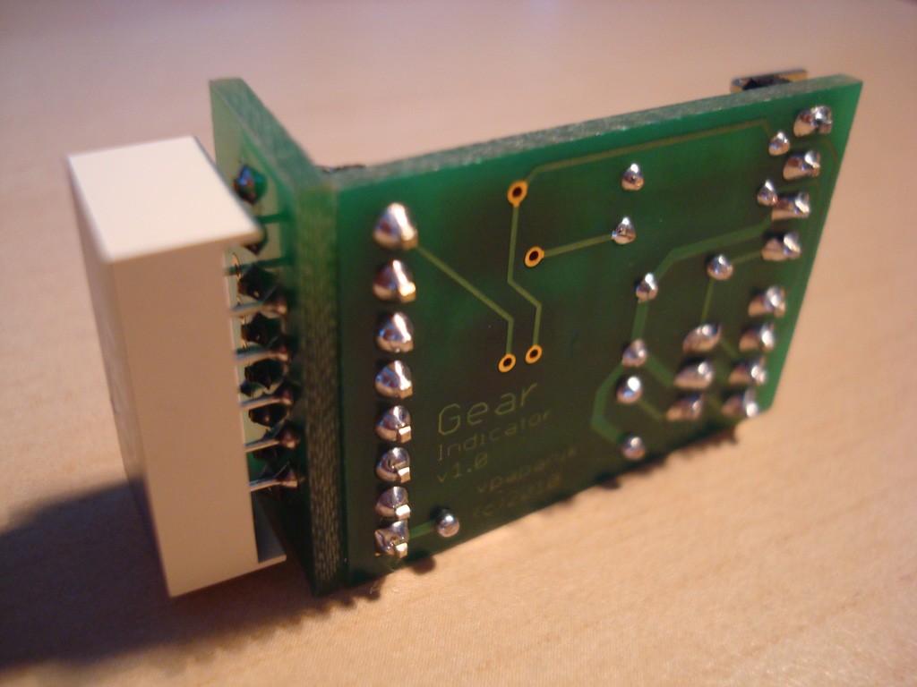
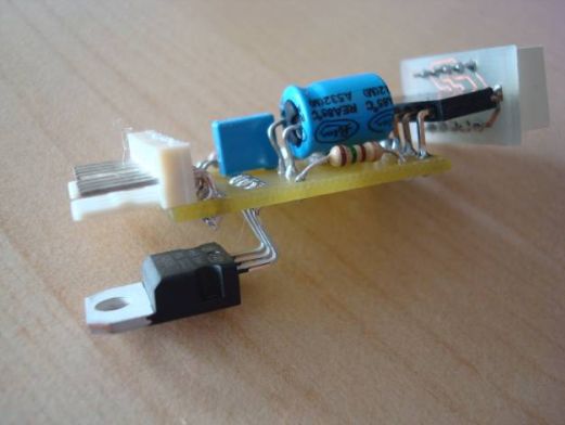
The suggested implementation for the main circuit is a small size, double-sided PCB, with SMD packages for the microcontroller and the decoder ICs. The 7-segment LED is placed in a secondary PCB, connected vertically to the main one in a modular fashion (see pictures). Two PCBs for different Kingbright LED footprints (red and blue) are also provided.

Image_3

Parts List

R1 10 to 220 Ω ½W Depending on preferred LED brightness
R2, R3 10 ΚΩ ¼W
C1 220 μF / 35V Electrolytic capacitor
C2 100 nF MKT/polyester capacitor
MCU ATTINY25/45/85 Mouser Part 556-ATTINY25-20SU
COUNTER 4026 Mouser Part 595-CD4026BPWE4
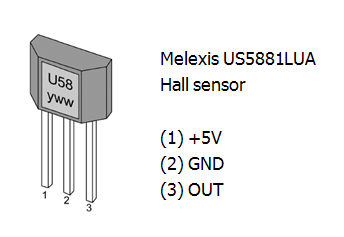
IC1, IC2 Hall sensor Melexis US5881LUA
IC3 7805 5V Regulator TO-220
BLUE Kingbright 0.3″ Mouser part 604-SC03-11PBWA/A
RED Kingbright 0.3″ Mouser part 604-SC03-12EWA
JPx Pin connectors As shown in silkscreen and pictures

Possible improvement

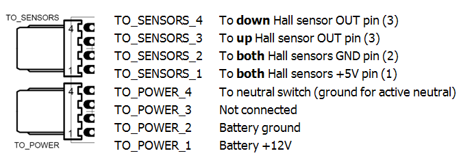
In the current design, when the neutral switch is open (there is a gear on), there appears to be a very small current (< 0.5 mA) sinking through R3, due to the voltage difference between the neutral switch connection (TO_POWER-4) and the microcontroller. If the neutral indicator is of LED type (not a resistor bulb), there is a possibility that it stays dimmed, instead of being completely off. In that case, a small switching diode (1N4148) can nicely replace R3 (on the same PCB) in order to block this small incoming current when the neutral switch is open, as shown in the figure below :

Image_15

For a better insight in the above issue, the following script can be imported in Paul Falstad’s excellent circuit simulator:

http://www.falstad.com/circuit

$ 1 5.0E-6 10.20027730826997 62 5.0 50
R 192 96 192 48 0 0 40.0 5.0 0.0 0.0 0.5
R 512 96 512 48 0 0 40.0 12.0 0.0 0.0 0.5
r 192 96 192 176 0 10000.0
x 231 142 309 145 0 12 internal pullup
x 125 25 277 31 0 24 Gear Indicator
x 456 26 571 32 0 24 Motorcycle
M 192 176 96 176 0 2.0
x 65 157 118 160 0 12 AVR Input
w 192 176 192 256 0
162 512 96 512 160 1 2.1024259 1.0 0.0 0.0
r 512 160 512 256 0 470.0
d 512 320 512 400 1 0.805904783
x 413 388 499 391 0 12 protective diode
s 512 400 640 400 0 1 false
g 640 400 640 448 0
x 539 422 615 425 0 12 neutral switch
x 309 240 391 246 0 24 1N4148
x 132 377 269 380 0 12 in place of R3, and watch
d 304 256 400 256 1 0.805904783
r 304 336 400 336 0 10000.0
x 337 371 367 377 0 24 R3
S 192 320 272 320 0 1 false 0
w 192 256 192 320 0
w 304 256 272 256 0
w 272 256 272 304 0
w 304 336 272 336 0
w 400 256 400 304 0
w 400 304 448 304 0
w 400 336 400 304 0
w 448 304 512 304 0
w 512 304 512 320 0
w 512 304 512 256 0
x 131 359 276 362 0 12 flip switch to insert a diode
x 134 394 272 397 0 12 current drop to zero when
x 134 412 254 415 0 12 neutral switch is open

… or click here for direct Circuit Simulator Link
Contributed by Brett Walach

Photos

B

C

D

E

Connections

Image_8

Image_9

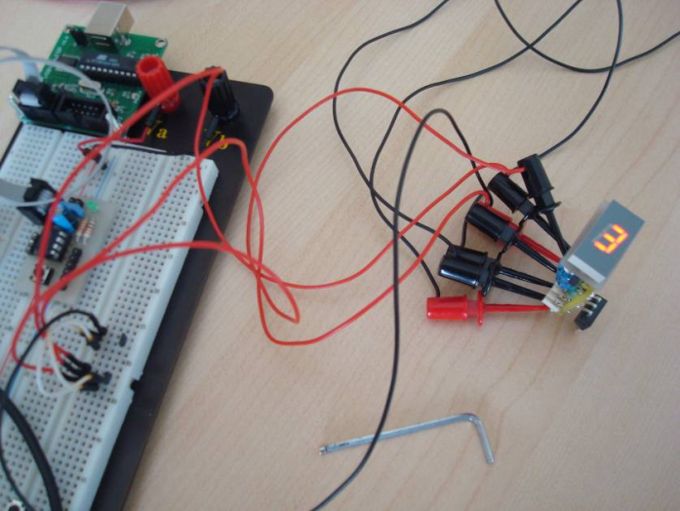
A successful circuit build will do a self-test when connected solely to 12V power (pins TO_POWER_1 and TO_POWER_2), by cycling through all digits on the 7-segment display (see video below). After the self-test, the current gear will be shown and can be changed by the shift lever movement. Note that a gear is changed when the magnet’s south pole is drawn away from the sensor (north pole will not work). Moreover, if a neutral gear is detected (from the neutral switch connected to TO_POWER_4), the display resets to zero (also acting as a self-calibrating feature if anything goes wrong). Finally, when the power is turned off, the last shown gear is stored in the MCU’s flash EEPROM and restored when the device is turned on again.

Image_10

The following video shows the initialization procedure of the gear indicator :

Self_Test

Sensor Cable

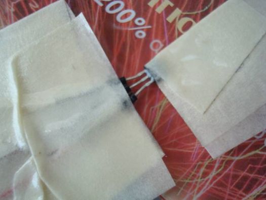
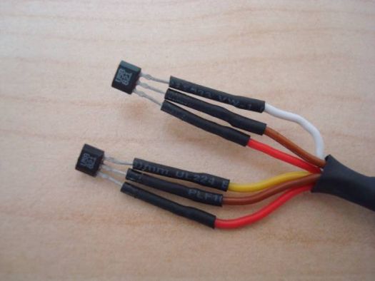
The following photos show the construction of the 4-wire sensors cable that is plugged to the TO_SENSORS connector. The visible sensor pin parts should be covered with plastic lacquer for protection as well.

Image_13

Image_14


After putting it all together the circuit is now operative and ready to be installed on the motorcycle. A video showing a simulation of gear shifting (by hand) is available below :

Circuit_Operation

Installation Photos

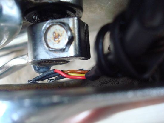
Here are some photos and videos from the installation on my Suzuki Intruder VS400

Image_16

Image_17

Image_18

Image_19

Image_20


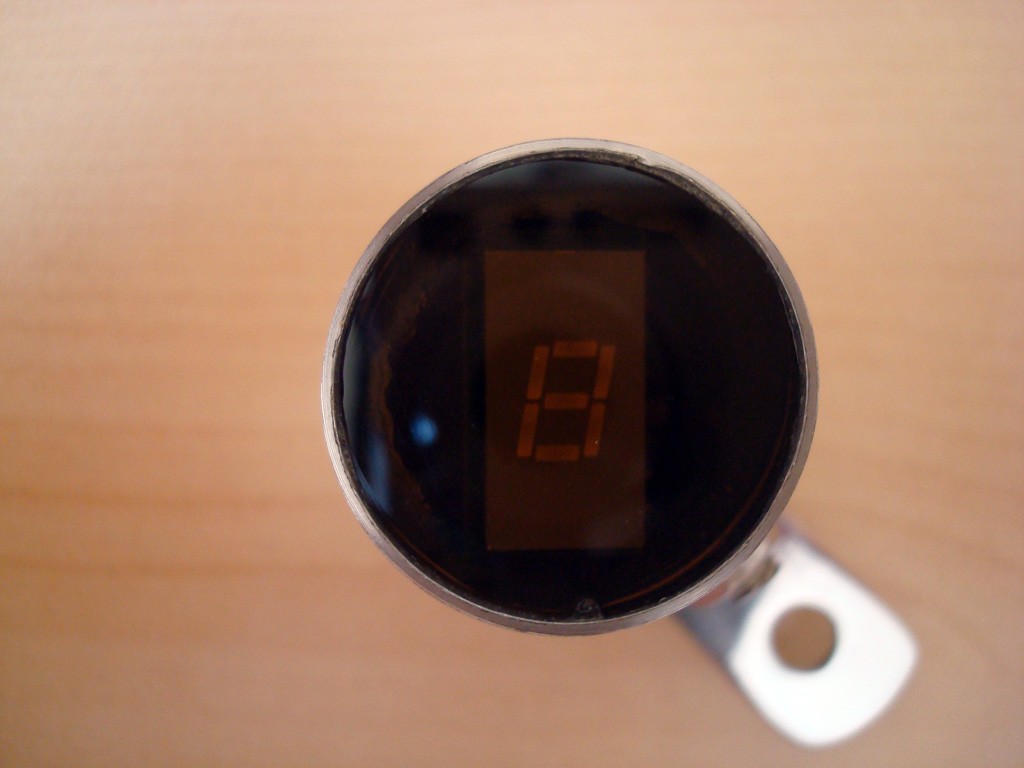
Custom Housing

G

H

Image_5


Installation Videos

Installation1 – Gear shifting by hand

Installation2 Real gear shifting with engine on

Installation3 – Storing last gear in EEPROM


Thanks for reading !

Designed and built by Vassilis Papanikolaou © 2010

PIC16F84A discolight effect with bass beat control

Moonflower

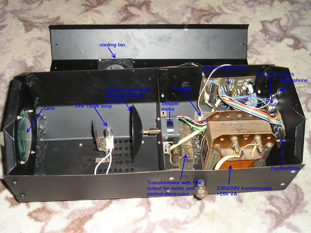
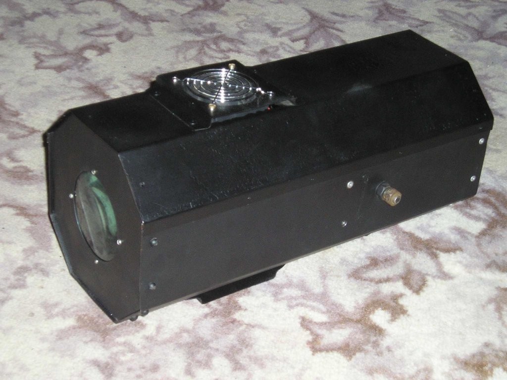
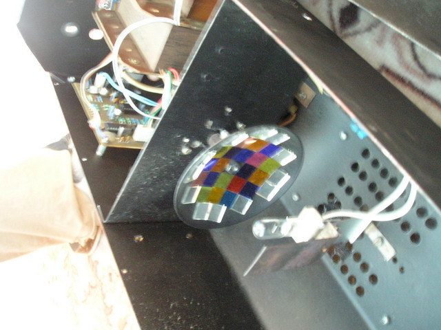
This is an early picture of my discolight effect. Because of the AGC circuit theres no need for potentionmeters for sensitivity adjust. I replaced them with trimmers. Now the microphone is on the control electronics because theres no need to place it outside the box and the possible noises from the surroundings are reduced.

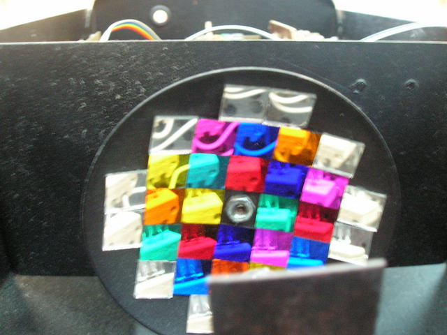
You have to choose the distance between Lens-Lamp-Parabola to get sharp beams. Its all about optics.That little ΄wall΄(hindrance) before the Lamp doesnt let the white light to pass through the Lens.

I have that box from a friend who had there a bigger home-made parabola. So the box with mine could be smaller but i didnt want to resize it.Its OK.

Introduction

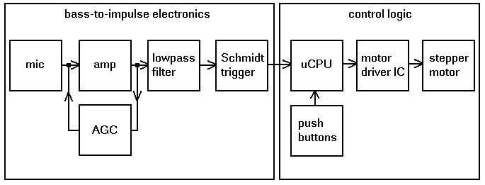
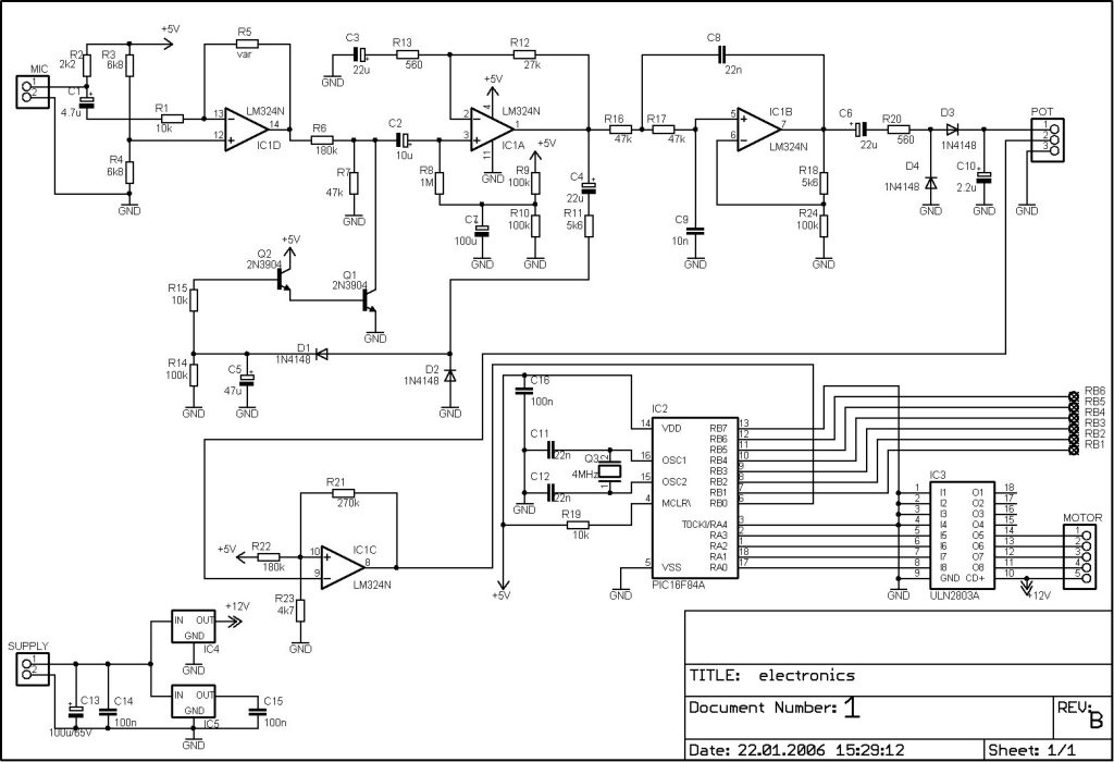
External circuit converts bass beat of music into pulses.The motor is controlled by them.
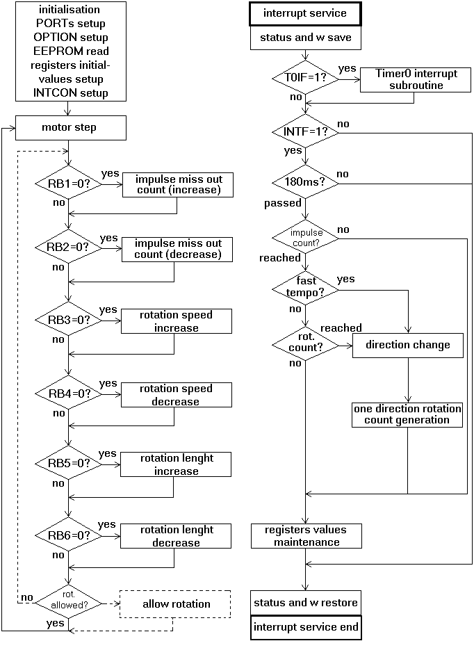
If theres bass beat recognised then the motor rotates one direction(in full stepping) for a predefined time then stops. If the second beat comes in then it rotates again for the same time and so on.There is a random number generator (from 1 to 4) written into the code which tells how many times have the motor to rotate one direction.After that the PIC changes rotation direction of the motor.If the tempo is too fast (<400msec) then the direction is changed immediately.
When the motor stops after the predefined time period a counter is enabled.if beat doesnt come in for 15sec the motor starts to rotate slowly in half stepping.If a beat comes in the counter is disabled and the motor continues its normal rotation in full stepping.
(Half stepping is smoother but unfortunately the torque is less)
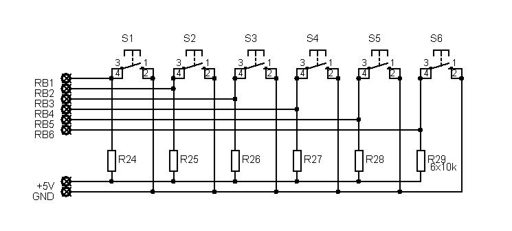
The PIC can control the motor after every beat or its possible to bypass some beats.It can be done by pushbuttons. Rotation speed and rotation lenght can be adjusted too.Settings are limited between values to prevent possible register overflow-underflow. These values are saved in EEPROM so after shut-down the settings dont lost.

A beat consist of a series of vibrations(dont know the correct english word for that-sorry) so the PIC gets a few
interrupts.To prevent multi-triggering theres a counter written into the code which disables reaction to beat for
200msecs after the first interrupt. 180msec delay is enough if you are using amplifiers output (or line out) as music source. I had to increase it to 200msec because i use microphone and the rooms echo influences operation.

Programming the PIC – Adjustments

When programming the PIC16F84A you need to fill the first three EEPROM locations with the setting values.
I used these one: 01 14 E0

I programmed the PIC with Ic-Prog using a simple JDM programmer.

After you succesfully built the whole hardware you need to adjust the trimmers very precisely. If you dont experiment a few times with adjusting them then its possible that the PIC will not recognise every beat because of the small amplifycation level. Or,it will do several things at only one beat.So you have to find the best adjustment.

The original circuit which converts bass beat into pulses is from Dan Frasers ΄Audio trigger circuit for light chasers΄
(updated by Tomi Engdahl). I only replaced the line-out control with microphone and removed the 555 circuitry
because of the software solution. The very-own in this project is the software for the PIC microcontroller.

Block diagram and software flowchart

block diagram

flowchart

Schematics

electronics

pushbuttons

Conclusion

megegykep

OLYMPUS DIGITAL CAMERA

OLYMPUS DIGITAL CAMERA

test action

This is my first PIC project.While I developed the code i learnt very much about coding a PIC. If you are interested in building it up please let me know!I would really like to know if my project is useful for other people too.

Synchronized multi-spark module (SMSM) for Electronic Ignition Devices (EID)

Schema

Multi-spark ignition is very useful especially in the case of startings at low temperature and at low rpm range. Basic idea, is to apply to spark plugs instead of only one spark, a “spark-burst” having big energy. In this case, combustion of air/fuel mixture is much better and the emissions are more reduced. In addition, through burning improvement, the consumption of fuel can be reduced.

Why synchronized multi-spark, or what means this?

Special literature abounds in multi-spark EID schematics. These have in common the fact, as the breaker-points don’t control directly EID, but an oscillator, which will generate a succession of impulses, and these impulses shall command EID. This aproach has two major deficiencies:

  1. First spark doesn’t match exactly with the moment of breaking points; so, it has an aleatory delay toward this. This is equivalent to an aleatory modification of ignition advance, which will leads to non-uniform run of engine.
  2. At high rpm range, the time between two impulses of multi-spark device can become comparable with the time between breaker-points impulses; this shall lead to an unstable operation of engine, with trepidations and knockings. To avoid this trouble, is necessary to switch-off the multi-spark device when rpm of engine exceeds a certain value.
    With these in mind, I imagined the device described forwards.

Few calculations elements

The crankshaft velocity of an internal combustion engine is given by following formula:

image_1

where :

n = revolution speed of engine crankshaft (rpm)
M = strokes number (2 or 4)
N = number of sparks per second (sparks frequency, in Hz)
B = number of ignition coils
C = cylinder number

For usual four stroke engines, with 4 cylinders and a single ignition coil, the formula becomes :

image_2

From where :

image_3

image_4

In fig.1 is shown an EID equipped with synchronized multi-spark module.

 image_5

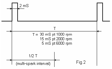
Shaping block has the role to provide fixed length impulses (2 mS) at each breaker-points opening. In this way are eliminated the false impulses which appear due contacts vibrations.
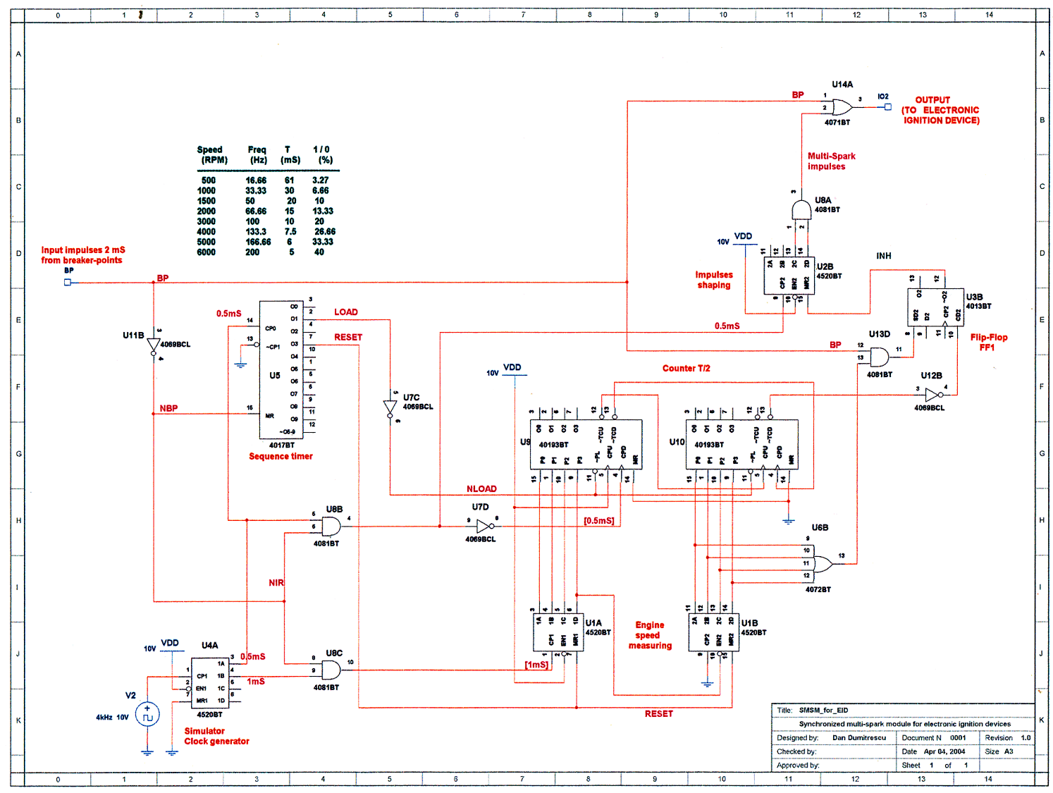
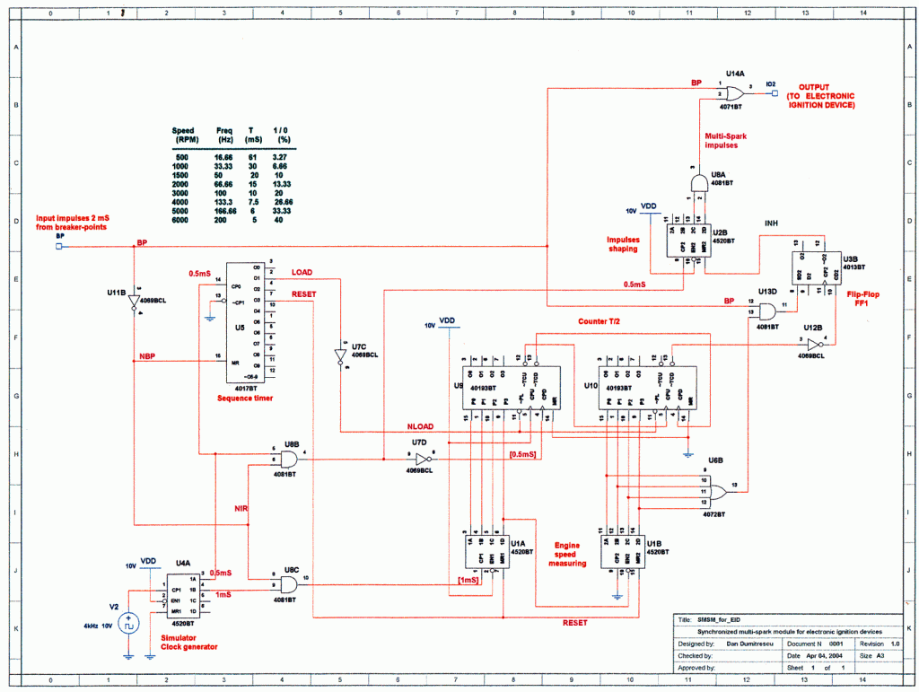
As shown in drawing, shaped impulse triggers directly the EID and act as START impulse for multi-spark module. If rpm of engine is under speed limit, the module will generate a series of supplementary impulses that, through an OR gate, will generate supplementary sparks by EID. When speed limit is reached (for example, 2000 rpm), supplementary impulses stops at module output, thus no supplementary sparks will be generated.

Functional description

The module uses for control the shaped impulses from breaker points. The time between two consecutively impulses depends on rpm engine and has the values shown in upper table.

image_6

From whole T interval, only in the first half of this will be generated supplementary sparks, after the main spark produced by the breaker points. This is very important, because generating sparks outside of half of the interval, the spinning distributor could apply these sparks to next cylinder, and this could be very harmful for mechanical parts of engine.

At breaker-points opening, the shaping circuit (not shown in drawing) produces a square impulse having 2 mS. This, named BP, is applied to EID by an OR gate and generate the main spark.


image_7

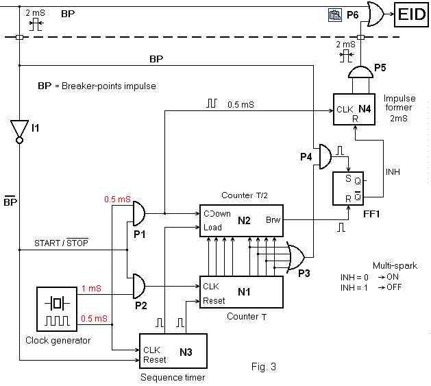
In fig. 3 is shown the block-diagram of the multi-spark module.

In multi-spark module, during 2 mS interval, a sequence timer (a counter with decoded outputs) accomplishes the initialization of circuits (full operations will be detailed later). When impulse BP disappears, the gate P2 is opened and the counter N1 receives impulses with 1 mS period, from clock generator. This 8 bits counter measures, in fact, the duration between two breaker-points impulses. It can count maximum 255 impulses, each having 1 mS (see the table, this correspond to 120 rpm, far below the free running speed !). At next BP impulse, P2 close and the counting stop. The number stored inside N1 is in fact the time length between two BP impulses.

The sequence timer “copy” the number stored in N1 to N2, after this resets counter N1. When BP becomes low level, N1 restarts the counting. In the same time, the up/down counter N2, starts counting the impulses having 0.5 mS period, which comes via gate P1. It counts down, but with double speed. In this way the counter N2 reach to “0” after T/2 time. The counter N4 and gate P5 makes the impulses for supplementary sparks (2 mS length).

This counter works only if INH signal is at low level. The fip-flop FF1 “marks” the interval T/2 in which will be generated supplementary sparks. It is reseted when N2 reach “0”. The gates P3 and P4 unlock the flio-flop and start supplementary sparks. Also, these gates switch-off the multi-spark function when engine speed limit is reached (in this case, ~ 2000 rpm). How works this ? In the upper table we can see at about 2000 rpm, the time length between two BP impulses is 15 mS.

This means as after a counting cycle, the first 4 bits of counter N1 will be 111 and next 4, 0000. In this case, P3 gate output will be at low level, and the same value for P4 output. The flip-flop FF1 will be not set, and as result, no supplementary sparks. If the speed engine decrease (time length T increase), the last 4 bits of N1 will have at least one 1 and the flip-flop will be set. This allow to appear supplementary sparks until flip-flop will be reseted by borrow impulse of N2.
The module can be maked like a plug-in adapter for an EID.

Nite Rider Lights

Nite_Rider_th


Description

The circuit is drawn with PCB 123 which you can download for free from http://www.pcb123.com

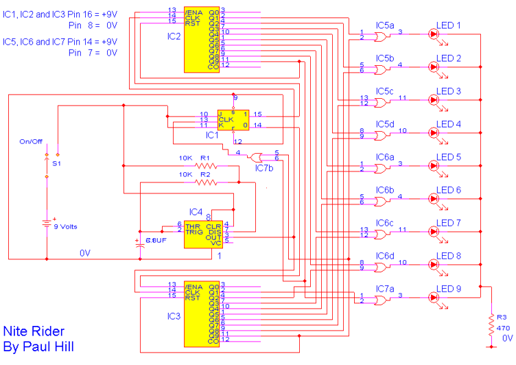
As a keen cyclist I am always looking for ways to be seen at night. I wanted something that was a novelty and would catch the motorists eye. So looking around at my fellow cyclists rear lights, I came up with the idea of ‘NITE-RIDER’. NINE extra bright LED’s running from left to right and right to left continuously. It could be constructed with red LEDs for use on the rear of the bike or white LED’s for an extra eye catcher on the front of the bike.

All IC’s are CMOS devices so that a 9V PP3 battery can be used, and the current drawn is very low so that it will last as long as possible.

Parts

Part Quantity Value
IC4 1 555 timer
IC1 1 4027 flip flop
IC2,IC3 2 4017 Decade Counter
IC5, IC6, IC7 3 4071 OR gate
R3 1 470 Ohm resistor 1/4 watt
R1, R2 2 10K resistors 1/4 watt
C1 1 6.8UF Capasitor 16V
LED1-LED9 9 Super brght LED’s
Battery 1 9V PP3 Battery
SW1 1 single pole switch

How it works

IC4, C1, R1 and R2 are used for the clock pulse which is fed to both the counters IC2 and IC3 Pin 14.

IC1 is a Flip Flop and is used as a switch to enable ether IC2 or IC3 at pin 13.

IC7a detects when ether IC2 or IC3 has reached Q9 of the counter pin 11.

IC5, IC6 and IC7a protects the outputs of the counters IC2 and IC3 using OR gates which is then fed to the Anodes of the LED’s 1 to 9.


Simple but reliable car battery tester

carbatterytester

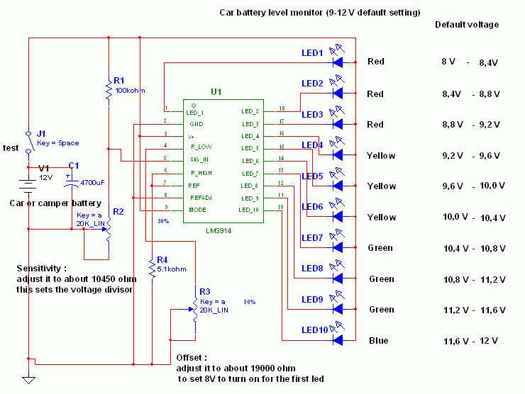
This circuit uses the popular and easy to find LM3914 IC. This IC is very simple to drive, needs no voltage regulators (it has a built in voltage regulator) and can be powered from almost every source.

Description

When the test button is pressed, the Car battery voltage is feed into a high impedance voltage divider. His purpose is to divide 12V to 1,25V (or lower values to lower values). This solution is better than letting the internal voltage regulator set the 12V sample voltage to be feed into the internal voltage divider simply because it cannot regulate 12V when the voltage drops lower (linear regulators only step down).

Simply wiring with no adjust, the regulator provides stable 1,25V which is fed into the precision internal resistor cascade to generate sample voltages for the internal comparators.  Anyway the default setting let you to measure voltages between 8 and 12V but you can measure even from 0V to 12V setting the offset trimmer to 0 (but i think that under 9 volt your car would not start). There is a smoothing capacitor (4700uF 16V) it is used to adsorb EMF noise produced from the ignition coil if you are measuring the battery during the engine working. Diesel engines would not need it, but i’m not sure. If you like more a point graph rather than a bar graph simply disconnect pin 9 on the IC (MODE) from power. The calculations are simple (default)
For the first comparator the voltage is : 0,833 V corresponding to 8 V
* * * * * voltage is : 0,875 V corresponding to 8,4 V


for the last comparator the voltage is : 1,25 V corresponding to 12 V

Have fun, learn and don’t let you car battery discharge… 😉

Automotive 12V to +-20V converter (for audio amplifier)

smps

The limitation of car supply voltage (12V) forces to convert the voltages to higher in order to power audio amplifiers.

In fact the max audio power x speaker (with 4 ohm impedance) using 12V is (Vsupply+ – Vsupply-)^2/(8*impedance) 12^2/32 = 4.5Watts per channel, that is laughable…

For powering correctly an amplifier the best is to use a symmetric supply with a high voltage differential. for example +20 – -20 = 40Volts in fact 40^2/32 = 50 Watts per channel that is respectable.
This supply is intended for two channels with 50W max each (of course it depends on the amplifier used). Though it can be easily scaled up or the voltages changed to obtain different values.

Overview – How it works

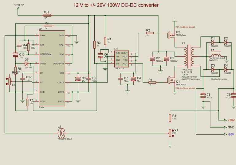
It is a classic push-pull design , taking care to obtain best symmetry (to avoid flux walking). Keep in mind that this circuit will adsorb many amperes (around 10A) so take care to reinforce power tracks with lots of solder and use heavy wires from the battery or the voltage will drop too much at the input.

The transformer must be designed to reduce skin effect, it can be done using several insulated magnet wire single wires soldered together but conducting separately. The regulation is done both by the transformer turn ratio and varying the duty cycle. In my case i used 5+5 , 10+10 turns obtaining a step up ratio of 2 (12->24) and downregulating the voltage to 20 via duty cycle dynamic adjust performed by the PWM controller TL494.

The step-up ratio has to be a little higher to overcome diode losses, winding resistance and so on and input voltage drop due to wire resistance from battery to converter.

Transformer design

The transformer must be of correct size in order to carry the power needed, on the net there are many charts showing the power in function of frequency and core size for a given topology. My transformer size is 33.5 mm lenght, 30.0 height and 13mm width with a cross section area of 1,25cm^2, good for powers around 150W at 50khz.

The windings , especially the primary must be heavy gauged, but instead of using a single wire it is better to use
multiple wires in parallel each insulated from the other except at the ends. This will reduce resistance increase due to skin effect. The primary and secondary windings are centertapped, this means that you have to wind 5 turns, centertap and 5 windings again. The same goes for the secondary, 10 turns, centertap and 10 turns again.

The important thing is that the transformer MUST not have air gaps or the leakage inductance will throw spikes on the switches overheating them and giving a voltage higher than expected by turn ratio prediction, so if your voltage output (at fully duty cycle) is higher than Vin*N2/N1 – Vdrop diode, your transformer has gap (of course permit me saying you that you are BLIND if you miss it), and this is accompanied with a drastical efficiency reduction. Use non-gapped E cores or toroids (ferrite).

Output diodes, capacitors and filter inductor

For rectification i preferred to use shottky diodes since they have low forward voltage drop, and are incredibly fast.
I used the cheap 1N5822, the best alternative for low voltage converters (3A for current capability).

The output capacitors are 4700uF 25V, not very big, since at high frequency the voltage ripple is most due to internal cap ESR fortunately general purpose lytics have enough low esr for a small ripple (some tens of millivolts). Also at high duty cycle they are feed almost with pure DC, giving small ripple. The filter inductor on the secondary centertap furter increases the ripple and helps the regulation in asymmetrical transients.

Power switch and driving

I used d2pak 70V 80A 0.004 ohms ultrafets (Fairchind semiconductor), very expensive and hard to find. In principle any fet will work, but the lower the on-resistance, the lower the on-state conduction losses, the lower the heat produced on the fets, the higher efficiency and smaller the heatsinks needed. With this fets i am able to run the fets with small heatsinks and without fan at full rated power (100W) with an efficiency of 82% and perceptible heating and with small heating at 120W (some degrees) (the core starts to saturate and the efficiency is a bit lower, around 75%)

Try to use the lowest resistance mosfet you can put your dirty hand 🙂 on or the efficiency will be lower than rated and you will need even a small fan. The fet driver i used is the TPS2811P, from Texas instruments, rated for 2A peak and 200ns. Is important that the gate drive is optimized for minimal inductance or the switching losses will be higher and you risk noise coupling from other sources. Personally i think that twisted pair wires (gate and ground/source) are the best to keep the inductance small. Place the gate drive resistor near the Mosfet, not near the IC.

Controller

I used the trusty TL494 PWM controller with frequency set at around 40-60 Khz adjustable with a potentiometer. I also implemented the soft start (to reduce powerup transients). The adjust potentiometer (feedback) must be set to obtain the desired voltage. The output signals is designed with two pull-up resistors on the collector of the PWM chip output transistor pulling them to ground each cycle alternatively. This signal is sent to the dual inverting MOSFET driver (TPS2811P) obtaining the correct waveform.

Power and filtering

How i said before the power tracks must be heavy gauged or you will scarify regulation (since it depends of transformer step up ratio and input voltage) and efficiency too. Don’t forget to place a 10A (or 15A) fuse on the input because the car batteries can supply very high currents in case of shorts and this will save you face from a mosfet explosion in case of failture or short, remember to place a fuse also on the battery side to increase the safety (accidental shorts->fire, battery explosion, firemen, police and lawyers around). Input filtering is important, use at least 20000uF 16V in capacitors, a filter inductor would be useful too (heavygauged) but i decided to leave it..

Final considerations

This supply given me up to 85% efficiency (sometimes even 90% at some loads) with an input of 12V because i observed all these tricks to keep it functional and efficient. An o-scope would be useful, to watch the ripple and gate signals (watching for overshoots), but if you follow these guidelines you will avoid these problems.

The cross regulation is good but keep in mind that only the positive output is fully regulated, and the negative only follows it. Place a small load between the negative rail and ground (a 3mm led with a 4.7Kohm resistor) to avoid the negative rail getting lower then -20V. If the load is asymmetric you can have two cases:

  • More load on positive rail-> no problems, the negative rail can go lower than -20V, but it is not a real issue for an audio amplifier.
  • More load on negative rail-> voltage drop on negative rail (to ground) especially if the load is only on the negative rail.

Fortunately audio amplifiers are quite symmetrical as a load, and the output filter inductor/capacitors helps to maintain the regulation good during asymmetrical transients (Basses).

ATTENTION: Keep in mind that THIS IS NOT A PROJECT FOR A BEGINNER, IT CAN BE VERY DANGEROUS IN CASE OF PROBLEMS, NEVER BRIDGE, BYPASS OR AVOID FUSES THESE WILL SAVE YOUR BACK FROM FIRE RISK.

FOR FIRST TESTING USE A SMALL 12V power supply and use resistors as load monitoring switches heat and current consumption (and output) and try to determine efficiency, if it is higher then 70-75% you are set, it is enough. Adjust the frequency for best compromise between power and switching losses, skin effect and hysteresis losses

Bill Of Materials
=================
Design: 12V to 20V 100W DC-DC conv
Doc. no.: 1
Revision: 3
Author: Jonathan Filippi
Created: 29/04/05
Modified: 18/05/05

Parts List
— ——— —–
Resistors
———
2   R1,R2 = 10
4   R3,R4,R6,R7 = 1k
1   R5 = 22k
1   R8 = 4.7k
1   R9 = 100k

Capacitors
———-
2   C1,C2 = 10000uF
2   C3,C6 = 47u
1   C4 = 10u
3   C5,C7,C14 = 100n
2   C8,C9 = 4700u
1   C12 = 1n
1   C13 = 2.2u

Integrated Circuits
——————-
1   U1 = TL494
1   U2 = TPS2811P

Transistors
———–
2 Q1,Q2 = FDB045AN

Diodes
——
4   D1-D4 = 1N5822
1   D5 = 1N4148

Miscellaneous
————-
1   FU1 = 10A
1   L1 = 10u
1   L2 = FERRITE BEAD
1   RV1 = 2.2k
1   RV2 = 24k
1   T1 = TRAN-3P3S

Car battery Indicator

car5

1034

Description

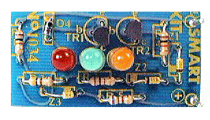
This is a really useful instrument for your car. It uses three LED’s to give a visual indication of the state of charge of your car battery. When the red LED is on the battery voltage is low, green is the OK signal and orange is a warning that the battery is overcharging. The whole circuit is accommodated on a small p.c. board and can be fitted easily anywhere in the dashboard.

Specifications

  • Working voltage: 12 V DC
  • Max. current: 40 mA

How it works

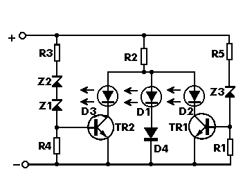
The principle behind the circuit is very simple. The first LED D1, is connected in series with R2 and D4 and will light when the battery voltage is below 11.5 V. If the voltage is above 12 V the zener Z3 will bias the transistor TR1 sufficiently to turn it on and this will light the second LED D2 which is green and indicates that the battery voltage is normal. As the collector to emitter voltage drop is less than the forward voltage drop of D4 the first LED does not get sufficient voltage across it to light and is turned off. If now the battery voltage rises above 13.5 volts then in a similar way the transistor TR2 is turned on and the third LED lights to indicate potential trouble. The zener diodes are used to provide the reference voltages for greater accuracy.

Schematic

1034d

Parts

R1, R4 10K
R2 470Ω
R3 100Ω
R5 680Ω
D1 red LED
D2 green LED
D3 orange LED
Z1,Z2 6,8V zener diode (1/2W)
Z3 11V Zener diode (1/2W)
TR1, TR2 BC548 – BC547 NPN Transistor


TOP PCB Companies