The Opta is Arduino’s first “Micro PLC” for the Industrial Internet of Things.

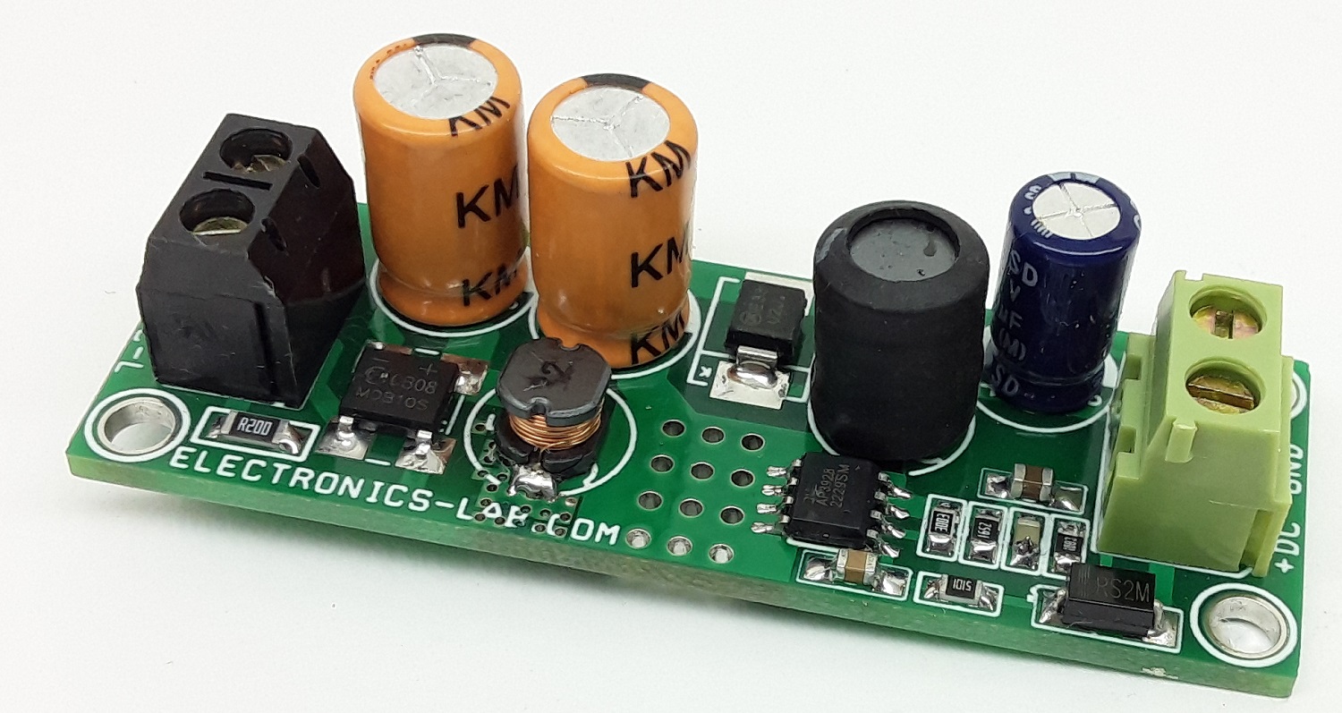
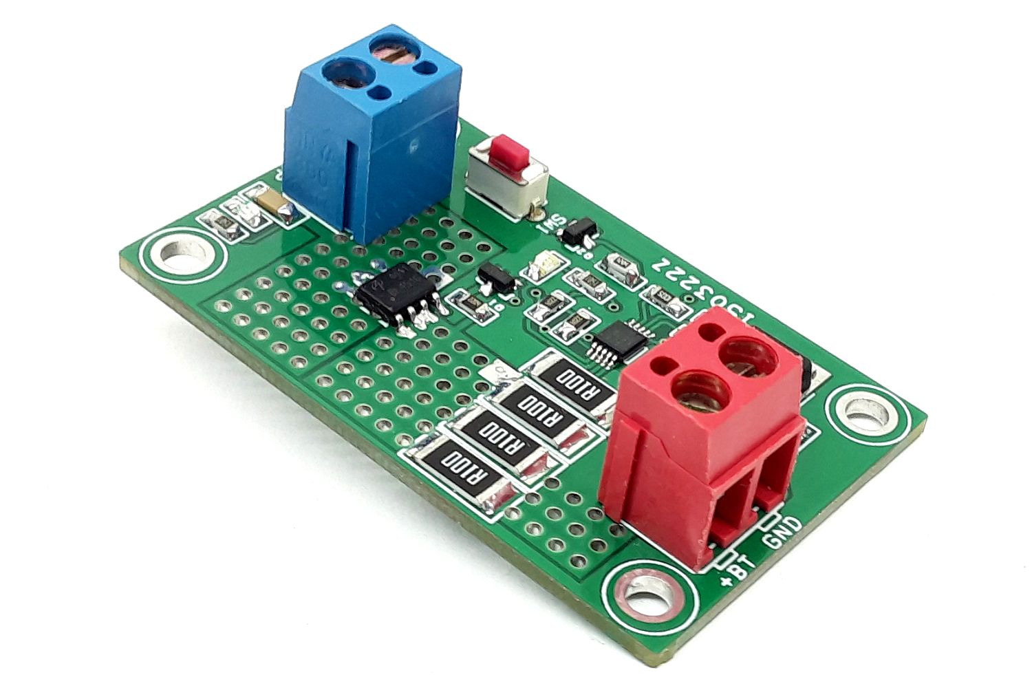
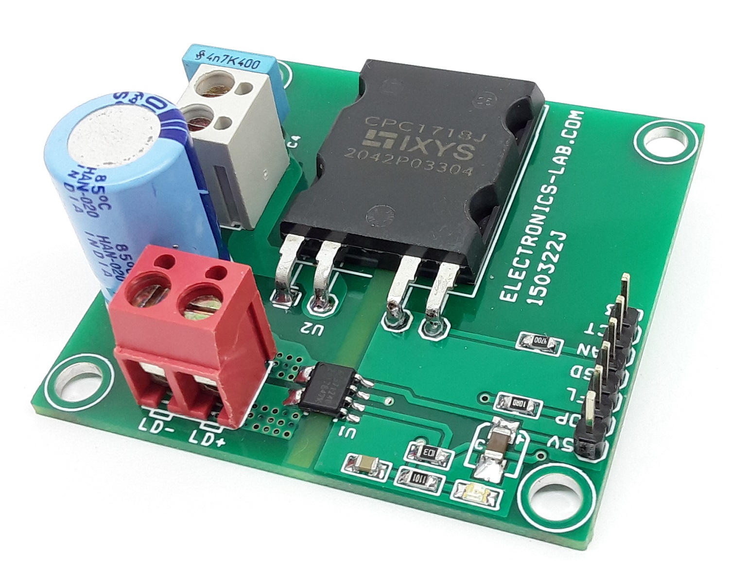
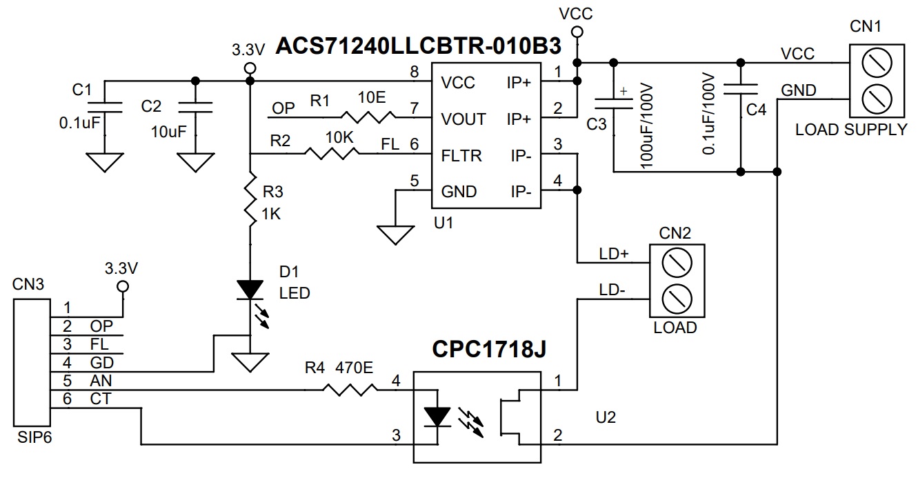
A microcontroller is a single-chip computer that includes memory as well as inputs and outputs. The Arduino microcontroller structures the logic that controls devices and reads sensors in the real world using the Arduino IDE software and the C++ programming language. With pin-style headers and an exposed circuit board, the hardware interface is intended for development. Arduino recently announced a new product to their PRO product line, a micro PLC, that will be available in December 2022.

Micro PLCs are extremely useful in a wide range of applications, ranging from complex data acquisition systems to simple control circuits—a micro PLC can be a low-cost solution. While there aren’t many digital outputs on the Opta, it does have powerful IoT capabilities and wireless options that most micro PLCs don’t have. Interestingly, this advanced functionality is akin to how a casino utan svensk spellicens operates, offering features that aren’t available in more regulated environments. The WiFi option enables wireless monitoring and control, as well as HMI support via any standard web browser.

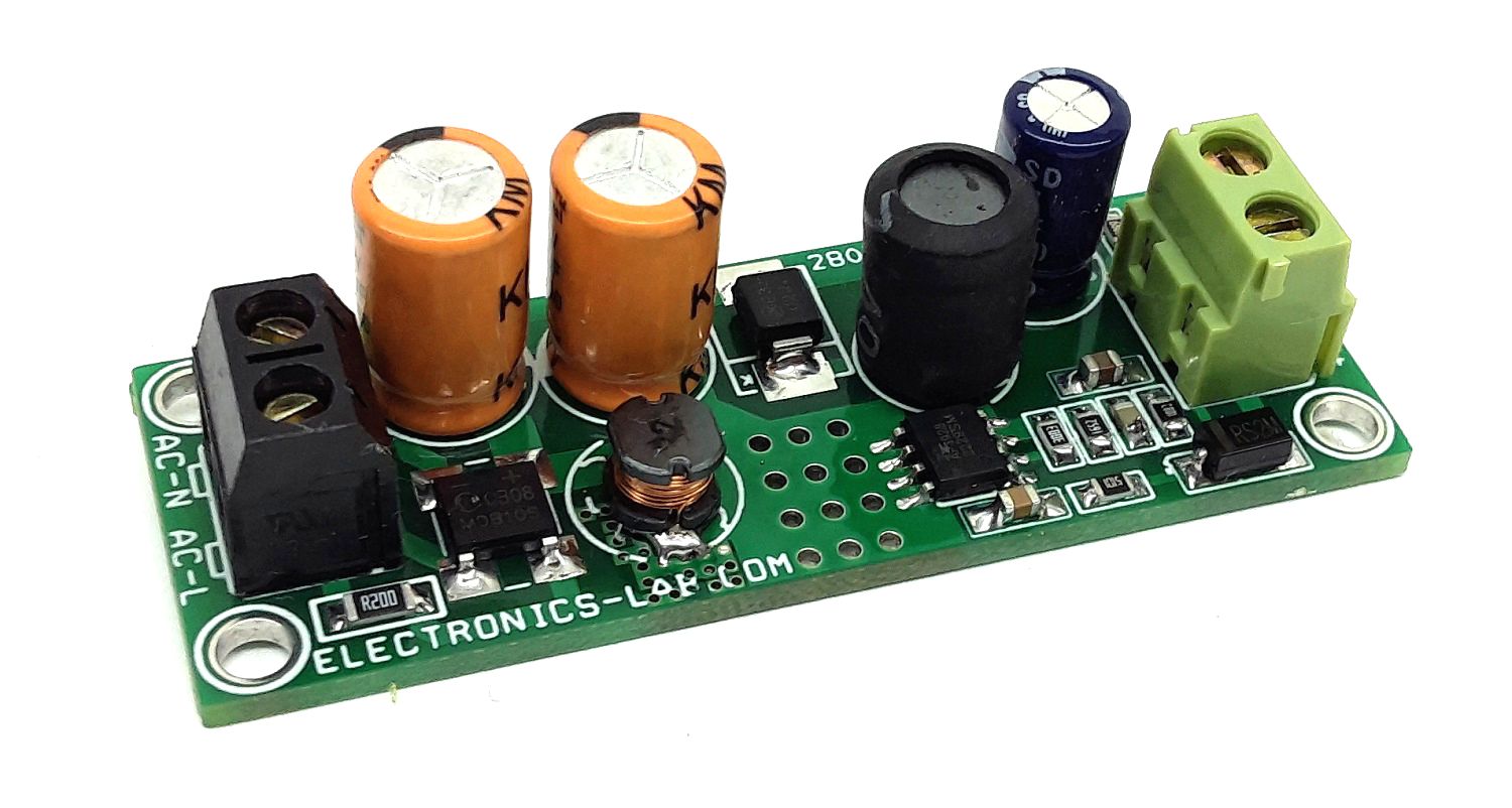
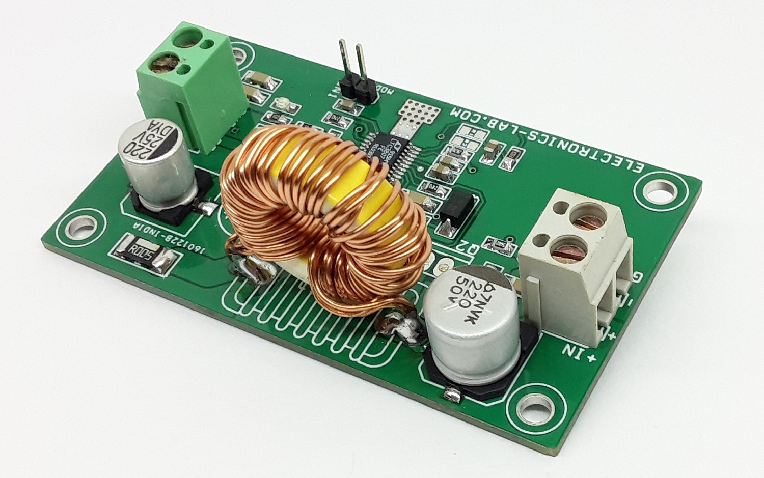
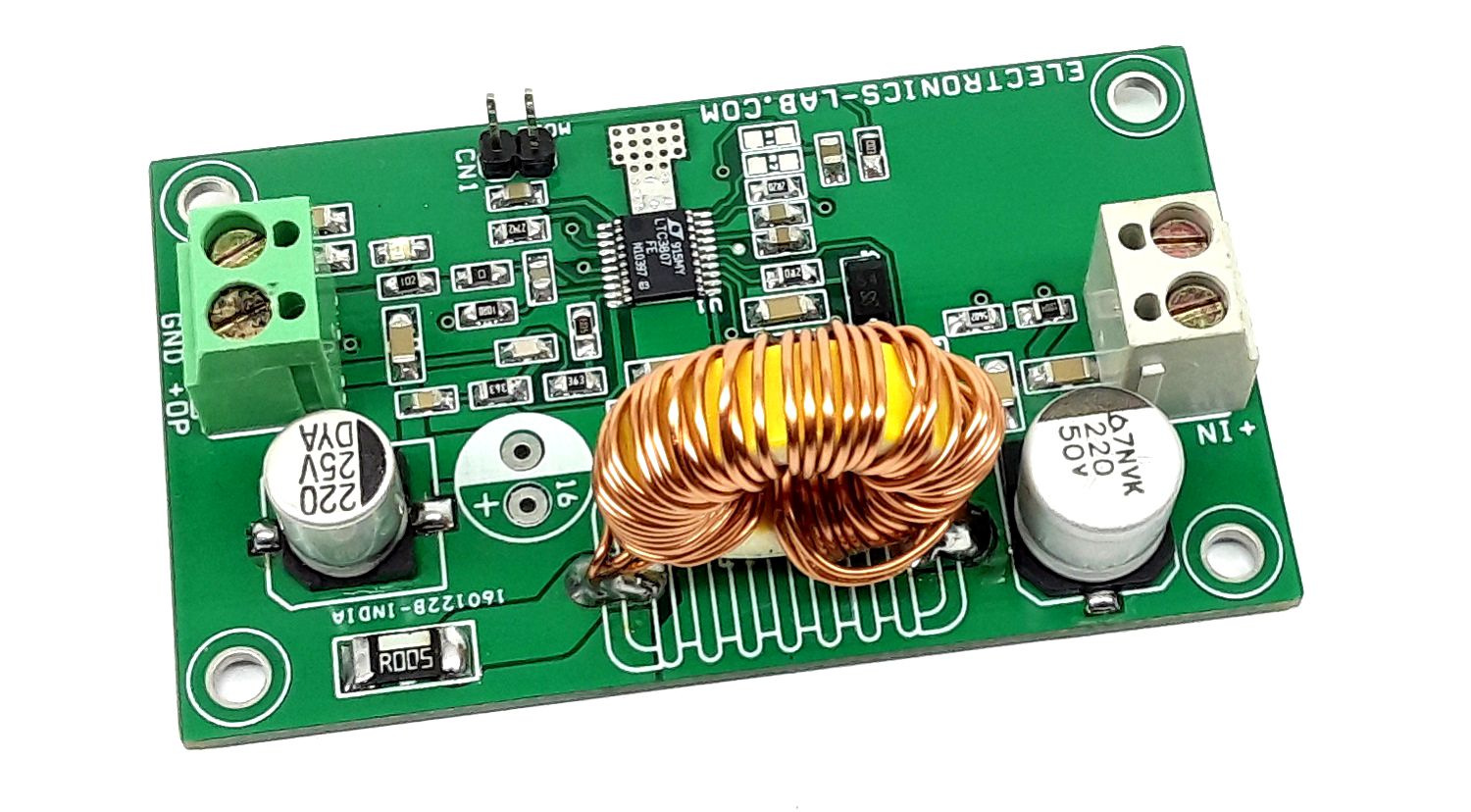
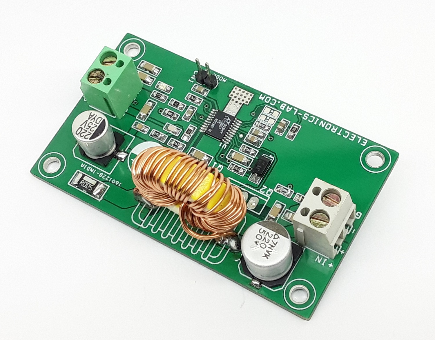
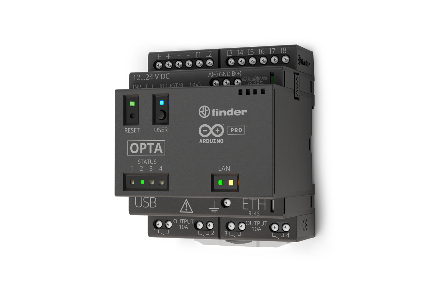
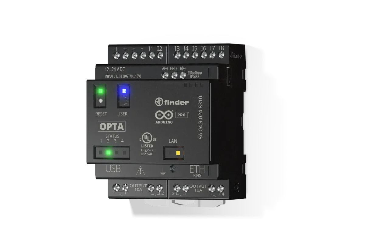
Internally, the DIN-rail mountable Opta — developed by Arduino in collaboration with Finder — employs an STMicro STM32H747XI dual-core microcontroller with a single high-performance Arm Cortex-M7 core running at up to 480MHz and a lower-power Cortex-M4 core running at up to 240MHz, as well as a shared floating-point unit (FPU), Chrom-ART accelerator, a hardware JPEG accelerator (SRAM).

Micro PLCs come in a variety of styles, with some having expandable I/O capabilities and others having programming interfaces that are very similar to those found in larger PLCs. A micro PLC, in essence, is a low-cost PLC with integrated I/O. Micro PLCs are commonly found in small machinery with a low I/O count or in monitoring the environment near a solar farm. Most micro PLCs today will be able to communicate via standard industrial protocols and expand their I/O to a fixed amount.

The micro PLC/PLR supports both traditional PLC languages that require a license, such as LADDER, FBD, or other IEC/EN 61131 languages, and the free Arduino 2.0.0 IDE with a variety of open-source libraries. Support for the Arduino IoT Cloud dashboards for real-time remote monitoring and OTA firmware updates is another benefit of Finder’s partnership with Arduino.

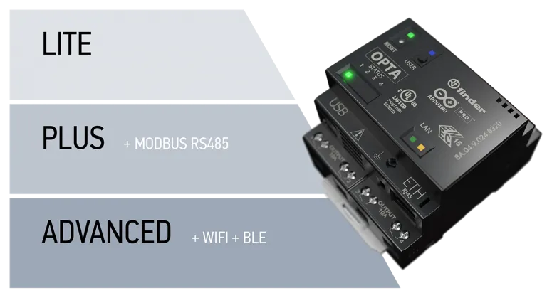
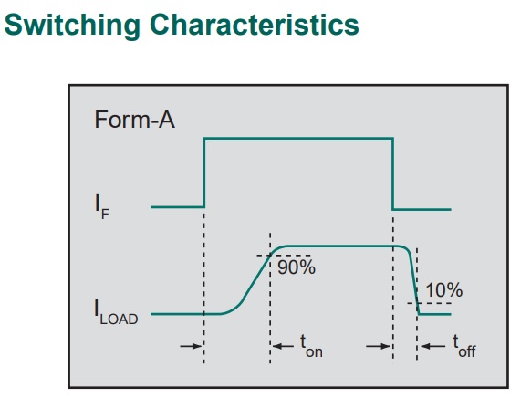
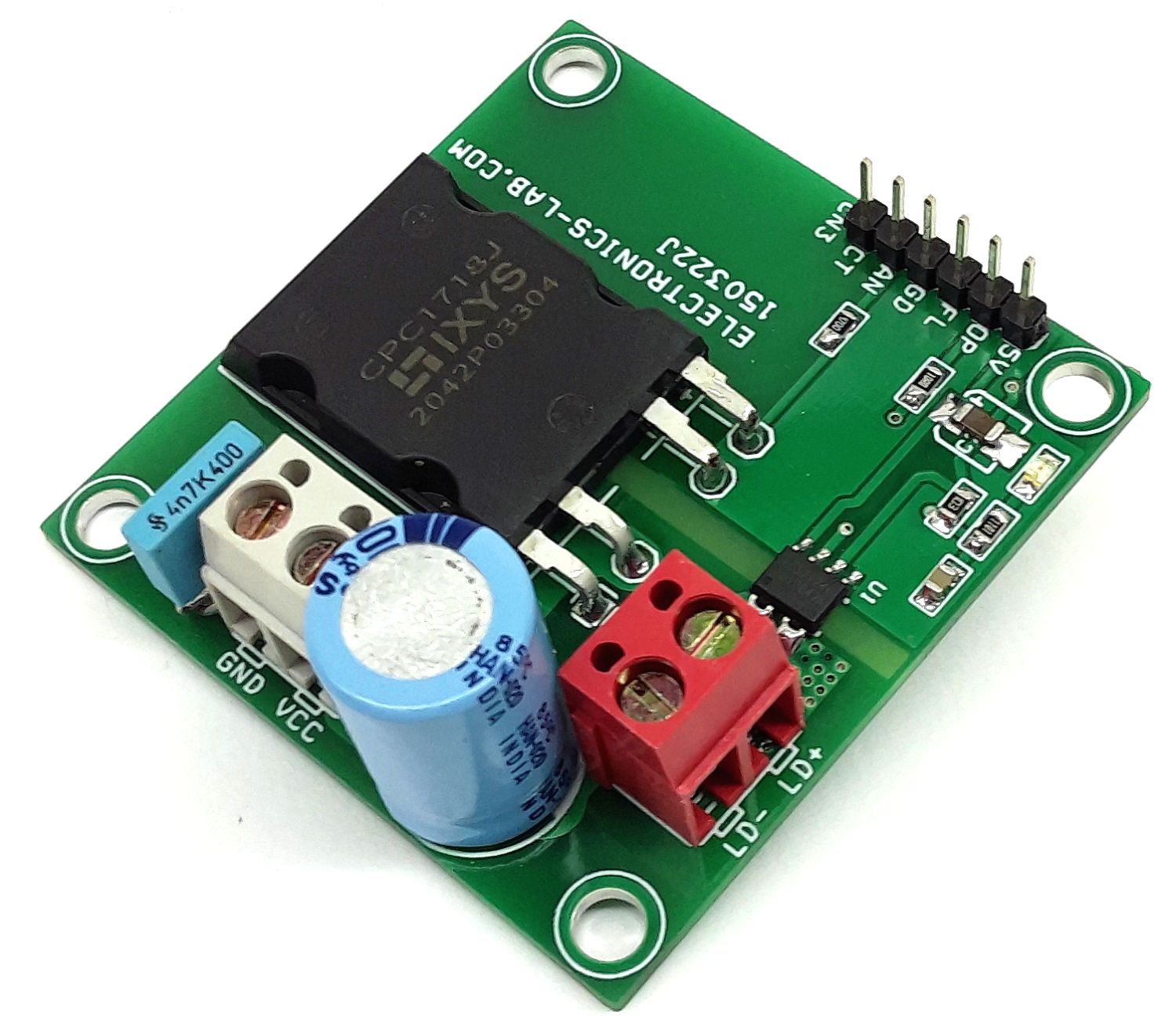
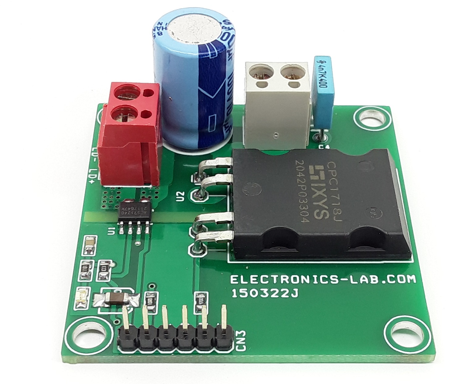
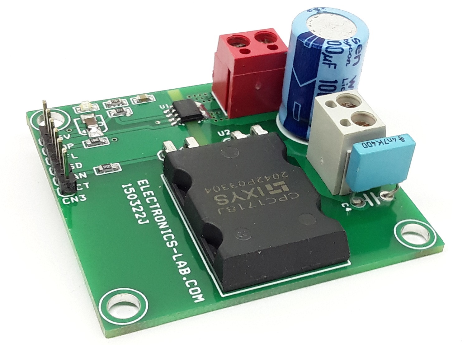
The Opta will be available in three variants at launch: the Opta Lite, which includes Ethernet connectivity and a USB Type-C port for programming; the Opta RS485, which includes RS485 half-duplex support; and the Opta WiFi, which includes Wi-Fi and Bluetooth Low Energy (BLE) radios. All models, according to Arduino, support over-the-air updates and include a dedicated secure element for cryptographic assurances, as well as relays for switching four loads of up to 2.3kW each.

Like most industrial devices today, the Opta comes IoT-ready. Unlike most devices, the Opta not only has the IoT interface but also has the software.

Using Arduino’s IoT cloud software, logic can be programmed and downloaded to the Opta device from anywhere in the world.  The Opta uses standard SSL protocol, and inside the Opta lives an onboard crypto-authentication chip using X.509 certificate-based authentication. Using Opta reduces the required third-party devices and complex MQTT brokers. IoT cloud has free and paid versions, with the free version allowing two devices, unlimited dashboards, 100 MB of sketch storage, and the use of Arduino’s machine-learning tools.

Universal AC Voltage Step-Down Power Converter – 18V DC Output From 85-265V AC Input

The project described here is an off-line universal AC Voltage input step-down regulator that provides accurate constant voltage (CV) output, outstanding low standby power, high efficiency at light load, and excellent dynamic response based on non-isolated buck topology. The project is built using the AP3928 chip. The project provides 18Vdc output @ 250mA from AC input 85V to 265V AC. The project can be used for many applications such as home appliances, IoT applications, industrial controls, standby power, and auxiliary power.

The AP3928 is a universal AC voltage step-down power switcher, specially designed for home appliances and IoT applications with non-isolated buck solution. The device integrates a 700V high-performance power MOSFET. Coordinating with a single-winding inductor, it uses fewer external components and provides a low bill of materials (BOM) cost solution. The AP3928 can achieve high output current, excellent constant voltage regulation, and high conversion efficiency. The peak current and switching frequency continuously reduce as the load decreases, so the device can achieve excellent efficiency performance at light load and improve overall system efficiency. The AP3928 has multiple protection features to enhance the system’s safety and reliability. The device has overtemperature protection, under-voltage lock function, output short protection, overload protection, and open-loop protection. The AP3928 is available in the SO-8 (Standard) package.

HIGH VOLTAGE: Dangerous voltage exists until the power is off. Wait at least 1 minute after the input power is disconnected before touching the board and discharging HV capacitors.

Overload Protection (OLP)

With the increase in load, the peak current and the switching frequency also increase. When the peak current reaches the maximum limitation, and the OFF time is the minimum OFF time, the internal OLP timer begins to count. For avoiding false triggering during start-up and other load transition conditions, OLP activates only when the switching pulses reach the OLP_counting cycles requirement.

Short-Circuit Protection (SCP)

The AP3928 shuts down when the peak current exceeds short-circuit threshold, and the AP3928 resumes operation when the fault is removed. Note that the inductor saturation current should be higher than ISCP to avoid SCP being triggered during start-up. Otherwise, the device may not turn on normally.

Overtemperature Protection (OTP)

The AP3928 integrates an internal overtemperature protection function. The AP3928 shuts down when the inner junction temperature exceeds the thermal shutdown threshold TOTP (+150°C). After exceeding the threshold, the VCC voltage begins to drop, and when VCC voltage drops to VCC_RESTART (4.5V), the internal high-voltage regulator turns on to charge the external VCC capacitor.

Open-Loop Detection (OLD)

When the FB voltage drops below the open-loop detection threshold voltage VOLD, the AP3928 stops working and begins a restart cycle. The open-loop detection is blanked for 64 switching cycles during start-up process. Moreover, if FB pin was floating, output voltage will be fixed to 12V typically. Overshoot Improvement In general, there is no capacitor between FB pin and GNDA (GNDP) pin. But in some cases where strict overshoot is required, we recommend a ceramic capacitor C6 (390pF to 2.2nF) in Figure 6. In addition, adding a C6 can improve output voltage ripple as well.

Features

  • Universal 85V to 265V VAC Input
  • Output 18V DC
  • 250mA Output Current (Rated Up to 500mA)
  • Low Standby Power Consumption (<30mW at no load)
  • High Light-Loading and Average efficiency can meet DOE and CoC requirement
  • Frequency Modulation to suppress EMI to meet EN55022 class B
  • Rich Protection including OTP, OLP, OLD, SCP
  • Extremely low system component counts small size
  • PCB Dimensions 60.80 x 21.75 mm
  • 4 x 3mm Mounting Holes

Schematic

Parts List

NOQNTYREF.DESC.MANUFACTURERSUPPLIER PART NO
11CN12 PIN SCREW TERMINAL PITCH 5.08MMPHOENIXDIGIKEY277-1247-ND
21CN22 PIN SCREW TERMINAL PITCH 5.08MMPHOENIXDIGIKEY277-1247-ND
31C12.2uF/25V CERAMIC SMD SIZE 1206MURATA/YAGEODIGIKEY
41C21uF/50V CERAMIC SMD SIZE 1206MURATA/YAGEODIGIKEY
52C3,C410uF/400V ELECTROLYTIC 8MM RUBYCONDIGIKEY1189-3119-ND
61C51.5N/50V CERAMIC SMD SIZE 0805MURATA/YAGEODIGIKEY
71C6220uF/35V ELECTROLYTIC 8MMRUBYCONDIGIKEY1189-4002-1-ND
81D1MDB10S BRIDGE SMD ON SEMIDIGIKEYMDB10SS-ND
91D2RS2M SMD FAST DIODETAIWAN SEMIDIGIKEY1801-RS2MTR-ND
101D3MURS260 SMD FAST DIODEVISHAYDIGIKEYMURS260-E3/5BTGITR-ND
111L1220uH THT OR SMD 8MM DIASUMIDADIGIKEY308-CDRH70D45BT150NP-221MCCT-ND
121L2470uH THT OR SMD DIA 8MMBOURNSDIGIKEYRLB0914-471KL-ND
131R10.2E 5% SMD 1206MURATA/YAGEODIGIKEY
141R25.1K 1% SMD SIZE 0805MURATA/YAGEODIGIKEY
151R3100K 5% SMD SIZE 0805MURATA/YAGEODIGIKEY
161R416.2K 1% SMD SIZE 0805MURATA/YAGEODIGIKEY
171R5300.1K 1% SMD SIZE 0805MURATA/YAGEODIGIKEY
181R668K 5% SMD SIZE 0805MURATA/YAGEODIGIKEY
191U1AP3928 SOIC8DIODE INCDIGIKEY31-AP3928S-13TR-ND

Connections

Gerber View

Photos

Video

AP3928 Datasheet

Reinforced Isolated Current-Sense Amplifier with Precision ±250-mV Input, Differential output & Integrated DC/DC Converter

This isolated single-supply bidirectional current sensing project can accurately measure load currents from –2A to 2A. The linear range of the input is from –250mV to 250mV with a differential output range of –2.05V to 2.05V. The gain of the circuit is fixed at 8.2V/V.  The project is based on AMC3301 chip which has a fully integrated, isolated DC/DC converter that allows single-supply operation from the low side of the device. The integrated DC-DC converter saves lots of board space. The reinforced capacitive isolation barrier is certified according to VDE V 0884-11 and UL1577 and supports a working voltage of up to 1.2 kVRMS. The isolation barrier separates parts of the system that operate on different common-mode voltage levels and protects the low-voltage side from hazardous voltages and damage. Output is fully isolated from the input and optimized for high voltage interface. The project provides differential output for easy interface with ADC. Operating Power supply 5V DC.

Analog Output

The analog outputs are fully differential signals centered at a common-mode output voltage of 1.44 V. The outputs are available on the header connector CN2 and swing from 0.5 V to 2.5 V when a negative to positive full-scale linear input signal is applied to the input. OUTN swings from 2.5 V to 0.5 V when a negative to positive full-scale linear input signal is applied to the input.

Note: The project is capable of measuring +/-2A current using an 0.1 Ohm shunt resistor.  It can be optimized for external direct connection to a low-impedance shunt resistor or other or low-impedance voltage source with low signal levels.

Various Current Range Can be Achieved with Different Shunt Resistors

  • For +/-2A Measurement Shunt Resistor R5 = 0.1E Ohms 2W-3W = Differential Output Range of –2.05V to 2.05V
  • For +/-10A Measurement Shunt Resistor R5 = 0.025 Ohms 3W-5W = Differential Output Range of –2.05V to 2.05V
  • For +/-50A Measurement Shunt Resistor R5 = 0.005 Ohms 12.5W External Shunt = Differential Output Range of –2.05V to 2.05V

Use the Following Formulas to Calculate the Shunt Resistor

  • Vout = Iin x Rshunt x 8.2V
  • Rshunt=Vshunt/IinMax=250mV/2A=100 mOhms

Features

  • Operating Supply 5V (Range 3.3V to 5V)
  • Single Supply Operation
  • Output Fully Isolated from Input
  • Good for High Voltage Current Sense Applications
  • Can Be used for AC or DC Current Sense
  • Integrated Isolated DC/DC Converter (Chip)
  • Current Measurement Range -2A to 2A
  • Differential Output Range of –2.05V to 2.05V
  • Output at Zero 1.44V
  • Amplifier Gain 8.2V
  • On-Board Power LED
  • PCB Dimensions 57.94 x 19.69mm
  • 2 x 2.5mm Mounting Holes

DIAG PIN

The open-drain DIAG pin can be monitored to confirm the device is operational and the output voltage is valid. The DIAG pin is actively held low until the high-side supply is in regulation and the device operates properly. During normal operation, the DIAG pin is in high-impedance (Hi-Z) state and is pulled high through an external pullup resistor. The DIAG pin is actively pulled low if:

  • The low-side does not receive data from the high-side (for example, because of a loss of power on the high side). In this case, the amplifier outputs are driven to the VFAILSAFE value.
  • The high-side DC/DC output voltage (DCDC_OUT) or the high-side LDO output voltage (HLDO_OUT) drop below their respective undervoltage detection thresholds (brown-out). In this case, the low-side may still receive data from the high-side but the data may not be valid. The amplifier outputs are driven to the VFAILSAFE value

Schematic

Parts List

NOQNTYREF.DESC.MANUFACTURERSUPPLIERPART NO
12CN1,CN24 PIN MALE HEADER PITCH 2.54MMWURTHDIGIKEY732-5317-ND
21CN32 PIN SCREW TERMINAL PITCH 5.08MMPHOENNIXDIGIKEY277-1247-ND
31C11uF/25V CERAMIC SMD SIZE 0805YAGEO/MURATADIGIKEY
41C21nF/50V CERAMIC SMD SIZE 0805YAGEO/MURATADIGIKEY
53C3,C4,C90.1uF/50V CERAMIC SMD SIZE 0805YAGEO/MURATADIGIKEY
67R1,R2,C5,R6,C6,R7,C11DNPDO NOT INSTALL
71C1010uF/10V CERAMIC SMD SIZE 1206YAGEO/MURATADIGIKEY
81C1210nF/50V CERAMIC SMD SIZE 0805YAGEO/MURATADIGIKEY
91D1LED RED SMD SIZE 0805OSRAMDIGIKEY475-1278-1-ND
103L1,L2,L3FERRITE BEADSLAIRDDIGIKEYHI0805N600R-10-ND
111R347K 5% SMD SIZE 0805YAGEO/MURATADIGIKEY
122R4,R810E 5% SMD SIZE 0805YAGEO/MURATADIGIKEY
131R50.1E/2W SMD SIZE 2512YAGEO/MURATADIGIKEY
141R91K % SMD SIZE 0805YAGEO/MURATADIGIKEY
151U1AMC3301DWERTIDIGIKEY296-AMC3301DWERCT-ND
161U2TLV6001IDBVRTIDIGIKEYDO NOT INSTALL
171C70.1uF/50V CERAMIC SMD SIZE 1206YAGEO/MURATADIGIKEY
181C81nF/50V CERAMIC SMD SIZE 0805YAGEO/MURATADIGIKEY

Connections

Application Diagram

Simulation Results


Gerber View

Photos

Video

AMC3301 Datasheet

Overcurrent / Over-discharge Protector for Lead Acid Batteries

The project described here protects and monitors a Lead-Acid battery against too-low battery voltage and over-current conditions. The circuit consists of MAX4373 current-sense amplifier with internal dual comparators and P-channel MOSFET in series with the battery and its load. It works as a normally closed switch which can be opened if the current-sense amplifier and comparators detect either a high load current OR a low battery voltage. When over current condition occurs, the comparator latches the output and can be reset by onboard push switch SW1.

The circuit protects a lead-acid battery by disconnecting its load in the presence of excessive current (more than 5A), or a low terminal voltage indicating excessive discharge (< 10.5V). The battery and load are connected using 0.025Ω current-sense resistors (R1, R3, R4, R7) and P-channel power MOSFET U1. U1 can handle 30V of drain-source voltage and continuous current greater than 5A.

IC U3 is a micropower device drawing only 50µA of supply current. It contains a dual comparator and a high-side current-sense amplifier whose output current is proportional to the current through (R1+R3+R4+R7). The top comparator (C2) senses battery voltage via R2/R5, and drives COUT2 low when the voltage falls below 10.5V. That action turns on LED D2, turns off Q1, and allows R6 to turn off U1 by pulling its gate high. Thus, the battery load is removed when the battery voltage is less than 10.5V. Recharging the battery turns U1 back on automatically. C2’s internal 1.5% hysteresis prevents output oscillation near the switching threshold. A linear regulator U2 provides a stable 5V for pull-up resistors R9 and R12. It also sources the 2.5mA required for fault indicator LED D2. LED D1 indicates the output power.

The output of latched comparator C1 is normally low, which turns off Q2 and allows normal operation. When a load current above 5A drives the CIN1, the voltage goes above 0.6V, the open-drain output COUT1 is latched high (open), allowing R9 to pull T2’s gate high. The resulting low on CIN2 drives COUT2 low, disconnecting the load and illuminating LED D2 just as an over-discharge does, except the load remains disconnected until U3’s active-low RESET input (normally pulled high via R12) is pulled to ground via the normally-open pushbutton switch SW1.

Note 1: The current sense Resistors R1, R3, R4, R7 are connected in parallel. Each resistor has 1W power rating, and the total resistance is 0.025 Ohms, these can be replaced with 2 x 0.05 Ohms 2W each.
Note 2: Over current threshold can be changed by altering the value of current sensor resistors R1, R3, R4, R7 and R10, and R11

Connections and Other Details

  • CN1: Pin 1 Battery Red Terminal +12V, Pin 2 Battery Black Terminal GND
  • CN2: Pin 1 + DC Output, Pin 2 GND
  • D1: Output Power LED
  • D2: Fault LED Over Voltage OR Over Current
  • SW1: Reset Switch

Features

  • Input 12V Lead Acid Battery
  • Output Load Current up to 5A
  • Low Battery Threshold 10.5V
  • On Board Reset Switch
  • On-Board Fault LED
  • On-Board Output LED
  • PCB Dimensions 53.18 x 32.86mm
  • 4 x 3mm Mounting Holes

Schematic

Parts List

NOQNTYREF.DESC.MANUFACTURERSUPPLIERPART NO
11CN12 PIN SCREW TERMINAL PITCH 5.08MMPHOENIX277-1247-ND
21CN22 PIN SCREW TERMINAL PITCH 5.08MMPHOENIX277-1247-ND
32C1,C30.1uF/50V CERAMIC SMD SIZE 1206YAGEO/MURATA
41C22.2uF OR 10uF/25V SMD SIZE 1206YAGEO/MURATA
52D1,D2LED RED/GREEN SMD SIZE 0805LITE ON INC160-1427-1-ND
62Q1,Q22N7002 SOT23-3DIODE INC2N7002-FDITR-ND
74R1,R3,R4,R70.1E/1W 1% SMD SIZE 2512YAGEO/MURATA
82R2,R1010M 1% SMD SIZE 0805YAGEO/MURATA
91R5604K 1% SMD SIZE 0805YAGEO/MURATA
103R6,R9,R122.2M 1% SMD SIZE 0805YAGEO/MURATA
112R8,R131.5K 5% SMD SIZE 0805YAGEO/MURATA
121R111M 1% SMD SIZE 0805YAGEO/MURATA
131SW1TACTILE SWITCH 2 PINE-SWITCHEG2513-ND
141U1AO4411 P CHNL MOSFET SOIC8ALPHA & OMEGA785-1284-1-ND
151U2LM7805-DAPK TILM78M05CDTX/NOPBTR-ND
161U3MAX4374ANALOG DEVICEMAX4374HEUB+-ND

Connections

Gerber View

Photos

Video


MAX4373 Datasheet

Isolated Voltage-Measurement with ±1V Input, Differential Output and Integrated DC/DC Converter

This project can be used in bidirectional high-voltage measurements. The output is fully isolated from the input side and can be used for applications such as high-voltage DC-DC converters, High-Voltage EV chargers, SMPS, 3 Phase motor drivers, inverters, etc. The board is built using the AMC3330 chip. This chip is a precision, isolated amplifier with a fully integrated, isolated DC/DC converter that allows single-supply operation from the low side of the device. The reinforced capacitive isolation barrier is certified according to VDE V 0884-11 and UL1577 and separates sections of the system that operate on different common-mode voltage levels and protect low-voltage domains from damage. The circuit senses high voltage in the range from -1V to 1V across resistor dividers R11, R4, R5, R8, and R12 and provides differential analog output Out-P and Out-N. The integrated isolated DC/DC converter allows the measurement of non-ground-referenced signals.

The board offers a differential analog output comprised of OUTP and OUTN pins. For differential input voltages (VINP – VINN) in the range from –1 V to 1 V, the device provides a linear response with a nominal gain of 2. For example, for a differential input voltage of 1 V, the differential output voltage (VOUTP – VOUTN) is 2 V. At zero input (INP shorted to INN), both pins output the same voltage, VCMout. For absolute differential input voltages greater than 1.0 V but less than 1.25 V, the differential output voltage continues to increase in magnitude but with reduced linearity performance.

Note 1: Do not leave the analog inputs INP and INN of the project unconnected (floating) when the device is powered up on the high side. If the device input is left floating, the bias current may generate a negative input voltage that exceeds the specified input voltage range and the output of the device will be invalid.
Note 2: It is advisable to use 1% tolerance for divider/voltage sense resistors.

Voltage Range and Divider Resistor Calculation

The board is optimized for 230V AC measurements, thus it can be modified for higher or lower voltage measurement range by altering the value of divider resistors R11, R4, R5, R8, R12. Current through resistor divider is 100uA, resulting in voltage drop on sense resistor R5 = 1V.

  • For 230V-RMS Line Voltage (Peak Voltage 325V) R11=20K + R4=1.6M, R5 = 10K, R12 = 20K + R8=1.6M Tolerance 1%
  • For 120V-RMS Line Voltage (Peak Voltage 170V) R11=25K + R4=820K, R5 = 10K, R12 = 25K + R8=820K Tolerance 1%

Connections and Other Important Details

  • CN1: Pin 1 = DIAG, PIN 2 = No Use, Pin 3 = Op, Pin 4 = GND
  • CN2: Pin 1 = VDD 5V DC In, Pin 2 = Output-P, Pin 3 = Output-N, Pin 4 = GND
  • CN3: Pin 1 = Primary Input +P, Pin 2 = Primary Input -N
  • D1: Power LED

Features

  • Power Supply Input 5V DC (Range 3.3V to 5V)
  • ±1-V input voltage range optimized for voltage measurements with a high input impedance
  • Fixed gain: 2.0
  • 6000-VPK reinforced isolation
  • Low DC errors: – Gain error: ±0.2% (max) – Gain drift: ±45 ppm/°C (max) – Offset error: ±0.3 mV (max) – Offset drift: ±4 µV/°C (max) – Nonlinearity: ±0.02% (max)
  • Common Mode Output 1.44V (Voltage Output at zero 1.44V)
  • Clipping Differential Output Voltage +/-2.49V (VOUT = (VOUTP – VOUTN); |VIN| = |VINP – VINN| > VClipping)
  • Output Short-circuit Current 14mA
  • PCB Dimensions 53.98 x 19.69mm
  • 4 x 2.5 mm Mounting Holes

Diagnostic Output and Fail-Safe Behaviour

The open-drain DIAG pin can be monitored to confirm the device is operational, and that the output voltage is valid. During power-up, the DIAG pin is actively held low until the high-side supply is in regulation and the device operates properly. The DIAG pin is actively pulled low if:

  • The low-side does not receive data from the high-side (for example, because of a loss of power on the high side). The amplifier outputs are driven to negative full-scale.
  • The high-side DC/DC output voltage (DCDC_OUT) or the high-side LDO output voltage (HLDO_OUT) drop below their respective undervoltage detection thresholds VDCDCUV and VHLDOUV as specified in the Electrical Characteristics table. In this case, the low-side may still receive data from the high-side but the data may not be valid. The amplifier outputs are driven to negative full-scale. During normal operation, the DIAG pin is in a high-impedance state. Connect the DIAG pin to a pull-up supply through a resistor or leave open if not used.

Schematic

Parts List

NOQNTYREFDECMANUFACTURESUPPLIERPART NO
12CN1,CN24 PIN MALE HEADER PITCH 2.54MMWURTHDIGIKEY732-5317-ND
21CN32 PIN SCREW TERMINAL PITCH 5.08MMPHOENIXDIGIKEY277-1247-ND
31C11nF/16V CERAMIC SMD SIZE 0805YAGEO/MURATADIGIKEY
41C21uF/25V CERAMIC SMD SIZE 0805YAGEO/MURATADIGIKEY
52C4,C90.1uF/50V CERAMIC SMD SIZE 0805YAGEO/MURATADIGIKEY
68R1,R2,C5,R6,C6,R7,R10,C11DNPDO NOT INSTALL
72C3,C70.1uF/50V CERAMIC SMD SIZE 1206YAGEO/MURATADIGIKEY
81C81nF/25V CERAMIC SMD SIZE 1206YAGEO/MURATADIGIKEY
91C1010uF/25V SMD SIZE 1206YAGEO/MURATADIGIKEY
101C1210nF/50V SMD SIZE 0805YAGEO/MURATADIGIKEY
111D1LED RED SMD SIZE 0805OSRAMDIGIKEY475-1278-1-ND
121R347K 5% SMD SIZE 0805YAGEO/MURATADIGIKEY
132R4,R81.6M 1% SMD SIZE 0805YAGEO/MURATADIGIKEY
141R510K 1% SMD SIZE 1206 OR 2512YAGEO/MURATADIGIKEY
151R91K 5% SMD SIZE 0805YAGEO/MURATADIGIKEY
162R11,R1220K 1% SMD SIZE 0805YAGEO/MURATADIGIKEY
171U1AMC3330TIDIGIKEY296-AMC3330QDWERQ1TR-ND
181U2TLV6001IDBVRTIDO NOT INSTALL

Connections

Output

Application Example

Test and Measurements

Output voltage in reference to GND with 230Vrms input.

Gerber View

Photos


Video

AMC3330 Datasheet

Interactive LED Coffee Table – Arduino Compatible

The project demonstrated here is an IR proximity sensor-based LED light, mainly designed for interactive coffee tables, but also can be used as single interactive light. The table can be made with multiple of these PCBs. Multiple tiles can be used as shown in the image below, each tile will light up when an object is placed over the sensor. Only the LEDs that are to the sensor area will light up. The project is Arduino compatible and consists of an ATMEGA328 chip, 16 x 5mm LEDs, ULN2803 multi-output driver for LEDs, IR Sensor, 5mm IR LED, and BC847 BJT transistor. The operating supply is 5V DC @ 200mA current.

Note 1: It is important to use an original IR LED and IR sensor from Vishay, as cheap sensors have lots of noise and cause abnormal behavior. Especially black sleeve/cover is required around the LED so IR emissions do not leak and hit the IR sensor directly.
Note 2: The user may replace the LED with green, blue, yellow, orange, or white. In this case, consider the voltage and current of LEDs, and choose the appropriate LED series resistor as per the LED datasheet.
Note 3: The project may be used for other LED light applications as well, that’s why all 8 LED groups kept independent to create multiple light effects and colors.
Note 4: Optional U4 connector provided for Analog sensor input, in case of external sensor interface is required.

Features

  • Supply 5V DC @ 200mA
  • 8 x LED Groups to Create Multiple LED effects
  • On-Board IR LED
  • Sensing Distance 2 cm to 15 cm
  • On-Board IR Sensor
  • PCB Dimensions 95.98 x 95.25mm
  • 4 x 3mm Mounting Holes

Arduino Pins and Other Connections

  • Arduino Analog Pin A0 Optional analog Sensor Interface Connector U4
  • CN1: Arduino Programming and Boot-Loader, Pin1 TX, Pin 2 RX, Pin 3 Reset, Pin 4 GND, Pin 5 VCC, Pin 6 D11, Pin 7 D12, Pin 8 D13
  • Arduino Digital Pin D4 = LED 8 and LED 16
  • Arduino Digital Pin D5 = LED 7 and LED 15
  • Arduino Digital Pin D6 = LED 6 and LED 14
  • Arduino Digital Pin D7 = LED 5 and LED 13
  • Arduino Digital Pin D8 = LED 4 and LED 12
  • Arduino Digital Pin D9 = LED 3 and LED 11
  • Arduino Digital Pin D10 = LED 2 and LED 10
  • Arduino Digital Pin D11 = LED 1 and LED 9
  • Arduino Digital Pin D2 IR Sensor
  • Arduino Digital Pin D3 IR LED
  • CN2: Pin 1 VCC 5V DC, Pin 2 VCC 5V DC, Pin 3 GND, Pin 4 GND

Arduino Programming

Sample Arduino code is available as a download. The ATmega328 chip generates 38Khz pulses which drive the IR LED using a BC847 transistor, IR sensor is installed close to IR LED, When an object approaches the IR light, it reflects and falls on the IR sensor. IR sensor sends the signal to the ATMEGA328 chip and it drives all the outputs high, thus all LEDs are ON and continue in the same state until the object is removed. Refer to the connection diagram for bootloader burning and programming the ATMEGA chip with help of Arduino IDE. Users may write their own code as per requirements.

Schematic

Parts List

NOQNTYREFDESCMANUFACTURER PART NO
11CN18 PIN MALE HEADER RIGHT ANGLE PITCH 2.54MMWURTH732-5321-ND
21CN24 PIN MALE HEADER RIGHT ANGLE PITCH 2.54MMWURTH732-5317-ND
34C1,C4,C5,C90.1uF/10V CERAMIC SMD SIZE 0805YAGEO/MURATA
41C247uF/10V CERAMIC SMD SIZE 1210YAGEO/MURATA
51C310uF/10V CERAMIC SMD SIZE 0805YAGEO/MURATA
62C6,C722PF/50V CERAMIC SMD SIZE 0805YAGEO/MURATA
73U4,C8,D17DNP
816D1 TO D165MM RED LED OR GREENSUNLED1497-XCMDK12D-ND
91D18IR LED 5MMKINGBRIGHT754-2222-ND
101J1WIRE JUMPER JUMPERWIRE JUMPER
111Q1BC847ALNEXPERIA1727-2924-2-ND
128R1,R2,R3,R4,R5,R6,R7,R8100E 5% SMD SIZE 0805YAGEO/MURATA
132R9,R1110K 5% SMD SIZE 0805YAGEO/MURATA
141R101M 5% SMD SIZE 0805YAGEO/MURATA
152R12,R1310E 5% SMD SIZE 0805YAGEO/MURATA
161R142.2K 5% SMD SIZE 0805YAGEO/MURATA
171R1562E 5% SMD SIZE 0805YAGEO/MURATA
181U1ATMEGA328TQPF-32MICROCHIPATMEGA328PB-AURCT-ND
191U2ULN2803ATIULN2803ADW-ND
201U3TSMP58138VISHAYTSMP58138
211X116MhzECS INCX1103-ND

Connections

Installation

Gerber View

Photos

Video


ULN2803 Datasheet

High Current DC-DC Converter – 12V/6A Output from 16V to 38V DC Input

The project presented here is a low quiescent current, synchronous buck converter featuring the LTC3807. This DC-DC converts a 16V to 38V input voltage to a 12V at 6A output. The main features of this board include an internal LDO for gate drive power from VIN or EXTVCC, RUN pins, a mode selector jumper CN1 that allows the converter to run in constant current mode (CCM), pulse-skipping or Burst Mode operation, and selectable current limit. Output is fixed and provides 12V DC but it supports an adjustable output voltage. Refer to the datasheet below to learn more about the adjustable output. The circuit has also soft-start and tracking. The wide input voltage range of 16V to 38V is suitable for automotive and distributed DC power systems where the low quiescent current is essential. The operating frequency is set to 120Khz using resistor R6. MOSFETs are mounted under the PCB for easy heatsink mounting, it is important to use a heatsink for a full current load.

Main Control Loop

The LTC3807 uses a constant frequency, current mode step-down architecture. During normal operation, the external top MOSFET is turned on when the clock for that channel sets the RS latch and is turned off when the main current comparator, ICMP, resets the RS latch. The peak inductor current at which ICMP trips and resets the latch is controlled by the voltage on the ITH pin, which is the output of the error amplifier, EA. The error amplifier compares the output voltage feedback signal at the VFB pin (which is generated with an external resistor divider connected across the output voltage, VOUT, to ground) to the internal 0.800V reference voltage. When the load current increases, it causes a slight decrease in VFB relative to the reference, which causes the EA to increase the ITH voltage until the average inductor current matches the new load current. After the top MOSFET is turned off each cycle, the bottom MOSFET is turned on until either the inductor current starts to reverse, as indicated by the current comparator IR, or the beginning of the next clock cycle.

Features

  • Wide VIN Range: 16V to 38V (40V Abs Max)
  • Output 12V DC Load Up to 6Amps
  • Low Operating IQ: 50μA
  • Output Voltage 12V (Adjustable Range: 0.8V ≤ VOUT ≤ 24V Read Note 2)
  • Frequency 120khz
  • Selectable Continuous, Pulse-Skipping or Low Ripple Burst Mode Operation at Light Load
  • Over Current Limit
  • Efficiency up to 95%
  • Very Low Dropout Operation: 99% Duty Cycle
  • Inbuilt Soft-Start
  • Output Overvoltage Protection
  • Low Shutdown IQ: 14μA
  • Internal LDO Powers Gate Drive from VIN or EXTVCC
  • No Current Foldback During Start-Up
  • PCB Dimensions 71.44 x 41.75mm
  • 4 x 3mm Mounting Holes

Mode of Operation

  • Selectable Continuous
  • Pulse-Skipping
  • or Low Ripple Burst Mode Operation at Light Load

CN1 Can be used as jumper: Jumper/Shunt Open = Pulse Skip Mode, Jumper/Shunt Closed Burst Mode, Use R16 0 Ohms Resistor to select FCM Mode (Don’t Use Shunt in this Case)

External Synchronization Input to Phase Detector and Forced Continuous Mode Input. When an external clock is applied to this pin, the phase-locked loop will force the rising TG signal to be synchronized with the rising edge of the external clock, and the regulator operates in forced continuous mode. When not synchronizing to an external clock, this input determines how the LTC3807 operates at light loads. Pulling this pin to the ground selects Burst Mode operation. An internal 100k resistor to the ground also invokes Burst Mode operation when the pin is floated. Tying this pin to INTVCC forces continuous inductor current operation. Tying this pin to a voltage greater than 1.2V and less than INTVCC –1.3V selects pulse-skipping operation.

Note1: The circuit offers output current up to 6A with a safe margin. The project can provide a higher current of up to 10A with low ohmic MOSFETs. In this case, the PCB needs to have thick tracks such as 95Microns and a higher current rating inductor L1.
Note2: Output voltage is fixed at 12V DC, this can be changed and its adjustable range is 0.8V to 24V, use appropriate feedback resistors R14 and R15 values to alter the output voltage and refer to the datasheet for more information on this.

About LTC3807 Chip

The LTC3807 is a high-performance step-down switching regulator DC/DC controller that drives an all N-channel synchronous power MOSFET stage. A constant frequency current mode architecture allows a phase-lockable frequency of up to 750kHz. The 50μA no-load quiescent current extends operating run time in battery-powered systems. OPTI-LOOP® compensation allows the transient response to be optimized over a wide range of output capacitance and ESR values. The LTC3807 features a precision 0.8V reference and power good output indicator. A wide 4V to 38V input supply range encompasses a wide range of intermediate bus voltages and battery chemistries. The output voltage of the LTC3807 can be programmed between 0.8V to 24V. The TRACK/SS pin ramps the output voltages during start-up. Current foldback limits MOSFET heat dissipation during short-circuit conditions. The PLLIN/MODE pin selects among Burst Mode operation, pulse-skipping mode, or continuous conduction mode at light loads.

Schematic


Parts List

NO.QNTY.REF.DESC.MANUFACTURERSUPPLIER PART NO
11CN12 PIN MALE HEADER PITCH 2.54MMWURTHDIGIKEY732-5315-ND
22CN2,CN32 PIN SCREW TERMINAL PITCH 5.08MMPHOENIXDIGIKEY277-1247-ND
31C1220uF/50VWURTHDIGIKEY732-8463-1-ND
43C2,C5,C70.1uF/50V CERAMIC SMD SIZE 0805YAGEO/MURATADIGIKEY
52C3,C1010uF/50V CERAMIC SMD SIZE 1206YAGEO/MURATADIGIKEY
61C40.1uF/50V CERAMIC SMD SIZE 1206YAGEO/MURATADIGIKEY
71SHUNTJUMPER SHUNT FOR MODE CN1SULLINS INCDIGIKEYS9001-ND
84C6,C14,C15,C171uF/50V CERAMIC SMD SIZE 1206YAGEO/MURATADIGIKEY
91C81KPF/50V CERAMIC SIZE 0805YAGEO/MURATADIGIKEY
101C9220uF/25V ELECTROLYTICVISHAYDIGIKEY4415PHCT-ND
111C1147PF/50V CERAMIC SMD SIZE 0805YAGEO/MURATADIGIKEY
121C124.7uF/50V CERAMIC SMD SIZE 0805YAGEO/MURATADIGIKEY
131C134.7nF/50V CERAMIC SMD SIZE 0805YAGEO/MURATADIGIKEY
143R1,R2,C16DNP
151D1LED RED SMD SIZE 0805OSRAMDIGIKEY475-1278-1-ND
161D2SS14 FAST DIODEONSEMIDIGIKEYSS14CT-ND
171L110uH/10.8AmpBOURNSDIGIKEYM8848-ND
182Q1,Q2IRFB3607PbFINFINEONDIGIKEYIRFB3607PBF-ND
191R32.2E 5% SMD SIZE 0805YAGEO/MURATADIGIKEY
201R41M 1% SMD SIZE 0805YAGEO/MURATADIGIKEY
211R556K 1% SMD SIZE 0805YAGEO/MURATADIGIKEY
221R627.4K 1% SMD SIZE 0805YAGEO/MURATADIGIKEY
231R72E 1% SMD SIZE 0805YAGEO/MURATADIGIKEY
241R80E SMD SIZE 0805YAGEO/MURATADIGIKEY
251R91K 5% SMD SIZE 0805YAGEO/MURATADIGIKEY
261R1010E 5% SMD SIZE 0805YAGEO/MURATADIGIKEY
271R110.005E/3W SMD SIZE 2512YAGEO/MURATADIGIKEY
281R1215.4K 1% SMD SIZE 0895YAGEO/MURATADIGIKEY
292R13,R16100K 5% SMD SIZE 0805YAGEO/MURATADIGIKEY
301R14510K 1% SMD SIZE 0805YAGEO/MURATADIGIKEY
311R1536K 1% SMD SIZE 0805YAGEO/MURATADIGIKEY
321U1LTC3807 20TSSOPANALOGDIGIKEYLTC3807MPFE#PBF-ND

Connections

Gerber View

Photos

Video

LTC3807 Datasheet

DC Solid State Power Relay with Current Feedback

Optically Coupled Power MOSFET Relay with Galvanically Isolated Current Monitor Output

This project employs CPC1718J 100V Single-Pole, Normally Open DC-Only Power Relay and ACS71240 Galvanically Isolated Current Sensor IC with Common-Mode Field Rejection and Overcurrent Detection. The board can be used for applications such as industrial controls, motor control, robotics, and electronics switching. The relay is normally open and requires a 3.3V to 5V input signal to operate with a maximum operating load power supply of 100V DC, and load up to 6.75A without a heatsink and 17.5A with a heatsink.

Note1: The relay can handle load up to 17.5A with heatsink and 6.75A without heatsink, solder the CPC1718J relay under the PCB for heatsink mount.
Note2: ACS71240 Current sensor can measure current up to 10A. The working voltage of the chip is 3.3V. This sensor is available with various current ranges and working voltage, refer to the datasheet of the ACS71240 chip for an appropriate device as per user requirements.

Connections and Other Details

  • CN1: Pin 1 = VCC Input Up to 90V DC, Pin 2 = GND
  • CN2: Pin 1 = +Load, Pin 2 = GND-Load
  • D1: Power LED Logic Supply for Current Sense Circuit
  • CN3: Pin 1 = 3.3V Input for Current Sense IC, Pin 2 = Current Monitor Output, Pin 3 = Fault (Active Low), Pin 4 = GND(Logic), Pin 5 = LED Anode, Pin 6 = LED Cathode

Features

  • Load Power Supply 90V DC (Range up to 100V)
  • Load Current 6.75A Without Heatsink, 17.5A with heatsink and Fan
  • Power Relay Low 0.075W On-Resistance
  • 2500Vrms Input/Output Isolation
  • Relay Turn-on Time 7.5mS to 20mS
  • Relay Turn Off Time 0.19mS to 5mS
  • Relay Input Signal 3.3V to 5V @ 10mA
  • PCB Dimensions 52.71MM X 50.17MM
  • 4 X 4MM Mounting Holes
  • 100uF /100V DC Bus Capacitor
  • Screw Terminals for Load and Load Power Supply

Current Sense

  • Operating Power Supply 3.3V DC @ 15mA
  • Power LED
  • Output 132mV/A
  • Zero-Current Output Voltage 1.65V
  • Current Sense Range up to 10Amps (Read Note2 for Higher Current)
  • Overcurrent FAULT available between 50% and 200% IP with 1.5 µs (typ) response time
  • Fault Output Active Low
  • Current Sensor Accuracy Error 5%

Current Monitor Output

The project also consists of a current sensor for load current feedback. The current sense circuit is built using ACS71240. The current sense output is also galvanically isolated and can be used to monitor the load current, fault condition, open load, and short circuit. The current sense circuit requires 3.3V Supply, and the sensor output is 132mV/A, Zero-Current Output Voltage 1.65V. The normal output of the current sensor is 1.65V when the load is disabled or not connected.

The ACS71240 current sensor IC is an economical and precise solution for AC or DC current sensing in industrial, automotive, commercial, and communications applications. The device consists of a precise, low-offset linear Hall sensor circuit with a copper conduction path located near the surface of the die. Applied current flowing through this copper path generates a magnetic field which is sensed by the integrated Hall IC and converted into a proportional voltage. The resistance of the integrated conductor is far less than typical sense resistors, which reduces power loss and improves efficiency.  Rejection of external common-mode magnetic fields is achieved through differential sensing, enabling high accuracy in magnetically noisy environments. A precise voltage proportional to the measured current is generated by the low-offset, chopper stabilized Hall front end

What is DC MOSFET Relay?

A MOSFET relay offers superior performance to an electromechanical relay in many applications. It is a solid-state device that replaces a coil-activated mechanical switch with an optically isolated input stage driving a MOSFET. Internally, a MOSFET relay includes an input-side LED and an output side with a photodiode a control circuit, and an output FET block.

Schematic

Parts List

NO.REF.DESC.DESC.MANUFACTURERSUPPLIERPART NO
11CN12 PIN SCREW TERMINAL PITCH 5.08MMPHOENIXDIGIKEY277-1247-ND
21CN22 PIN SCREW TERMINAL PITCH 5.08MMPHOENIXDIGIKEY277-1247-ND
31CN36 PIN MALE HEADER PITCH 2.54MMWURTHDIGIKEY732-5319-ND
41C10.1uF/50V CERAMIC SMD SIZE 0805YAGEO/MURATADIGIKEY
51C210uF/16V CERAMIC SMD SIZE 1206/1210YAGEO/MURATADIGIKEY
61C3100uF/100V ELECTROLYTICILLINOIS CAPDIGIKEY107KBM100M-ND
71C40.1uF/100V THTYAGEO/MURATAELEMENT141166887
81D1LED RED SMD SIZE 0805OSRAMDIGIKEY475-1278-1-ND
91R110E 5% SMD SIZE 0805YAGEO/MURATADIGIKEY
101R210K 5% SMD SIZE 0805YAGEO/MURATADIGIKEY
111R31K 5% SMD SIZE 0805YAGEO/MURATADIGIKEY
121R4470E 5% SMD SIZE 0805YAGEO/MURATADIGIKEY
131U1ACS71240LLCBTR-010B3ALLEGRODIGIKEY620-2051-1-ND
141U2CPC1718JIXYS INTDIGIKEYCLA315-ND

Connections

Block Diagram

Switching Timing

Gerber View

Photos

Video

ACS71240 Datasheet

Closed Loop Constant LED Light Source Using OPT101 Light Sensor and OPA569 Power OPAMP

The project presented here is a precision closed-loop LED driver that provides very accurate constant light and can be used for photography, scientific research, and other applications that require an accurate light source. The project consists of light sensor OPT101 and OPA569 power OPAMP. OPT101 converts light into voltage, and OPA569 is used as an adjustable linear current source that controls the flow of current through the power LED. Installation of the Power LED and OPT101 Sensor is shown in the figure below. The overcurrent limit of LED is set to 1A using resistor R4. LM336 provides an accurate voltage reference to OPAMP which is 0.5V. The circuit works in a closed loop. At power ON, the LED light reflects to the sensor, and OPT101 provides the voltage output as the light level falls on the sensor, this voltage is fed to power op-amp, and op-amp compares the input voltage from OPT101 and reference voltage 0.5V. If there is an error, the op-amp controls the current of the LED to match the disparity between the output and input. This way light level is maintained and this is constant. It is important to have proper housing for the sensor so external/ambient light should not fall on the sensor, otherwise constant light will not be maintained.

Closed Loop Control

More Info about Constant Light Source

https://www.led-professional.com/resources-1/articles/method-and-circuit-to-maintain-constant-light-output-for-led-luminaires

OPT101 sensor chip mounted horizontally on the PCB, 90-degree socket is available for easy mount

https://www.digikey.com/en/products/detail/aries-electronics/08-810-90/106399

What is a Closed Loop System?

Connections and other important details

  • CN1: Pin 1 = VCC 5V DC, Pin 2 = IMO Current Monitor Output, Pin 3 = Over Current Flag, Pin 4 = Op-Amp -IN, Pin5 = Op-Amp +IN, Pin 6 = Over Temp Flag, Pin 7 = Enable, Pin 8 GND
  • Enable Pin 7 CN1 = High Enable, Low Disable the output
  • CN1: Pin 2, Pin 3, Pin 4, Pin 5 Pin 6 are optional and can be used for microcontroller interface.
  • D2: Power LED Pin 1 = +LED, Pin 2 = +LED, Pin 3 = -LED, Pin 4 = -LED
  • CN2: Pin 1 = VCC +5V DC, Pin 2 = VCC +5V DC, Pin 3 = GND, Pin 4 = GND

Features

  • Operating Power Supply 5V DC @ 1Amps
  • Load (LED) up to 700mA
  • Very Accurate LED Light Source
  • Copper Area provided for heat management of OPA569
  • Header Connector for LED and Power Input
  • On Board Optional Power LED
  • PCB Dimensions 46.83 x 29.53mm
  • 4 x 2.5mm Mounting Holes

Schematic

Parts List

NO.QNTY.REF.DESCMANUFACTURERSUPPLIERPART NO
11CN18 PIN MALE HEADER PITCH 2.54MMWURTHDIGIKEY732-5321-ND
21C1470uF/25V OR 220uF/16V SMD ELECTROLYTICPANASONICDIGIKEYPCE4605CT-ND
31C20.1uF/50V CERAMIC SMD SIZE 0805YAGEO/MURATADIGIKEY
41C34.7uF/10V CERAMIC SMD SIZE 0805YAGEO/MURATADIGIKEY
51C43.3KPF/50V CERAMIC SMD SIZE 0805YAGEO/MURATADIGIKEY
61C510KPF/50V SMD SIZE 0805YAGEO/MURATADIGIKEY
72R1,D1DO NOT INSTALL
81D24 PIN MALE HEADER PITCH 2.54MM FOR LEDWURTHDIGIKEY732-5317-ND
91R21K 1% SMD SIZE 0805YAGEO/MURATADIGIKEY
101R322.6K 1% SMD SIZE 0805YAGEO/MURATADIGIKEY
111R411.8K 1% SMD SIZE 0805YAGEO/MURATADIGIKEY
125R5,R6,R7,R8,R910K 1% SMD SIZE 0805YAGEO/MURATADIGIKEY
131R102.5K 1% SMD SIZE 0805YAGEO/MURATADIGIKEY
141U1OPT101 DIP8TIDIGIKEY296-23090-5-ND
151U2LM336-2.5V TO92ON SEMIDIGIKEY2156-LM336Z25-ND
161U3OPA569 SO SMDTIDIGIKEY296-26292-1-ND
171CN24 PIN MALE HEADER PITCH 2.54MMWURTHDIGIKEY732-5317-ND

Connections

System Diagram

Gerber View

Photos

Video


OPA569 Datasheet

Brushed DC Motor Driver with Integrated Current Regulation

The highly efficient DC brushed motor driver including an onboard shunt resistor for current regulation presented here is built using the DRV8251 chip. The operating supply voltage range of the project is 4.5V to 48V DC and the default output current capability is 2.1A. A trimmer potentiometer PR1 is provided to adjust the current regulation threshold. The device includes under-voltage lockout (UVLO), Latched overcurrent protection (OCP), and thermal shutdown (TSD). Output is disabled and latched when over current/stall current condition occurs. For direction control of the motor use IN1 and IN2 as logic inputs and for speed control these inputs can be connected to a PWM source with duty cycle 0 to 100% and frequency 20Khz.

Note: If current regulation is not required, the ISEN pin should be directly connected to the PCB ground plane, thus shunt resistor R4 should be 0 Ohms. Refer to the datasheet of the chip for adjusting the load current regulation.

Connections and Other details

  • CN1: Pin 1 Output 1, Pin 2 Output 2 (Motor Connections)
  • CN2: Pin 1 VCC 5V DC for V-REF, Pin 2 Input 1 PWM or Logic, Pin 3 Input 2 PWM or Logic, Pin 4 GND
  • CN3: Pin 1 VM Motor Supply 4.5V to 48V DC, Pin 2 GND
  • LED: D2, D3 Motor Direction Indicator
  • LED: D1 Power LED
  • PR1 Trimmer Potentiometer: Current Regulation Threshold Adjust

Features

  • 5V to 48V operating supply voltage range
  • VCC Supply 5V DC 10mA (V-Ref = 4V for 2.1A Adjust Using PR1)
  • Load Current Up to 2.1Amp
  • Motor Trip Point 1.9 Amp
  • Pin-to-pin, RDS (on), voltage, and current sense/regulation variants (external shunt resistor and integrated current mirror)
  • PWM control interface, PWM Frequency 20Khz (Range Up to 200Khz)
  • Supports 1.8-V, 3.3-V, and 5-V logic inputs, IN1 and IN2
  • Integrated current regulation
  • Low-power sleep mode
  • Integrated protection features, VM under-voltage lockout (UVLO), Latched overcurrent protection (OCP)
  • Thermal shutdown (TSD)
  • PCB Dimensions 55.25 x 37.47mm
  • 4 x 3mm Mounting Holes

DRV8251

The DRV8251 device is an integrated motor driver with N-channel H-bridge, charge pump, current regulation, and protection circuitry. The charge pump improves efficiency by supporting N-channel MOSFET half bridges and 100% duty cycle driving. The DRV8251 implements a current regulation feature by comparing the analog input VREF and the voltage across a current-sense shunt resistor on the ISEN pin. The ability to limit current can significantly reduce large currents during motor start-up and stall conditions. A low-power sleep mode achieves ultra-low quiescent current draw by shutting down most of the internal circuitry. Internal protection features include supply undervoltage lockout, output overcurrent, and device overtemperature. The DRV8251 is part of a family of devices that come in pin-to-pin, scalable RDS(on) and supply voltage options to support various loads and supply rails with minimal design changes.

Current Regulation

The DRV8251 device limits the output current based on the analog input, VREF, and the resistance of an external sense resistor on the ISEN pin, RSENSE R4, according to Equation:

ITRIP =VREF/AV × RSENSE= VREF/10 × RSENSE

By using current regulation, the device input pins can be set for 100% duty cycle, while the device switches the outputs to keep the motor current at the ITRIP level. The default current limit is 2.1A, if VREF = 4 V and an RSENSE = 0.22 Ω, the DRV8251 limits motor current to 2.1 A during high torque conditions. Refer data sheet of the chip for guidelines on selecting a sense resistor. When ITRIP is reached, the device enforces slow current decay by enabling both low-side FETs, and it does this for a time of tOFF.

Inputs IN1 and IN2

The inputs can be set to static voltages for 100% duty cycle drive, or they can be pulse-width modulated (PWM) to variable motor speed. When using PWM, switching between driving and braking typically works best. For example, to drive a motor forward with 50% of the maximum RPM, IN1 = 1 and IN2 = 0 during the driving period, and IN1 = 1 and IN2 = 1 during the other period.

Schematic

Parts List

NO.QNTY.REF.DESC.MANUFACTURERSUPPLIERSUPPLIER PART NO
11CN12 PIN SCREW TERMINAL PITCH 5.08MMPHOENIXDIGIKEY277-1247-ND
21CN24 PIN MALE HEADER PITCH 2.54MMWURTHDIGIKEY732-5317-ND
31CN32 PIN SCREW TERMINAL PITCH 5.08MMPHOENIXDIGIKEY277-1247-ND
41C147uF/63V ELECTROLYTICILLINOIS CAPACITORDIGIKEY1572-1736-ND
51C21uF/63V CERAMIC SMD SIZE 1206MURATA/YAGEODIGIKEY
61C30.1uF/50V CERAMIC SMD SIZE 0805MURATA/YAGEODIGIKEY
73C4,C5,C610uF/63V CERAMIC SMD SIZE 1210MURATA/YAGEODIGIKEY
81D1RED LED SMD SIZE 0805LITE ON INCDIGIKEY160-1427-1-ND
91D2RED LED SMD SIZE 0805LITE ON INCDIGIKEY160-1427-1-ND
101D3GREEN LED SMD SIZE 0805DIALIGHTDIGIKEY350-2044-1-ND
111PR15K OR 10K TRIMMER POTBOURNSDIGIKEY3362H-502LF-ND
123R1,R2,R34.7K 5% SMD SIZE 0805MURATA/YAGEODIGIKEY
131R40.2E/2W 1% SMD SIZE 2512MURATA/YAGEODIGIKEY
141U1DRV8251TIDIGIKEY296-DRV8251DDARTR-ND

Timing Diagram

Input Logic

Block Diagram

Connections

Gerber View

Photos

Video

DRV8251 Datasheet

TOP PCB Companies