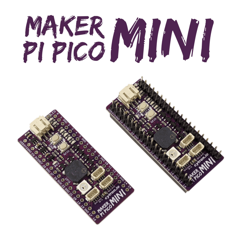
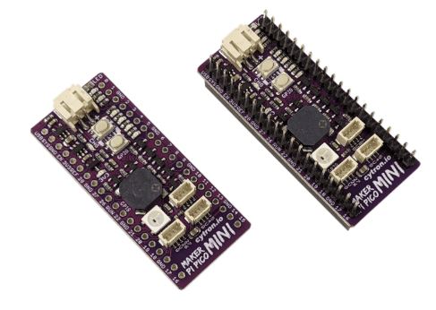
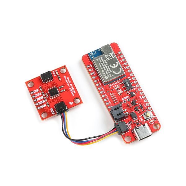
Cytron Technologies, a Malaysian company that specializes in designing boards and modules that help to simplify digital-making processes for makers and developers, has designed a Maker Pi PICO Mini Board aimed at simplifying projects with the Raspberry Pi Pico / Pico W.
Nicknamed “Small but Mighty”, the Maker Pi Pico Mini is designed for portability and can be powered by a LiPo connector, rechargeable via a USB port, and with an over-charge/over-discharge protection circuit. It is just like the $12 Maker Pi Pico board, just that it comes in a much more compact form and can fit into any project.
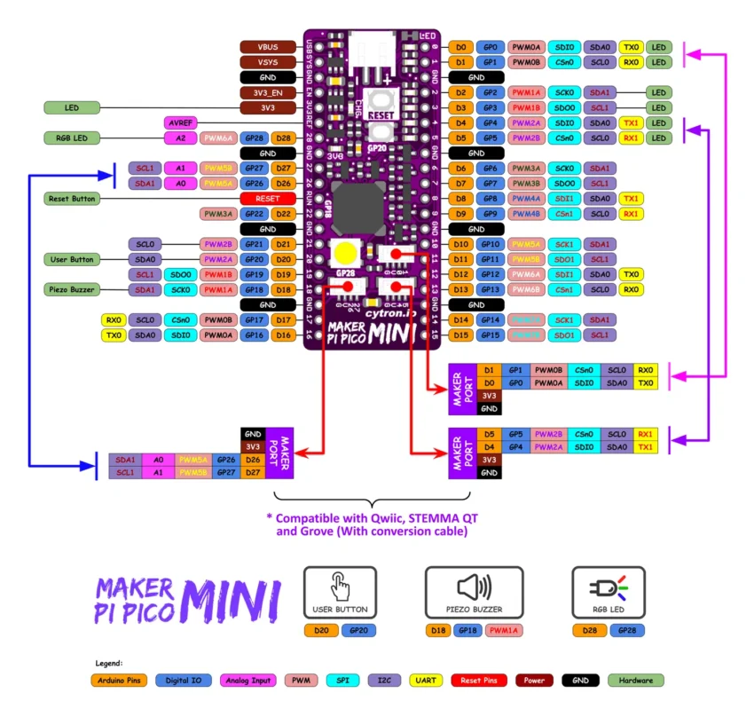
The Mini board is powered by the Raspberry Pi Pico/Pico W and comes equipped with plenty of useful features such as GPIO status LEDs, WS2812B Neopixel RGB LED, a passive piezo buzzer, a reset, and a user-programmable button.
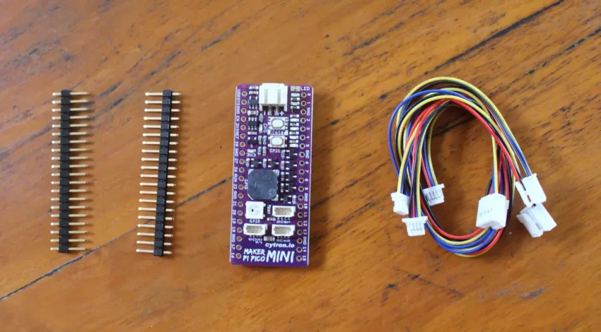
The board is so small that Cytron said it had to ditch the Grove connectors and replace them with three maker ports for expansion.
“Utilizing the JST-SH 4-way connector, Maker port is compatible with Sparkfun’s Qwiic modules and Adafruit’s STEMMA QT modules,” Cytron explains. “Qwiic and STEMMA QT are using I2C communications and can be daisy-chained. By using the included JST-ST to Grove conversion cables, Maker port is compatible with SeeedStudio’s Grove modules too. Besides I2C, Maker Port also supports UART, Analog input and Digital Input/Output.”
Specifications
Powered by RPi Pico / Pico W
1x Passive piezo buzzer
3X maker ports compatible with Qwiic, STEMMA QT, and Grove
2x 20-pin 2.54 mm pitch header on RPi Pico board with 26x GPIOs, 3x ADC, 2x I2C, 2x SPI, 16x PWM, 2x Programmable I/O blocks.
1x RGB LED (WS2812B Neopixel)
6x Status indicator LEDs for GPIO
Reset button and User programmable button (1x each)
Power: 5V via the micro USB port on the Raspberry Pi Pico W board; 2-pin connector for single-cell LiPo connector with overcharge/over discharge circuit.
Dimensions: 53.85 mm x 23.12 mm
OS Support: Arduino IDE, CircuitPython and MicroPython
Software Support
The Maker Pi PICO Mini board supports multiple programming languages that come with massive library support and examples to get you started with building your application in no time, whether for learning purposes or for building projects. These include Arduino, MicroPython, or CircuitPython
Further Details
More Information on the Maker Pi PICO Mini board, including links to its datasheet, pinout diagram, and getting started page can all be found on Cytron’s online store where the board sells for $8.90 to $14.40 depending on options. The option that comes without a Raspberry Pi Pico/Pico W sells for $8.90 while the pre-soldered RPi Pico variant of the board sells for $11.90 and the pre-soldered RPi Pico W (Wireless) goes for $14.40, both of which is preloaded with Circuit Python.
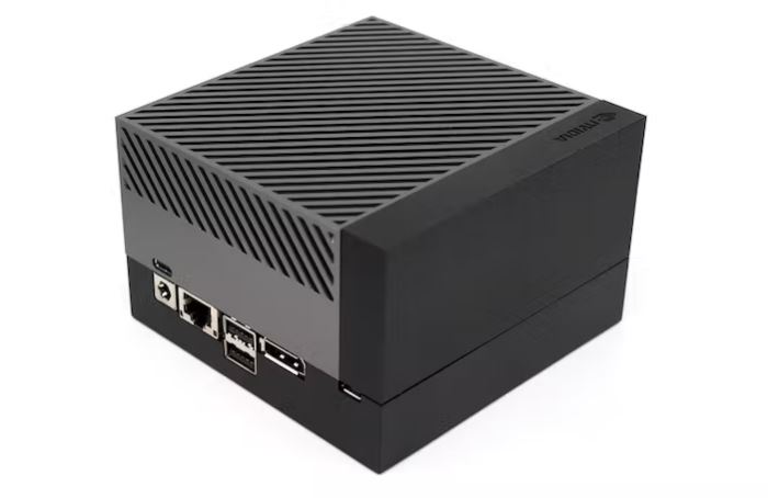
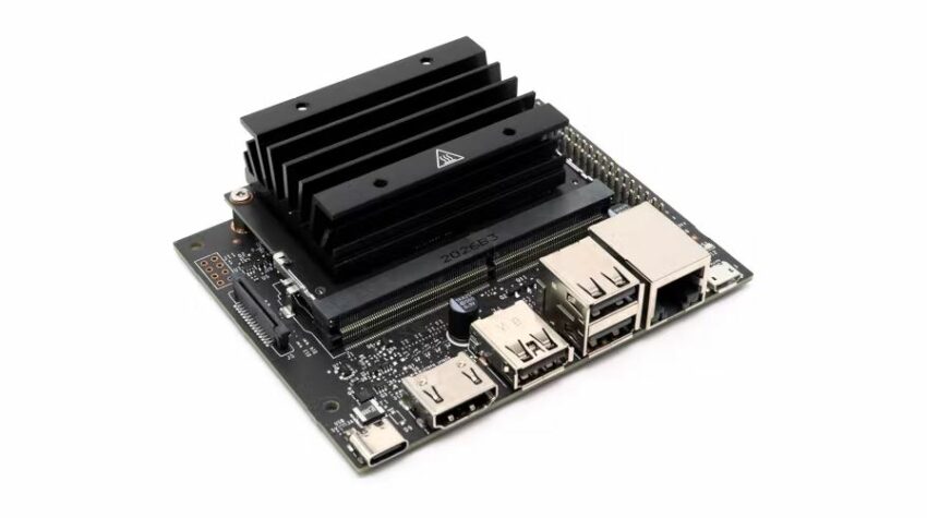
NVIDIA has released the CUDA Toolkit 11.8, the most recent version of the general-purpose graphics processing unit software. The latest CUDA Toolkit brings a big usability improvement for Jetson owners. It is equipped with new hardware capabilities which aim at speeding up CUDA applications and improving the programming model.
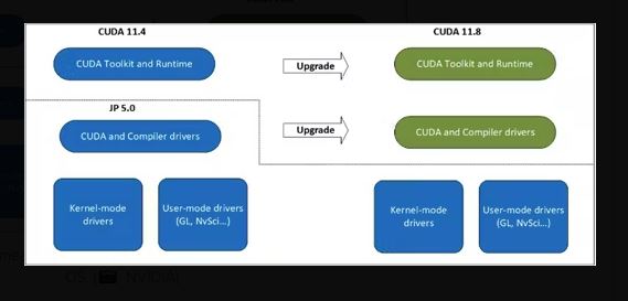
The CUDA Toolkit 11.8 release guarantees simpler and faster upgrades for customers working in the company’s embedded hardware ecosystem. It comes with a compatibility package that makes it easier to upgrade CUDA versions without having to utterly refresh the entire operating system.
“Starting from CUDA 11.8, [NVIDIA] has introduced an upgrade path that provides Jetson developers with an option to update the CUDA driver and the CUDA Toolkit to the latest versions. These upgrades are made possible by the introduction of the CUDA driver upgrade (also referred to as the CUDA compatibility package). Without this package, you were previously limited to the functionality provided by the default CUDA driver that was packaged in the Jetson Linux BSP (Board Support Package). You had no mechanism to upgrade to the latest CUDA driver and toolkit,”
the company explains.
A staff at NVIDIA also hinted that simplifying CUDA upgrades for NVIDIA Jetson users is only the tip of the iceberg as the company is working towards a time when Jetson developers will be able to just migrate to newer versions of the compute libraries without necessarily upgrading Jetson Linux.
“a future where Jetson developers can migrate to newer versions of the compute libraries without upgrading Jetson Linux. This CUDA feature that enables upgrading CUDA is a step in that direction.”
The CUDA Toolkit 11.8 version also comes with other crucial enhancements such as:
Support for lazy loading of CPU-side modules. This means functions and libraries will load faster on the CPU side along with reasonable memory footprint reductions, which will thereafter reduce the overall latency.
Improved multi-process service (MPS) signal handling – allows you to halt and terminate programs running in MPS environments without affecting other running processes.
Enhanced versions of the CUDA developer tools (such as Nsight Compute and Nsight Systems profiling tools) which help to identify and correct performance issues,
Support for next-generational NVIDIA Hopper and NVIDIA Ada Lovelace architecture processor. And,
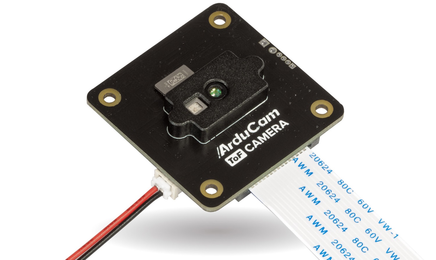
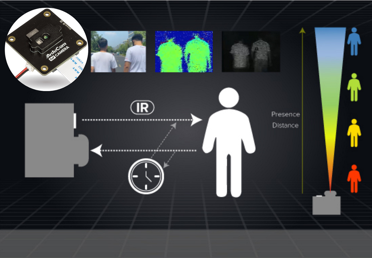
ArduCam is back with yet another camera module for Raspberry Pi with an active Time-of-Flight (ToF) sensor for an enhanced 3D Imaging experience. ArduCam’s new ToF camera for Raspberry Pi is now open for crowdfunding on Kickstart with a discounted price of $29.99, and a planned retail price of $50.
The ToF camera module uses a Vertical-Cavity Surface-Emitting Laser (VCSEL) operating at 940nm wavelength. The wavelength being greater than the visible spectrum wavelength, the camera module is prone to interference due to ambient light. Thus, making it suitable for indoor as well as outdoor applications.
The VCSEL, combined with a 240×180-resolution image sensor, offers a frame rate of 30fps on the Raspberry Pi. The camera module has a diagonal field of view (FOV) of 70°, and can capture depth data up to 2m in “near mode” and 4m in “far mode.” The camera module achieves this by changing the modulation frequency to either 75MHz or 37.5MHz.
The board comes in a small form factor of 38mm x 38mm and low power consumption of 3.5W. Due to its low power requirements, the camera module can be powered through the 5V GPIO supply of the Raspberry Pi as well.
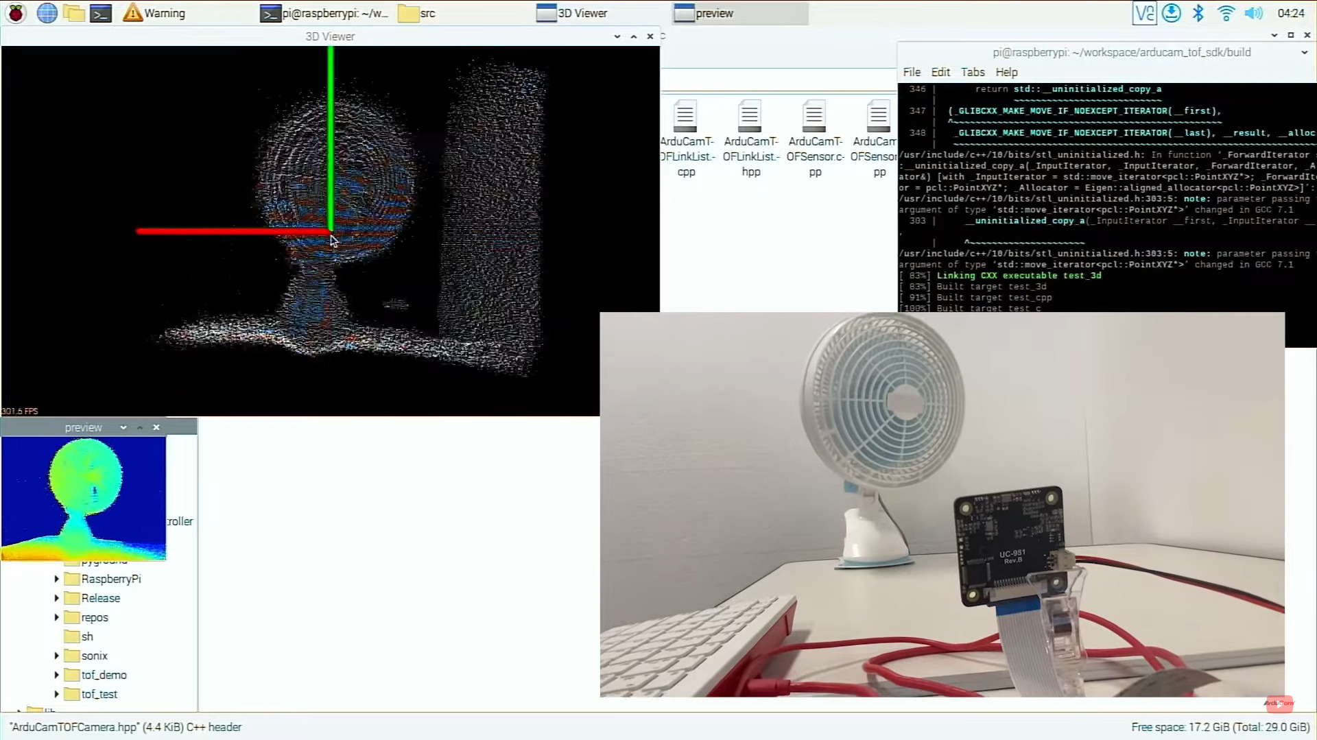
The ToF camera module can be easily interfaced with Raspberry Pi through the MIPI Camera Serial Interface (CSI) port. The Bullseye (32/64 bits) Raspberry Pi OS or any later releases support the integration of the camera module. The camera can be used with a wide range of machine vision libraries (like OpenCV, TensorFlow, etc.) as it can function as a standard V4L2 device as well, with support to C, C++, and Python.
Enhancing 3D Imaging with the ArduCam ToF Camera Module
The ToF camera module has numerous use cases including point cloud mapping, 3D photogrammetric, 3D depth analysis, and a lot more. ArduCam is trying to make the board suitable for Nvidia’s Jetson Nano/NX as well. With its low cost, low power requirements, and easy connectivity, the ToF camera module is ideal for various applications in a wide range of sectors including healthcare, surveillance, and robotics. You can support by funding on Kickstarter or apply for a free sample on ArduCam’s website.
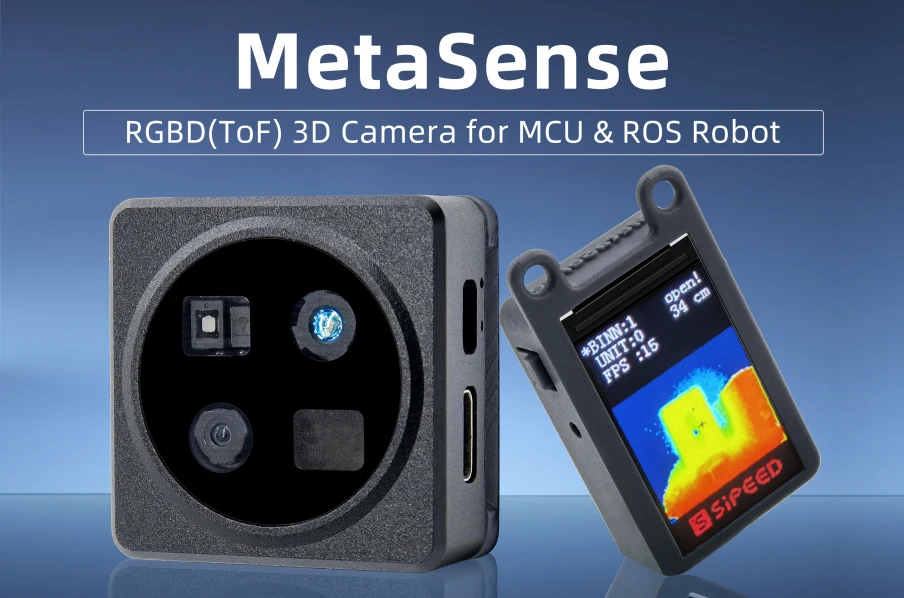
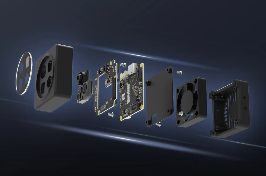
The Sipeed announced the MetaSense RGBD ToF family of 3D Cameras for microcontrollers and ROS-operated Robots, which is currently in development. The MetaSense 3D cameras use the Time-of-Flight (ToF) principle for providing 3-dimensional information. ToF utilizes light and measures the distance between objects based on the time taken by the light pulses to reflect back by the object.
MetaSense announced the development of two ToF Cameras – A075V, and A010. These cameras provide the coordinates in XYZ-axis, enabling the users to form a point cloud.
The A075V has a higher resolution of 320×240 as compared to the A010 with a resolution of 100×100. Moreover, the A075V has additional an RGB sensor and an Inertial Measurement Unit (IMU). The RGB sensor enables A075V to create colorful point clouds that can be used in applications like 3D scanning and 3D sense reconstruction.
It also features a powerful CPU along with an NPU (Neural Processing Unit) for processing complex data. Users can conveniently access the processed data just through a USB cable. The A010 is cheaper than A075V, making it ideal for beginners. It can be configured to different resolutions like 100×100, 50×50, or 25×25 depending on the microcontrollers used. Both the 3D cameras support integration with ROS1 and ROS2.
Technical Specifications of the MetaSense ToF Cameras
MetaSense A075V:
Dimensions: 36x36x23.5 mm
128MB RAM, 128MB ROM
Cortex A7 processor (1.5GHz) with 0.4T NPU
UART and USB2.0 ports
Distance measurement range : 0.2-2.0 m
MetaSense A010:
Dimensions: 23.25×40.70×10.50 mm
132KB RAM, 192KB ROM
32-bit RISC-V processor (144MHz)
UART and USB2.0 ports
Distance measurement range: 0.2-2.5m
Enhancing Computer Vision with the MetaSense 3D Cameras:
The new MetaSense ToF 3D cameras provide a 3D sense of the environment making them ideal for point cloud operations and other machine vision applications. Various use cases where these cameras can be used include autonomous navigation robots, obstacle avoidance, face recognition, passenger flow statistics, and a lot more. Moreover, MetaSense also offers Python SDKs that enable the users to view the 3D depth data on web browsers or ROS. The ToF 3D cameras are still in the prototyping phase and are open for crowdfunding. More information can be found in the Sipeeddocumentation.
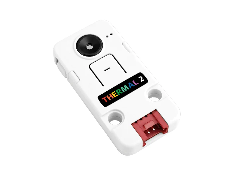
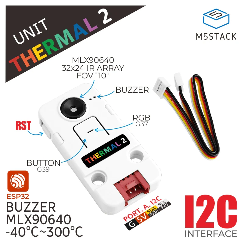
M5Stack embedded developers have developed the Thermal2 Unit thermal imaging camera. This is a newer version of the earlier Thermal Unit developed by the same company. The Melexis MLX90640 FIR thermal sensor used in the module is the core component. It has a wide range of temperature measurement abilities starting from as low as -40 deg C, and it can reach up to 300 deg C. It can also withstand an operating temperature in the range of -10 deg C to 60 deg C.
The sensor has a resolution of 32 x 24 px which offers 768 individual measurement points. The device has a 110×75 deg field view and a refresh rate from 0.5Hz up to 64Hz. The refresh rate is programmable as well. The power consumption is only 2.5W, operating at 5V with a current consumption of 500mA.
The MCU used in the device is the ESP32-PICO-D4, with many features included, such as a flash memory of 4 MB, Bluetooth 4.2 radio, and SRAM of 520kB. It is also integrated with two low-power Xtensa LX6 32-bit microcontroller cores, two banks of 8kB in RTC, and 2.4GHz 802.11b/g/n Wi-Fi.
It is a very lightweight module weighing merely 4.9g with a small size of 48mm x 24mm x 8mm. To make the module ready to use, a user-addressable RGB LED and a button is attached. The device can operate in standalone or I2C mode, and a default firmware is already flashed in the module. However, UIFlow or Arduino IDE can be used to program the device, as confirmed by the makers.
Some prominent applications where it can be used are motion detection and visual infrared thermometer. It can also be used for non-contact temperature measurements with high precision. The applications are of course extended to any DIY projects as well. The Thermal2 is now available at a price of $69.90 for purchase at the M5STack Store. A separate cable is not necessary, as an HY2.0-4P cable comes bundled with it.
The Demultiplexer or DEMUX is a combinational logic circuit that connects one input line to one of the several output lines, one at a time. Like a Multiplexer, the Demultiplexer contains no memory, storage, or feedback. Being a combinational logic circuit, its output is solely dependent on the information present on its input lines. Demultiplexing refers to the reverse of the Multiplexing process. As discussed in the previous article, the Multiplexer combines several input lines into a single channel or output line for sending information or data which may be either analog or digital. The reverse of Multiplexing is to combine several output lines into a single channel connecting to an input line. For a multiplexer, there is more than one (1) input and only ONE output. Whereas, for a Demultiplexer, there is only ONE input and several output lines.
The input line is routed or switched to output lines one at a time by the application of a control line(s). Similar to the multiplexers, the demultiplexers are like mechanical rotary switches which select one of the output lines or channels to be switched to the common input.
The Demultiplexers are also classified into Analogue and Digital categories. The Multiplexers and Demultiplexers are used in pairs and should match their construction, signal-handling capabilities, etc.
The selection of output lines in demultiplexers is controlled using separate input lines which are referred to as “Select Lines”. The logical combination of these Select Lines helps in selecting one of the output lines. For example, a logical “LOW” at the select line means to select Output Line-0, and a logical “HIGH” to select Output Line-1. The data output lines are normally in even numbers and are given by 2n. Whereas, the “n” corresponds to the number of control inputs required for the selection of data output lines.
Demultiplexer Symbol
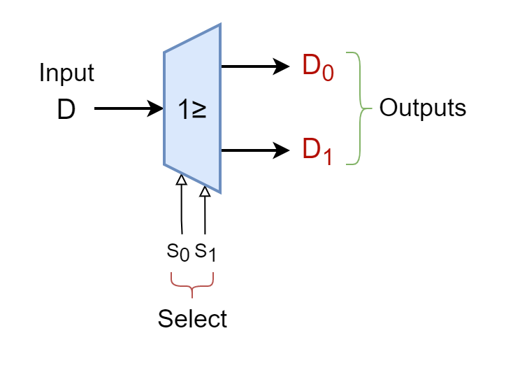
In the following figure, a Demultiplexer symbol has been shown. It is the simplest one-to-two (1-to-2) Demultiplexer.
Figure 1: The Demultiplexer
1-to-2 Demultiplexer
In the following figure, a 1-to-2 Demultiplexer has been shown along with its truth table.
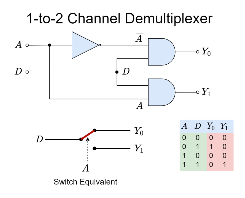
Figure 2: The 1-to-2 Demultiplexer
The above 1-to-2 Demultiplexer is constructed using basic logic gates. The data input line is D and the output lines are Y0, & Y1. The Select or Control Line is indicated by input A. From the logic diagram and given Truth Table, it is obvious that when Select Input “A” is “LOW” or “0” then Output Line “Y0” gets selected as an output. The signals present on input pass through the logic circuit and appear at output “Y0”. Whilst, the Output Line “Y1” gets blocked when Select Line “A” is set to “LOW”. The output selection phenomena get reversed when Select Line “A” is set to “HIGH” or “1” i.e. the Output Line “Y1” connects with the input “D” and Data Output “Y0” gets blocked.
By simply setting the Select Line “A” to “LOW” or “HIGH” logic, the input line can be switched to the outputs depending on the logic level of “A”. The given circuit is acting as a Single-Pole-Double-Through (SPDT) switch. As discussed above, with only one (1) Select line i.e. n=1, the input line can be switched to a total of two (2n = 21 = 2) output lines. The described circuit is the simplest form of a Demultiplexer which is a 1-to-2 Demultiplexer.
The 1-to-2 Demultiplexer is the simplest or basic form of a Demultiplexer which has only one (1) input and two (2) outputs. In order to increase the number of outputs of a Demultiplexer, a 1-to-2 Demultiplexer can be used as a basic building block for the construction of higher-output Demultiplexers. As mentioned above, the number of outputs of a Demultiplexer will be in even numbers so the next stage after two (2) output-Demultiplexer is a four (4) output-Demultiplexer. For a four (4) output Demultiplexer, a total of two (n = 2) Select Lines are required.
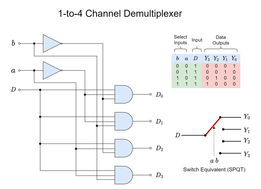
1-to-4 Demultiplexer
In the following figure, a 1-to-4 Demultiplexer has been shown along with its Truth Table.
Figure 3: The 1-to-4 Demultiplexer along with Truth Table and Switch Analogy
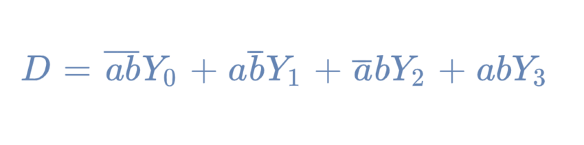
In the above 1-to-4 Demultiplexer, the Output Lines are Y0, Y1, Y2, and Y3 and the Select Lines are “a”, and “b”. The Boolean expression of the above-given 1-to-4 Demultiplexer is:
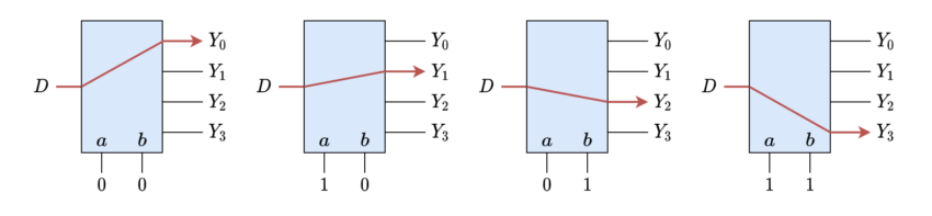
The 1-to-4 Demultiplexer circuit acts as a Single-Pole-Quad-Through (SPQT) switch. At any instant, only one of the four outputs will be connected to the input “D” whilst others remain blocked depending on the logic conditions of Select Lines “a” and “b”. For example, in order to connect the Data Input “D” to the Output Line “Y2”, the logic states required are “A=0” and “B=1”. Likewise, other Data Output selections can be made by setting the logic states of Select Lines, accordingly. The selection of Output Lines against the logic states of Select Lines is shown in the following figure.
Figure 4: The logic states of Select Lines and Switching Positions
The output lines of a Demultiplexer can be further increased to 8, 16, … etc. by increasing the select lines to 3, 4, … etc., respectively.
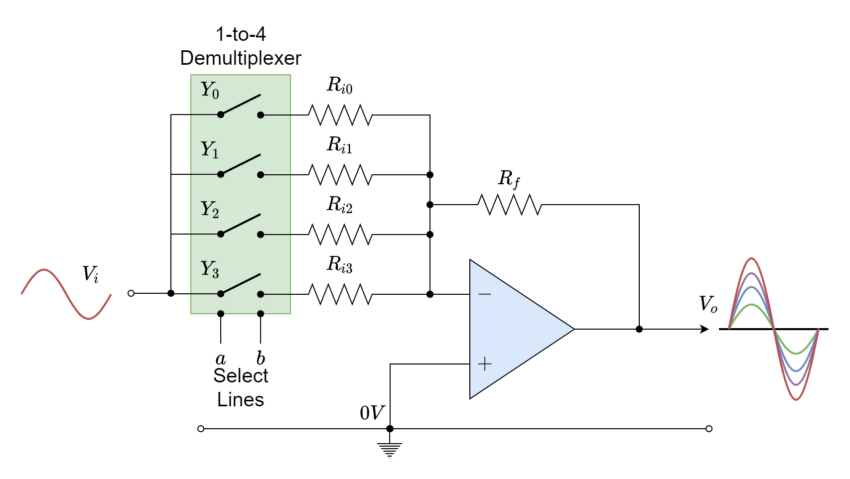
Adjustable Amplifier Gain Application
In the Multiplexer article, an adjustable gain amplifier was constructed using a multiplexer in the feedback. The same can be achieved by using a Demultiplexer but instead of using it in the feedback, it is placed at the input of the amplifier circuit. In the following figure, an adjustable inverting operational amplifier has been shown with multiple input paths depending on the amplification required.
Figure 5: The multiple channel gain amplifier using Demultiplexer
The placement of the Demultiplexer at the input is obvious as it essentially converts a single input to multiple paths. Each path has been set to present a different input resistance which ultimately sets the gain of the amplifier. The gain of the amplifier is mainly dependent on input and feedback resistances. However, in the above configuration, the gain is adjustable using only input resistance as the feedback resistance is fixed. The gain of the input signal (audio) will be set as per Select Lines which are setting the input resistance of the op-amp.
The Demultiplexers are used in the reception of single-input data to distribute over multiple channels, buses, or transmission lines such as in Digital Systems, LAN or Ethernet Switches, etc.
The Demultiplexers are commonly available in commercial I.C. packages such as in TTL: 74LS15138 (Single 1-to-8), and 74LS139 (Dual 1-to-4) or in CMOS: CD4514 (Single 1-16) Demultiplexers, etc. The number of inputs of a Demultiplexer can be increased by cascading the aforementioned TTL or CMOS devices. Most of the commercial I.C. packages come with Enable pin which enables or disables the operation of Demultiplexing.
Conclusion
A Demultiplexer is a combinational logic circuit with the ability to switch a single input line to one of several output lines.
Being a combinational logic circuit, the Demultiplexer’s output is dependent on the state of inputs only and, as such, uses no memory, storage, or a feedback path.
The selection of individual output lines is made through the “Select” or “Control” line(s). The number of “Select” or “Control” lines yields the number of Output Lines that can be controlled i.e. 2n. Where “n” represents the number of “Select” or “Control” lines. For example, in a Demultiplexer with two (n=2) Select Lines, a total of four (2n = 22 = 4) Output Lines can be switched to the common Data Input Line. Because of this, the number of Output Lines is in even numbers.
The digital Demultiplexers are used for the reception of serial data over a single line to distribute over multiple channels, buses, etc. The analog demultiplexers are commonly used in the pre-amplification of audio, and video signals.
The Demultiplexers are commercially available in form of I.C. packages such as 74LS15138 (Single 1-to-8), 74LS139 (Dual 1-to-4), and CD4514, etc.
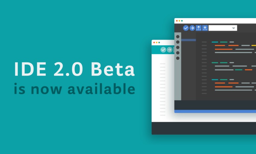
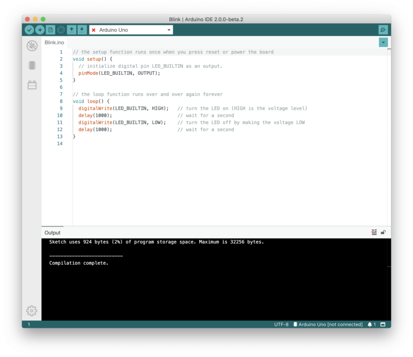
Arduino has now declared the Arduino IDE 2.0 ready for primetime use, effectively ending the era of the previous Arduino IDE. The Arduino team stated that moving it from the beta version to the general release was a result of the feedback they received from the Arduino community which has helped them focus on what is more meaningful to the wildest user base.
“The enormous amount of user feedback allowed us to identify the weakest spots such as code assist and completion, serial output, loading, and compilation time. We made it all better now,” the team said. “A special mention goes out to Paul Stoffregen who has provided enormous feedback to the IDE development team and has been actively developing the initial support for advanced third-party platforms such as Teensy for IDE 2.0 (currently experimental).”
The latest release version is indeed a big step up from the previous release. It is faster, more powerful, and boasts plenty of new features to help you to develop your code more easily. A big shift towards better usability I must say.
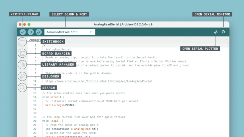
The new version provides a more modern editor, an improved user interface, autocomplete during coding, navigation shortcuts, integrated support for storing sketches in the Arduino Cloud, the ability to quickly switch to and from a dark mode theme, and the ability to run the revamped serial plotter alongside the serial monitor. There’s also a new sidebar to make the most commonly used tools more accessible and a debugger with powerful features like Breakpoints, Step-into, and Step-Over, which help you really understand what your code is doing.
The Arduino team assured users that the new IDE comes with a lot of likable features, though it might take a while to discover and use all the new features effectively.
“Some of them are carry-overs from the “Arduino Pro IDE” that we covered a few years ago, but it’s great to see the software evolve and improve over time. Installation is straightforward, and will automatically pull in any libraries and sketches that you created in previous versions of the Arduino software to ease the transition.”
The latest release can also check for, download, and install updates to the IDE itself without having to manually open a web browser and download the latest installer.
Further details on the stable Arduino IDE 2.0
Download options for Windows, Linux, and macOS, alongside other details, can be found on the software page of the company’s official website while the IDE’s source codes and a support link in case you need any assistance are also available on GitHub.
Colorado-based embedded electronics manufacturer, SparkFun, is back with another exciting development board in the same form factor as the Adafruit Feather boards. The SparkFun Thing Plus DA16200 development board has an integrated ultra-low power Wi-Fi system-on-chip. The Wi-Fi SoC from dialog enables users to create next-gen Wi-Fi and IoT applications with ease. Depending on the application, such low power consumption can increase battery life by up to a year or more while being able to be deployed in space-constrained use cases.
The new SparkFun Thing Plus DA16200 development board is powered by an Arm Cortex-M4F microcontroller core with a clock speed of up to 150MHz. On a single silicon chip, the module houses a 2.4GHz IEEE802.11b/g/n Wi-Fi connectivity together with a baseband processor, media access controller (MAC), on-chip memory, and a host networking application processor. An external network processor, CPU, or microcontroller is not necessary because the system-on-chip (SoC) has full offload capabilities to operate the entire networking OS and TCP/IP stack on the chip. Thanks to its numerous sleep modes, which let you use current draws between 0.2 and 3.5 A, the DA16200 is a great choice for your next Internet of Things project.
SparkFun claims, “To make the Thing Plus as easy to use as possible, we’ve made the board Feather-compatible and it utilizes our handy Qwiic Connect System which means no soldering or shields are required to connect it to the rest of your system!”
Despite its compact size, the SparkFun DA16200 Thing Plus offers up to four 12-bit analog-to-digital converter (ADC) channels, two UARTs, one SPI bus, and one I2C bus on its 16 multifunctional GPIO pins. The board can be easily mounted on a breadboard due to its convenient design. It also features a four-pin Qwiic connector and a two-pin JST connector for an external LiPo battery that can be charged with the onboard USB type-C port.
The hardware is also capable of Wi-Fi Direct and comes with WPS certification from the Wi-Fi Alliance. Wi-Fi Certifications can be transferred in accordance with the Wi-Fi Alliance transfer rules without retesting. DA16200 with its wide range of communication peripherals, connectivity, and low power consumption makes it an ideal choice for numerous IoT applications including home automation, security devices, surveillance, and a lot more.
The ultra-low power SparkFun Thing Plus DA16200 development board is priced at $34.95, which can be ordered from the official product page. The manufacturer has also provided a hookup guide on the website.
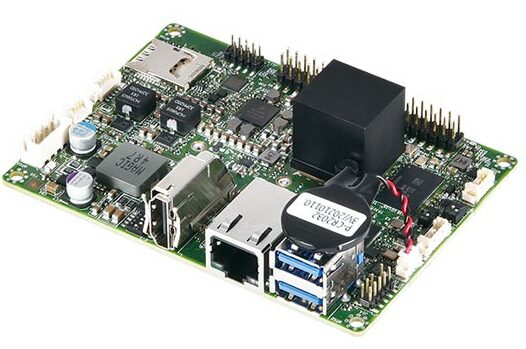
If you are looking for a form factor that is way smaller than the mini-ITX form (75% smaller), then you should be talking about the Pico-ITX form factor, developed in 2007 by VIA as part of its strategy to enable system developers and OEMs to create smaller, lighter and quieter devices than ever before. The Pico-ITX form factor has actually opened up a new world of possibilities for embedded IoT and we have seen it being widely adopted in a large variety of small-footprint systems and off-the-shelf platforms, one of which is the small and multifunctional ND118T board recently released by ICP.
The ND118T board is characterized by an ARM-based platform combined with rich feature sets, low power consumption, and high-processing power and performance. It comes equipped with a 1.3 GHz NXP I.MX8M Cortex A53 dual/quad-core system-on-chip coupled with up to 32GB of eMMC storage, one microSD card slot, one GbE LAN port, a customized LPDDR4 onboard memory with options (1GB, 2GB, 4GB), a Raspberry Pi fully compatible 40-pin GPIO header, a MiniPCIe socket, and a Gigabit RJ45 LAN port. It is a perfect choice for embedded applications that require low power consumption in an industrial environment.
The board also offers dual display support with full 4K UltraHD resolution and HDR video quality as well as professional audio output at its highest level.
1x USB 2.0 port header / 1x USB 2.0 OTG port header
I/O
1x 40-pin GPIO header fully compatible with Raspberry Pi 40-pin header
1x RS232 / 422 / 485
Expansion Slot
Mini PCIe (PCIe / USB)
Watchdog Timer
1x Watchdog timer
Power
DC-in 12V to 24V (4-pin power connector)
Dimension
100 mm x 72 mm or 3.9 x 2.8 in (Pico-ITX form factor)
Environment
Operating Temperature: -10°C to 65°C
Storage Temperature: -20°C to 70°C
Operating Humidity: 10% to 95% RH (non condensing)
OS Support
Android 9 Pie (Kernel version 4.14.9)
Yocto 3.2
Certification
CE/FCC
Pricing and Availability
The 1GB RAM version of the ND118T board sells for about 216€ (that’s around $210) while the 2GB RAM version goes for 240€ ($233) and the 4GB RAM for 304€ ($295) More useful details on the ND118 board can be found on the product page or the company’s announcement page. You may have to sign up to view the price list and complete the purchase.
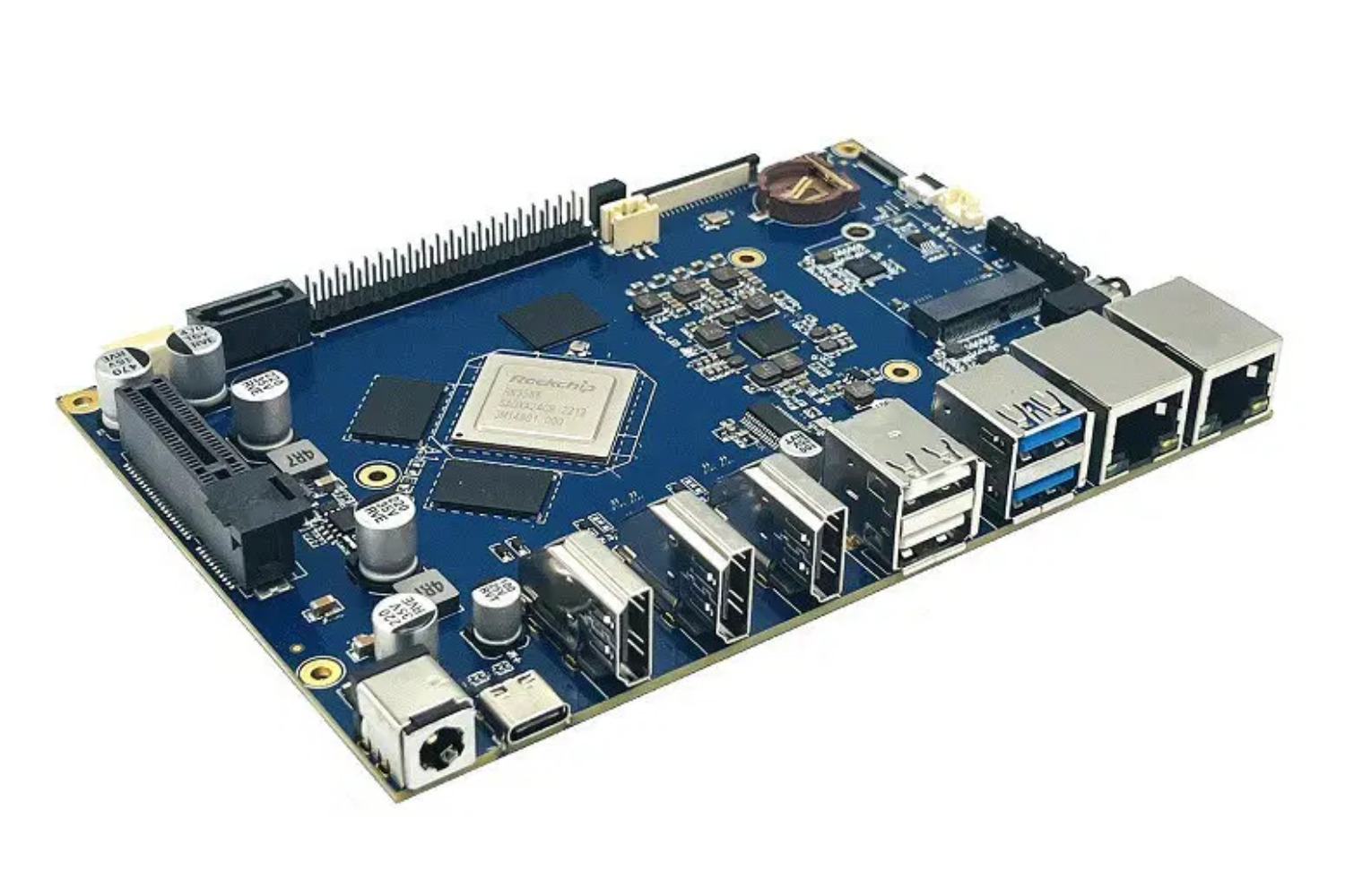
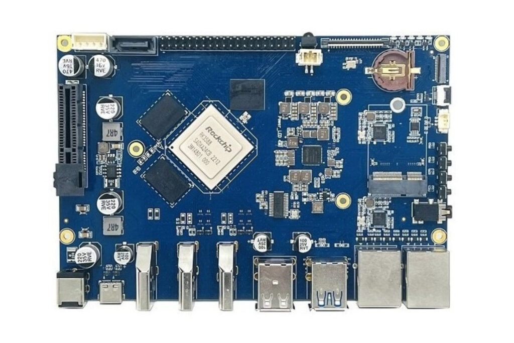
SinoVoip Co. Limited has introduced a Banana PiBPI-W3 router-based development board built around the Rockchip RK3588 system on a chip featuring a quad-core Arm Cortex-A76 processor and a quad-core Arm Cortex-A55 processor which makes it a total of eight core CPU processors. The hardware delivers 6 TOPs in the INT8 neural processing unit integrated with 8GB of memory and upgradeable 32GB eMMC storage to operate various open-source operating systems, such as OpenWrt, Android, and Linux.
Recently another hardware was seen integrated with RK3588, the Mixtile Blade 3, a stackable, high-performance single-board computer. The system-on-chip has an impressive graphics processing unit, Arm Mali-G610 MP4 that supports OpenGL ES 1.1/2.0/3.2, OpenCL 2.2, Vulkan 1.1 Embedded high-performance 2D acceleration hardware. Video capabilities are the key highlights of Rockchip RK3588, with 8K at 60 frames per second video decoding and 8K at 30 frames per second video encoding.
Specifications of Banana Pi BPI-W3 board:
SoC: Rockchip RK3588 system-on-chip
CPU: A quad-core Arm Cortex-A76 and a quad-core Arm Cortex-A55 processor core
GPU: Arm Mali-G610 MP4
NPU: 6 tera operations per second at INT8
Memory: 8GB LPDDR4
Storage: 32GB eMMC flash
Interface: 1x SATA hard disk interface, 2x 10/100/1000Mbps Ethernet
Video encode: Supports 8K at 30 frames per second, H.265 and H264 video encoding
Video decode: Supports 8K at 60 frames per second, H.265, AVS2 profile, VP9 video decoding
HDMI: 2x HDMI out and 1x HDMI in
GPIOs: 40x pins header, 28x GPIOs
Serial communication: UART, I2C, SPI, I2S
Software: Android 12.0 and Linux operating system
Power: 12V/2A
Operating temperature: 0°C to 80°C
Dimensions: 148×101 mm
Even though the hardware platform is equipped with 32GB eMMC flash storage, the manufacturer has provided the Banana Pi BPI-W3 single-board computer with a SATA interface for an external hard disk. Along with rich expansion headers and 28 general-purpose input/output pins, it makes the user want to interface with external I2C sensors for added capabilities.
On the software side, the user has an option between Android 12.0 and Linux operating systems. However, for video decoding and encoding applications, it is recommended to use Android 12.0 for better performance and optimization.
For more information on the product, Banana Pi has provided a wiki page.