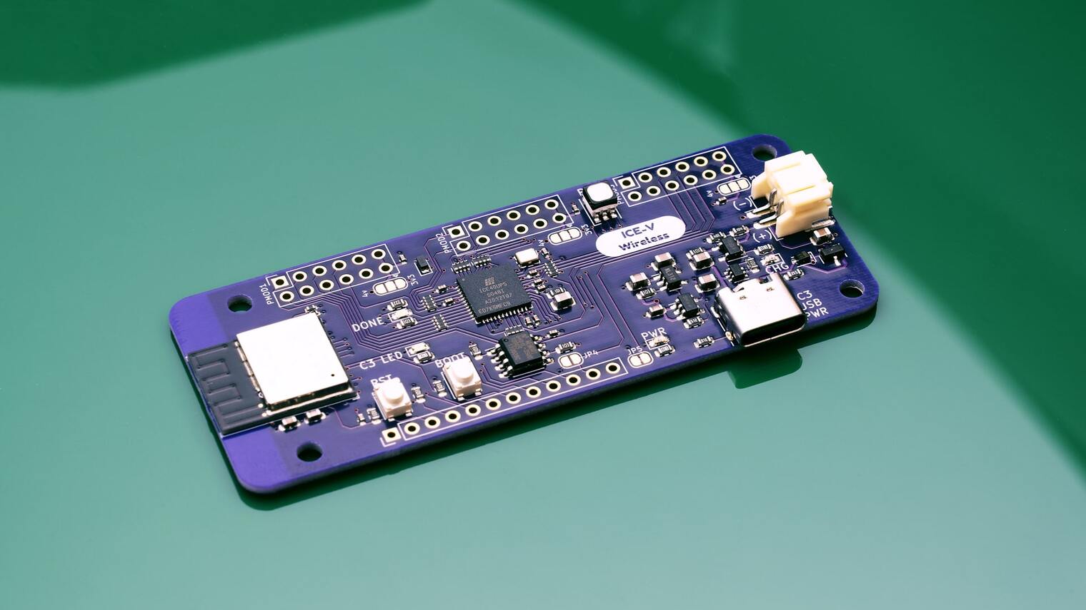
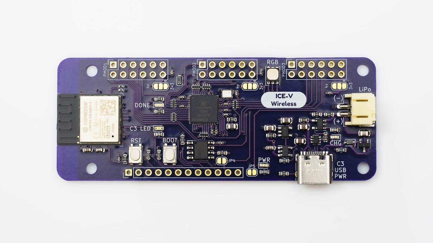
ICE-V wireless mini development board is currently active on GroupGets for community support, which features an ICE40UP5K FPGA and an ESP32-C3-MINI system on chip. The development board looks fairly similar to the Feather board, but there is no confirmation on the dimensions yet. The wireless interface driven by ESP32-C3 helps the hardware platform serve the growing demand for IoT use cases on an enterprise scale. The ESP32-C3 system-on-chip supports 2.4GHz Wi-Fi along with Bluetooth 5.0 powered by a RISC-V single-core microprocessor.
As mentioned earlier, the ICE-V wireless development board has the combined power of ICE40UP5K and ESP32-C3 SoC to deliver high computing performance in a small form factor. The interesting thing about ESP32-C3-MINI-1 is that it has an onboard PCB antenna. The general-purpose wireless connectivity module, ESP32-C3, has a rich set of peripherals making it an ideal choice for smart homes, industrial automation, healthcare, consumer electronics, etc.
Inside the ESP32-C3 system-on-chip is the ESP32-C3FN4 embedded 32-bit RISC-V single-core processor clocked up to a frequency of 160MHz and integrated 400kB memory and 384kB storage along with 4MB embedded flash. The key highlight of the SoC is the wireless connectivity, which includes support for Wi-Fi IEEE802.11b/g/n with simultaneous support for Infrastructure BSS in Station mode, SoftAP mode, Station + SoftAP mode, and promiscuous mode. Also comes Bluetooth Low Energy connectivity with speeds of 125 Kbps, 500 Kbps, 1 Mbps, 2 Mbps.
The other computing performance is delivered by the Lattice Semiconductor iCE40 ultra-low-power FPGA module for mobile applications, such as smartphones, tablets and hand-held devices. The flexible logic architecture features 5280 logic cells, offered in WLCS and QFN packages. The ultra-low power device has advanced 40nm low power process technology to deliver as low as 100µA standby current. The hardware includes integrated SPI and I2C blocks for interfacing with mobile sensors and application processors.
On the software side, the manufacturers, Qwerty Embedded Design, put out an update that the firmware development has been progressing well with over 65% funding reached. Eric, an engineer at Qwerty Embedded Design, was able to get the MicroPython port up and running on ESP32-C3 and has a script for flashing the FPGA. The GitHub repository has more details on the ICE-V-Micropython and how to get it working. If you are interested in supporting the project, head to the crowdfunding project page for more details.
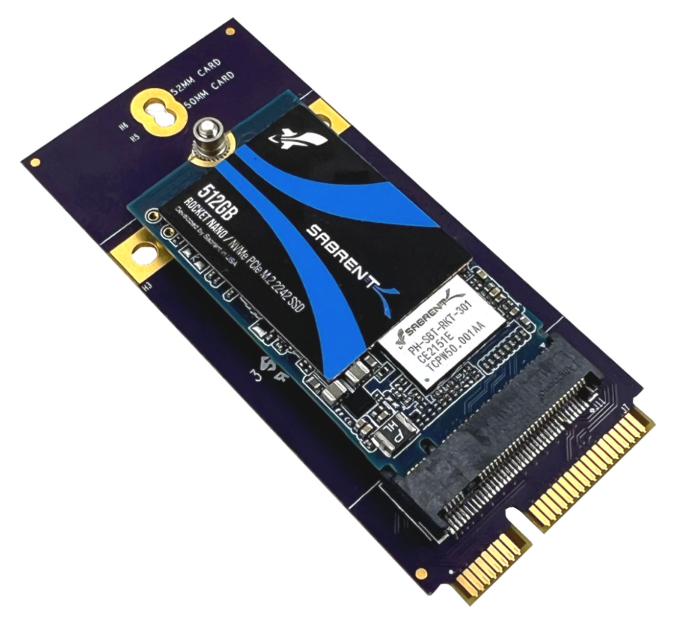
Gateworks is proud to announce the GW16148 Mini-PCIe to M.2 NVME storage adapter. It allows any of the Mini-PCIe slots with PCIe signalling on Gateworks SBCs to be used for a M.2 NVME storage drive. NVME allows for flash storage expansion that offers better performance than a microSD and provides an option when mSATA is not supported.
NVME is used widely in the consumer space, often featuring storage devices that are 80mm long and using 4x PCIe lanes built for desktop PCs. The Gateworks adapter allows for 1x PCIe lane with a maximum card length of 52mm. One of the ideal sizes for the GW16148 adapter is a 2242 form-factor. NVME drives are available from many different memory manufacturers and are not included with the Gateworks adapter.
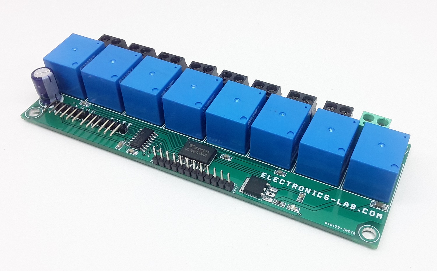
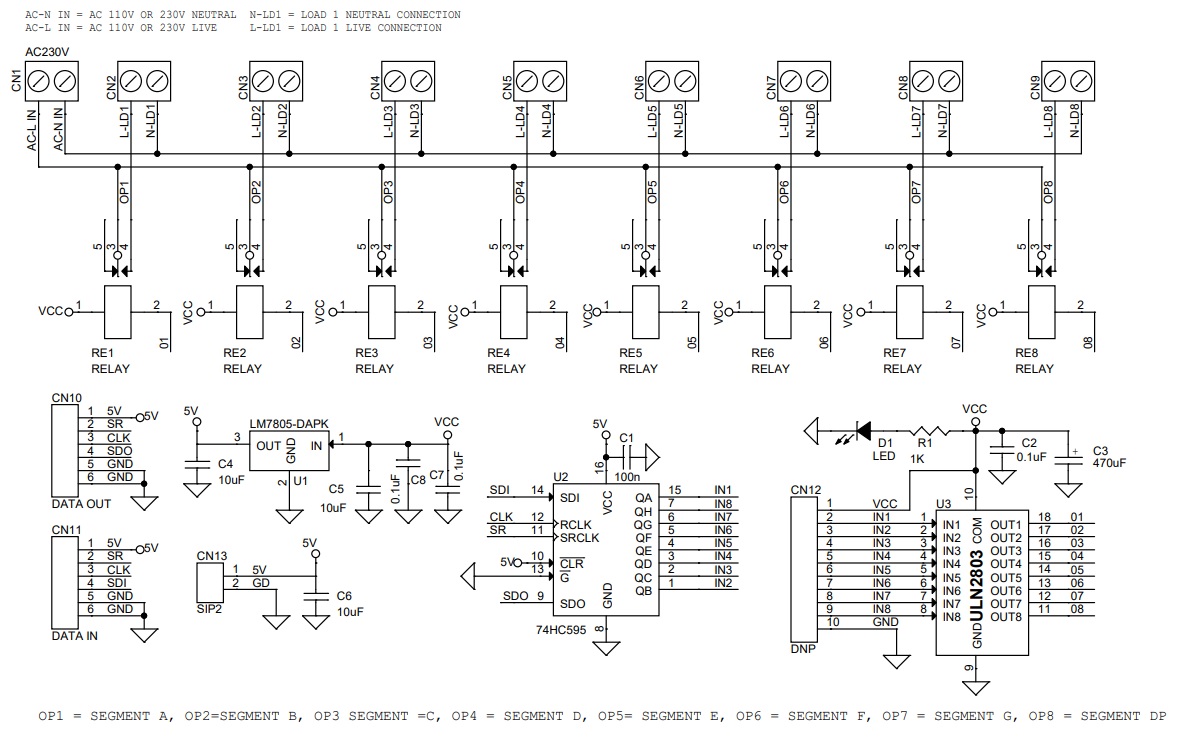
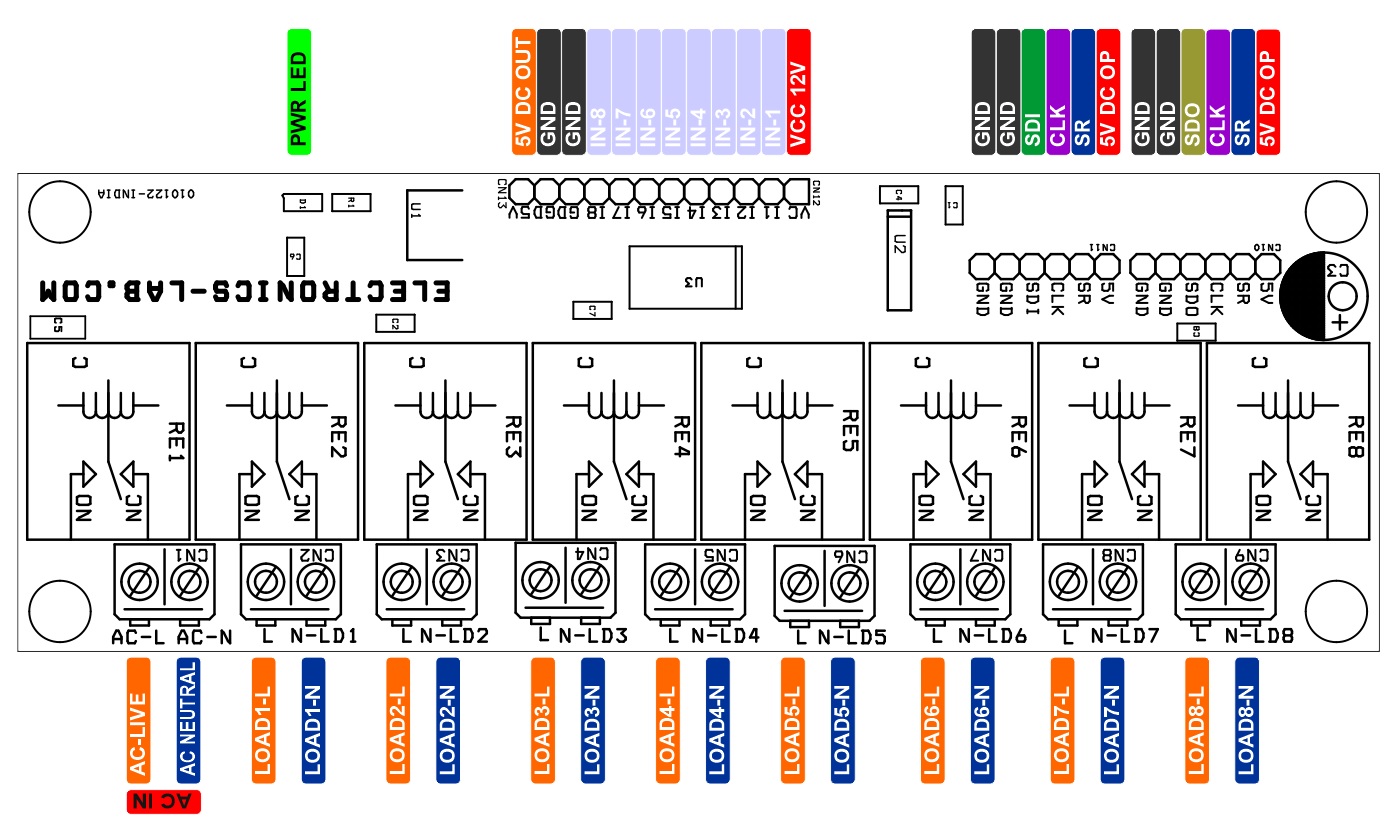
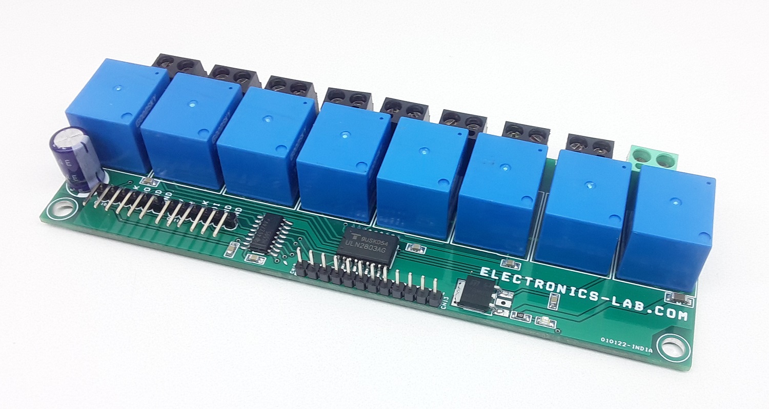
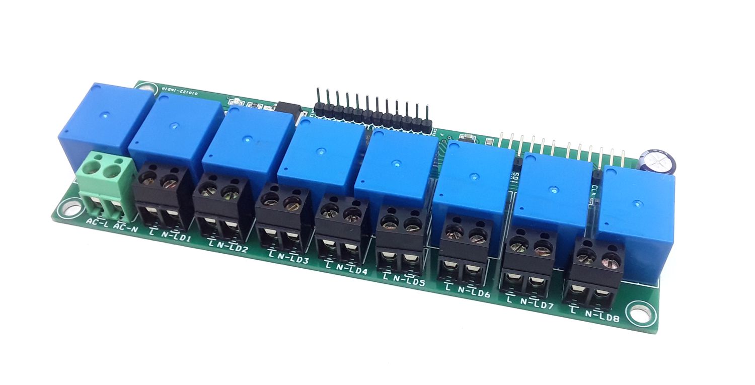
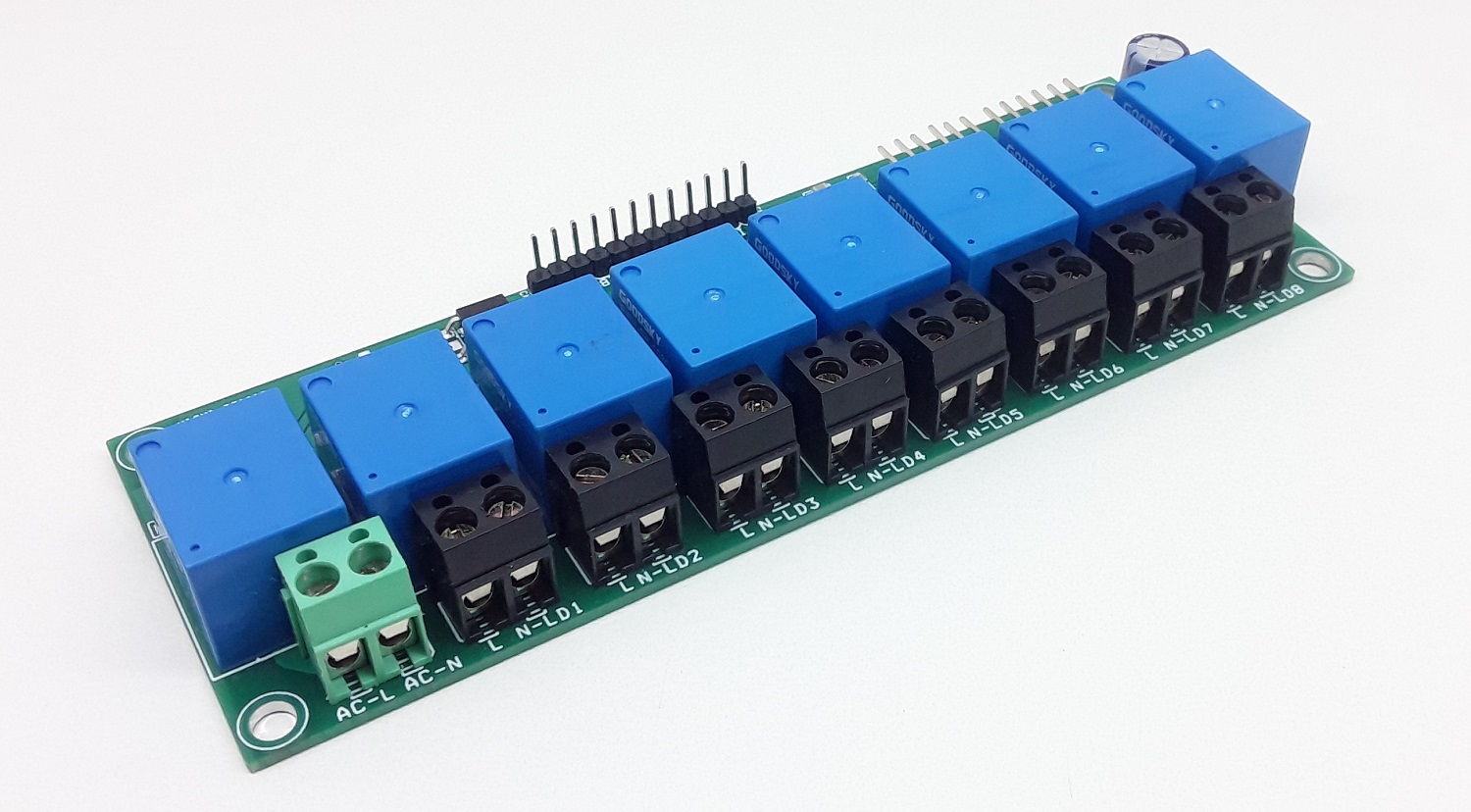
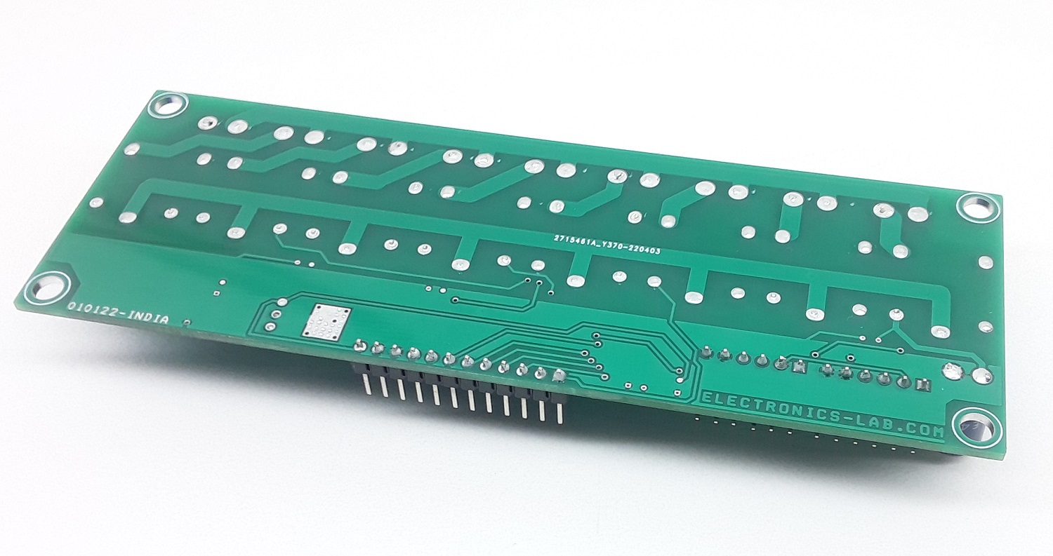
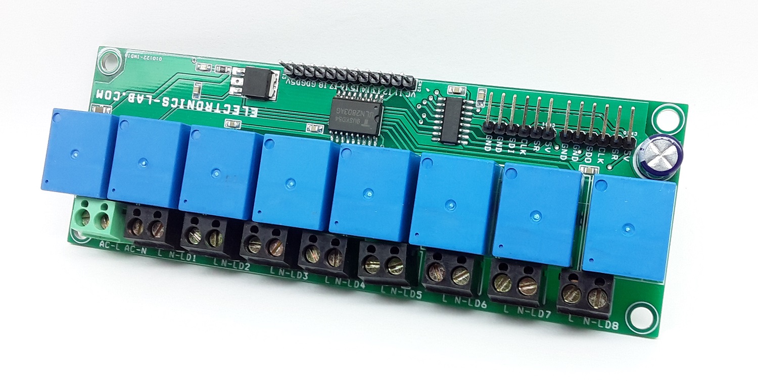
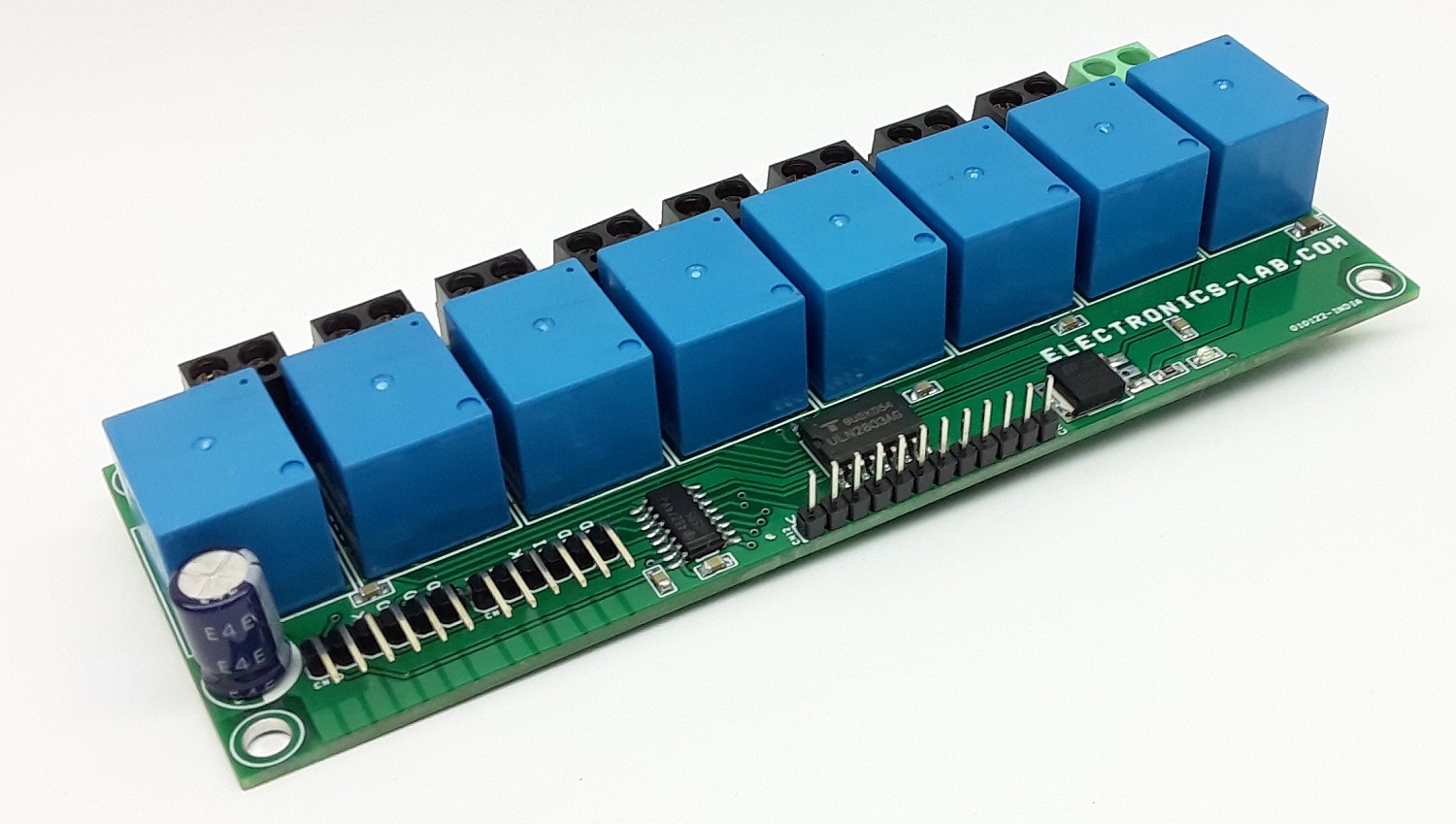
This is an SPI Interface multichannel relay board for high voltage AC or low voltage DC loads. It is ideal for controlling LEDs lights, coffee machines, fans, pumps, or other high-voltage electrical appliances. The board also breaks out the SPI header, so controlling other boards is still possible. Each relay can handle current up to 7A @ 250V AC/30V DC. This 8 x channel board is mainly designed for AC loads, but it can also drive DC loads, screw terminals on each channel enable the easy interface of the AC load, and each point is marked as AC-Live and AC Neutral. Refer to the connection diagram for the interface. The project consists of 8 x 12V relays with load capacity 7A @ 250V AC, ULN2803 8 channel relay driver, 74HC595 SPI to 8 output, 5V regulator 7805, power LED, screw terminals for loads and AC input, header connector for SPI input and output.
SPI Interface: 6-pin header CN11 is provided for data input and CN10 connector is the SPI output that can be interfaced with multiple boards.
Note1: This board also can be used with direct 8 channel TTL inputs by not installing the 74HC595 chip, use CN12 connector for 8 TTL inputs, IN1, 1N2,1N3,1N4, IN5, IN6, IN7, IN8
Note 2: Each relay can drive a load of up to 7 A, but it is not advisable to use full current as PCB tracks can not handle 7 A x 8 Channel = 56Amps. The maximum advisable load on each channel is 1.2A, the total load on each channel is 1.2A x 230V = 276W maximum.
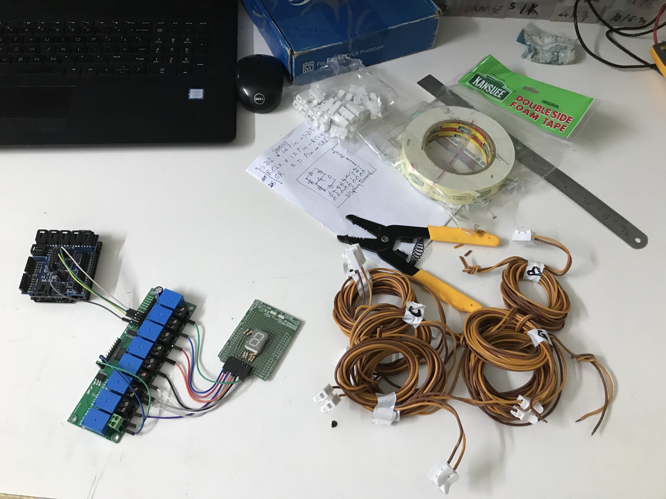
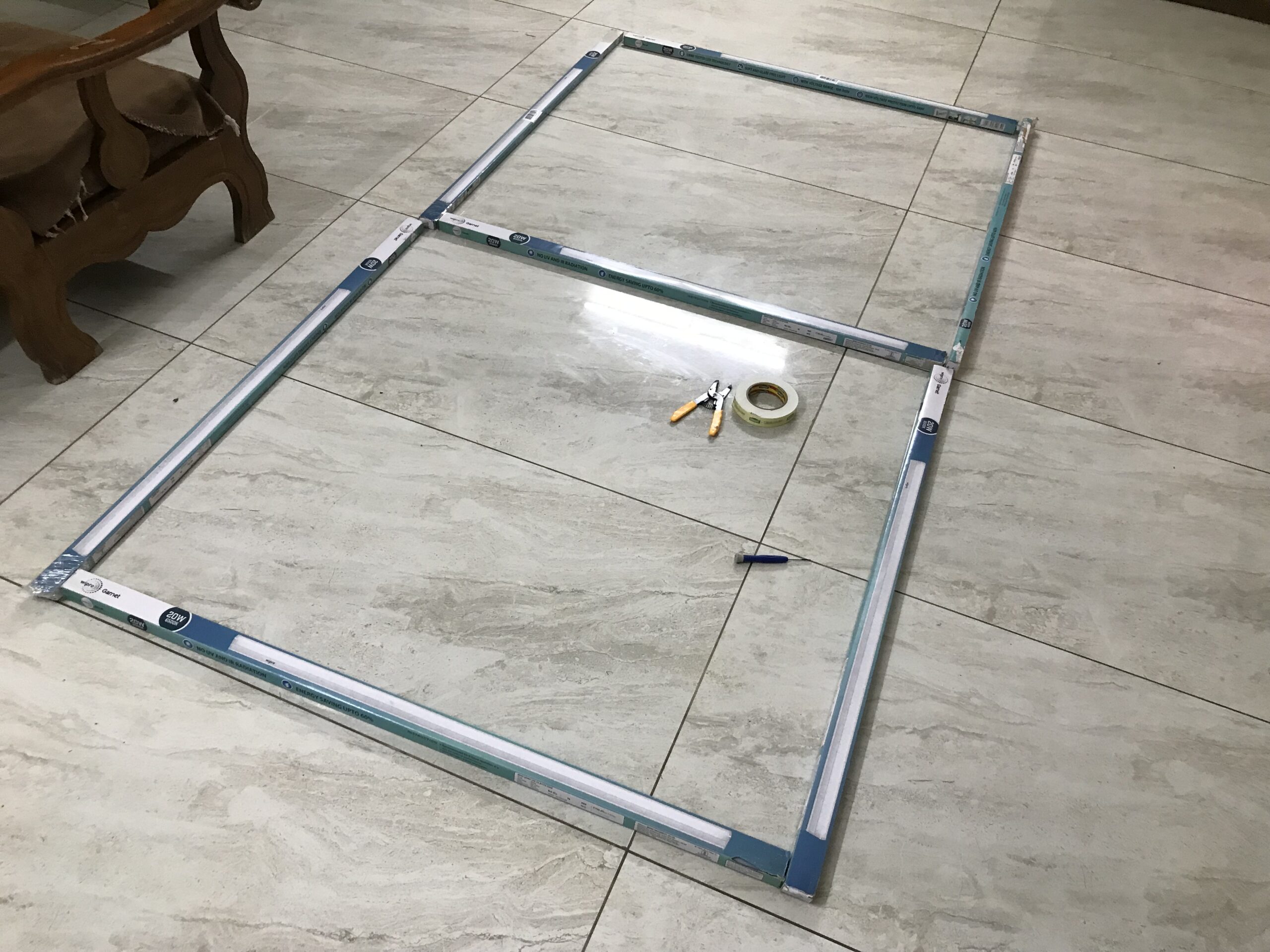
Controlling Large Size 7 Segment Display (Display size Approx. 8 Feet x 4 Feet)
We have created and tested a large-size 7-segment display with this board and an Arduino. Arduino example code is available as a download. Wiring between Arduino vs SPI 8 channel board as follows:
Pin 1:5V DC Output (200mA Maximum) >>Arduino 5V DC
Pin 2:SR/SRCLK/SH-CP (74HC595 Pin 11) >>Arduino Digital Pin D13
Each segment is made using 20W LED Batten (LED Tube Light) with Dimensions 113.5 x 2.8 x 6.8 cm, which works with 230V AC supply, user may use a smaller batten.
The project is tested with a single 7-segment display, but the user may use multiple displays with multiple boards, and use SPI outputs for other boards.
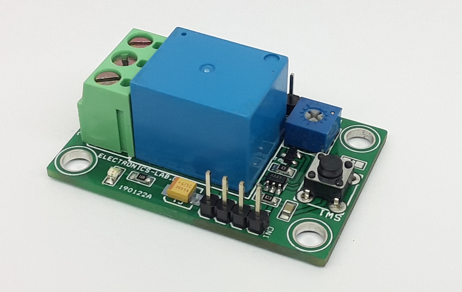
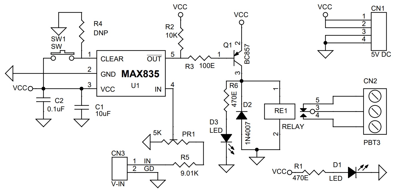
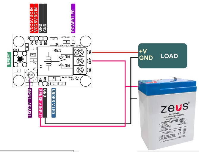
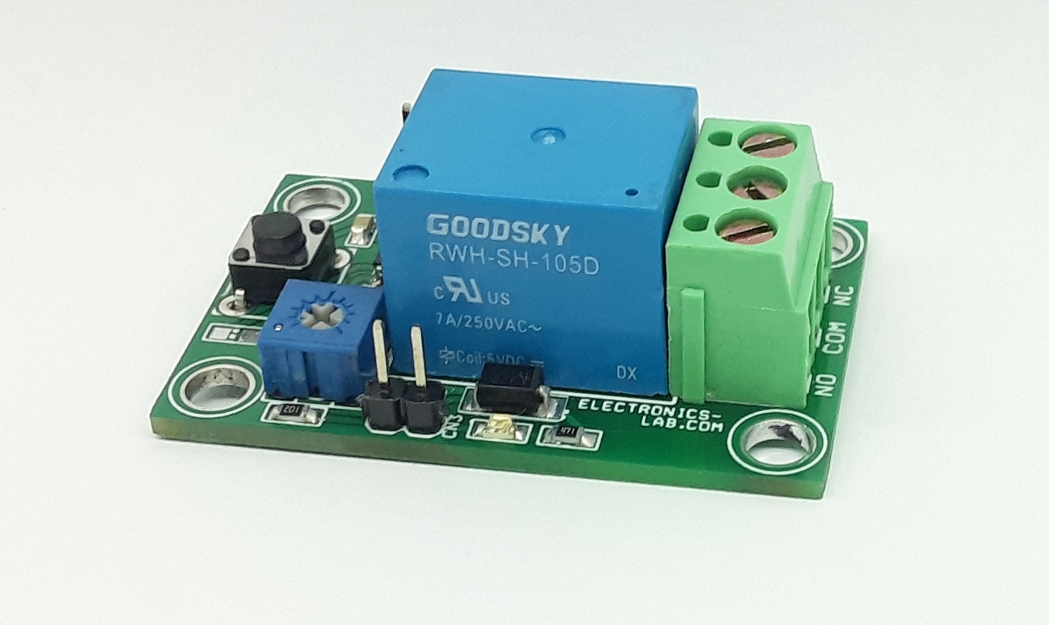
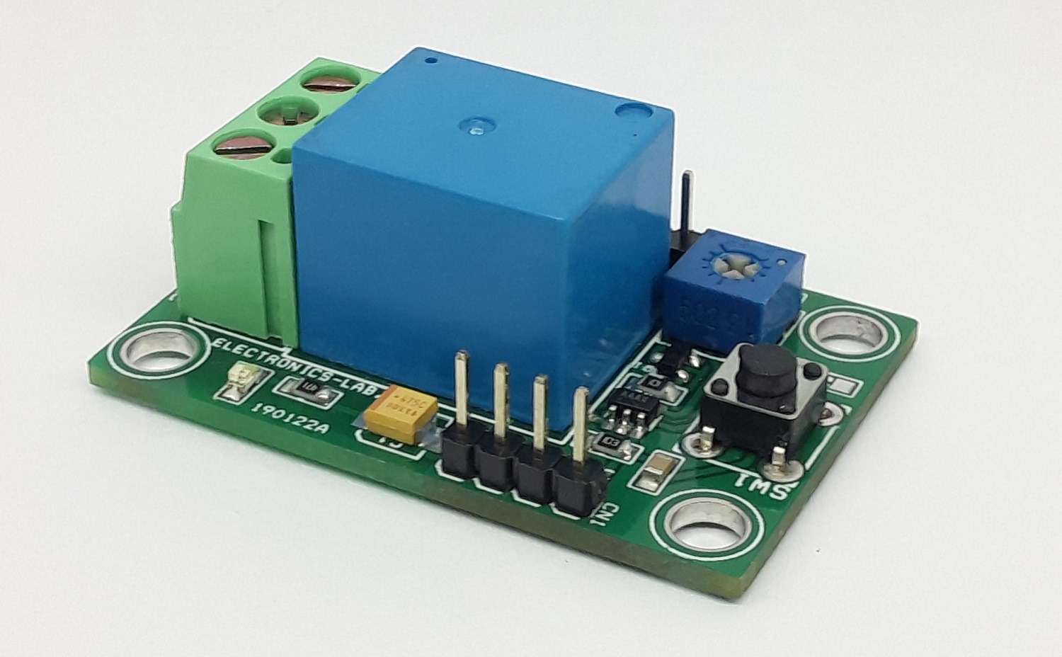
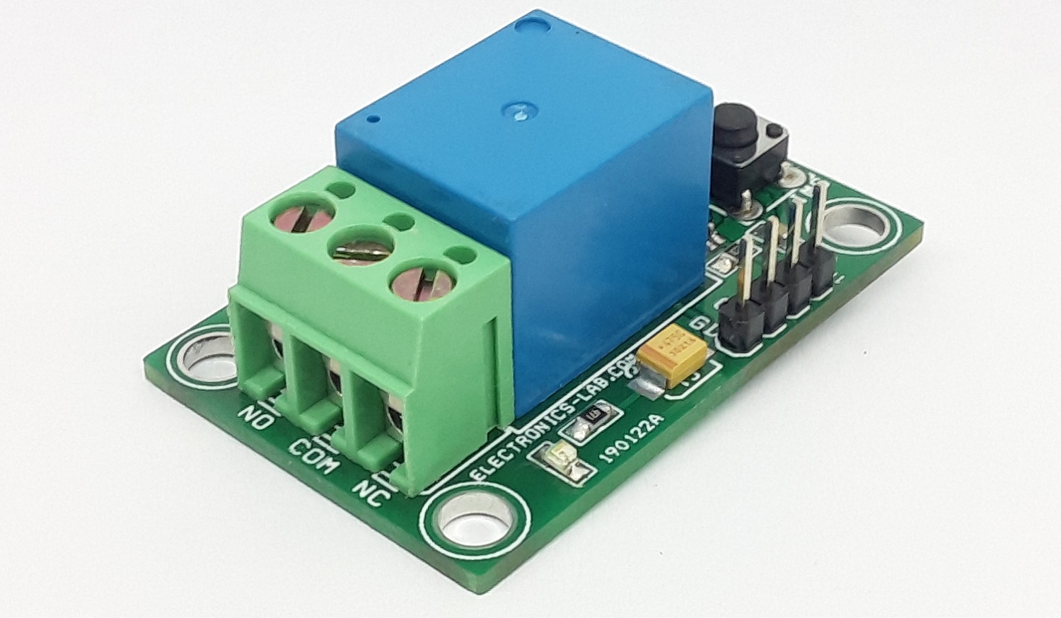
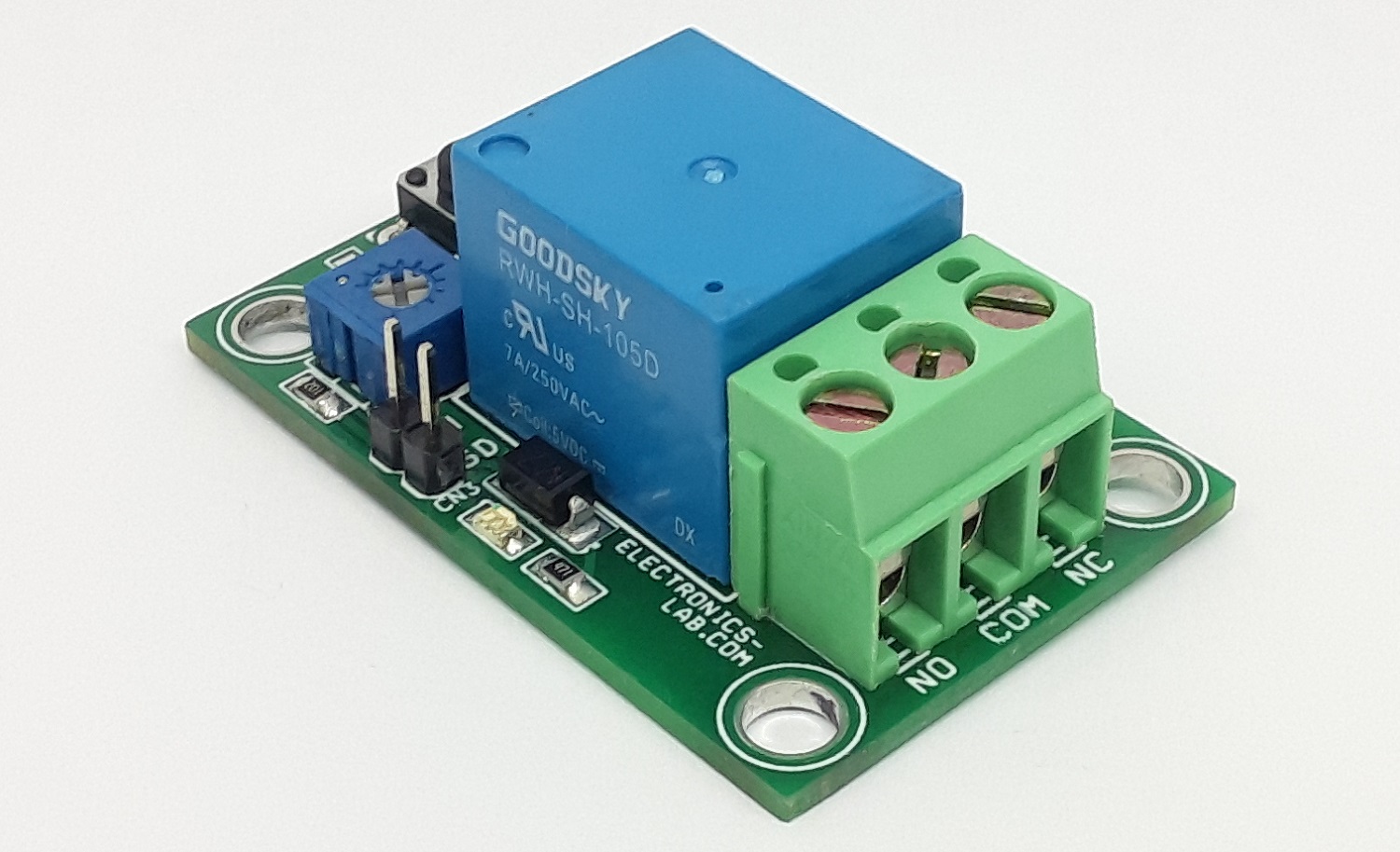
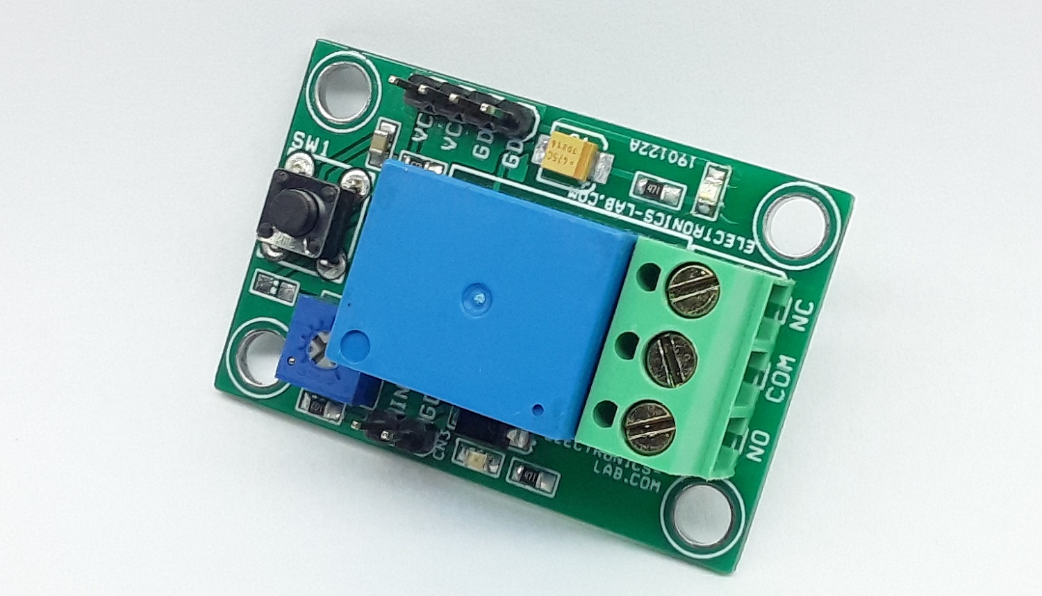
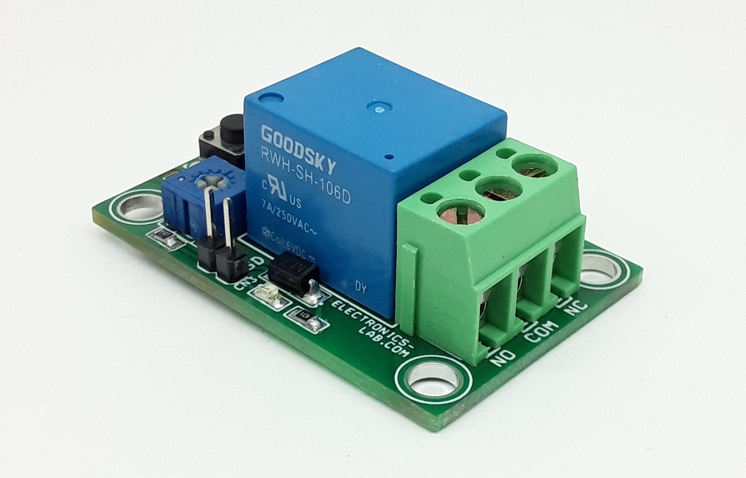
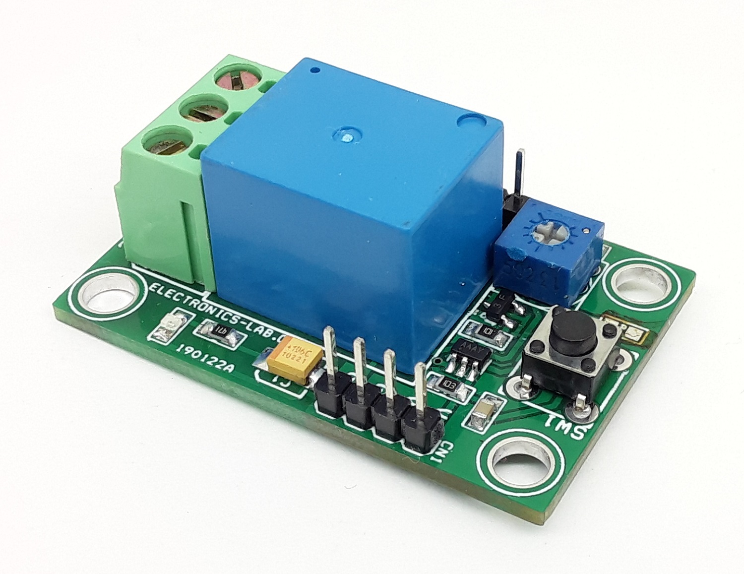
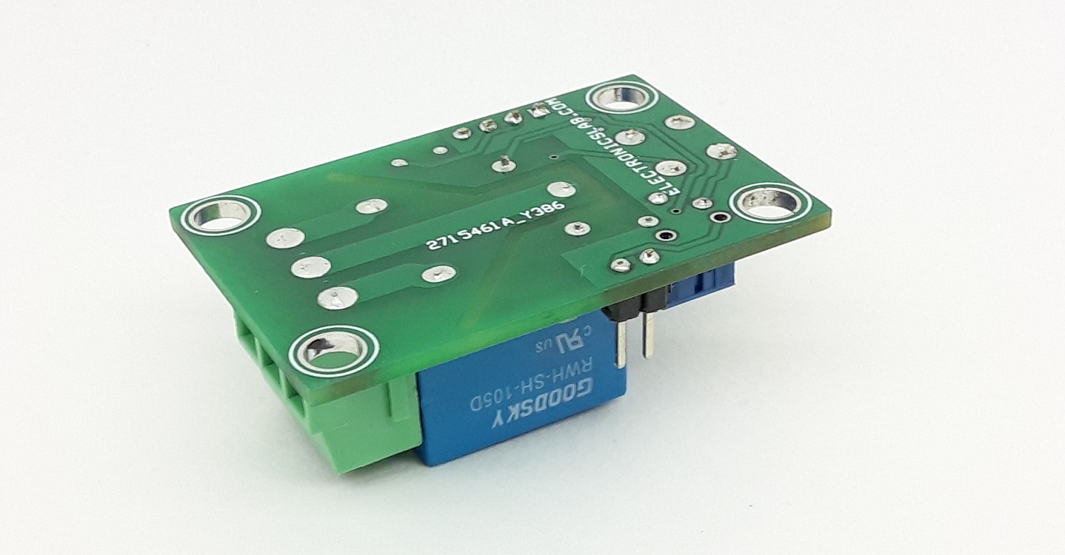
This project prevents/disconnects the load when an under-voltage condition occurs. The circuit latches the output when input sense voltage drops below the lockout threshold. Lockout threshold voltage can be adjusted using the onboard trimmer potentiometer PR1. Tactile switch SW1 is provided to reset the latch when input sense voltage is back to normal. The circuit consists of a MAX835 chip, 5V Relay, BC857 PNP transistor to drive the Relay, power LED, Relay/Output LED, and tactile switch. MAX835 chip features a level-sensitive latch, eliminating the need to add hysteresis to prevent oscillations in load-disconnect applications.
MAX835 micropower voltage monitors have a 1.204V precision bandgap reference, comparator, and latched output in a 5-pin SOT23 package. Using the latched output prevents deep discharge of batteries and disconnects the load from the power supply when Undervoltage is detected at input sense voltage. MAX835 has a push-pull output driver. Two external resistors set the trip-threshold voltage.
Operation
Connect an adjustable power supply to CN3 and apply input sense voltage in the range 3.4V to 8V, turn the PR1 trimmer potentiometer till the LED D3 is ON. Then the board is set for Undervoltage detection. For example, apply 4.90V to the CN3, rotate the PR1 so LED D3/Relay is on, the circuit is set for under-voltage detection threshold of 4.90V, now increase the input sense voltage to 5V and reset the latch using SW1.
Note 1: Relay contacts can handle load current up to 7A, use higher contact relay for high current load. Relays up to 16A are available with the same PCB footprint (same dimensions)
Note 2: The project can also be used to prevent deep discharge of batteries, it disconnects the load when battery voltage drops below the set point, read the datasheet of MAX835 to configure the input voltage range of battery using PR1 trimmer potentiometer and resistor R5.
Note 3: Input sense voltage range is 3.4V to 8V and can be adjusted using trimmer potentiometer PR1. The circuit can be configured to detect higher voltage. To achieve that choose the right value for PR1 and R5. Read the datasheet of MAX835 for more info.
Connections
CN1 = Pin1 VCC, Pin 2 VCC, Pin 3 GND, Pin 4 GND
CN2= Pin 1 Sense Voltage Input, Pin 2 GND
SW1 = Reset Switch
D1 = Power LED
D3 = Function LED – Relay Output
PR1 = Trimmer Potentiometer Input Sense Voltage Adjust
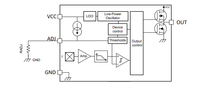
Texas Instruments TMAG5328Low-Power Hall-Effect Switch is a high precision, low-power, resistor adjustable Hall effect switch sensor with a low operating voltage. The TMAG5328 external resistor sets the operational BOP value. Users can follow a simple formula to calculate the resistor value needed to set up the correct BOP value. The Hysteresis value is fixed; therefore, the BRP value is defined as BOP Hysteresis.
The TI TMAG5328 Low-Power Hall-Effect Switch utilizes the adjustable threshold feature for easy and quick prototyping, fast design to market, reuse across different platforms, and easy last-minute modifications in case of unexpected changes. The device outputs a low voltage when the applied magnetic flux density exceeds the BOP threshold. The output stays low until the flux density decreases to less than BRP, and then the output drives a high voltage. By incorporating an internal oscillator, the device samples the magnetic field and updates the output at a rate of 20Hz for the lowest current consumption. The TMAG5328 supports an omnipolar magnetic response.
The TMAG5328 is housed in a standard SOT-23-6 package and operates from a VCC range of 1.65V to 5.5V.
Features
Supply range of 1.65V to 5.5V
Adjustable BOP from 2mT to 15mT
Using 2kΩ to 15kΩ resistors or 160mV to 1200mV voltage source
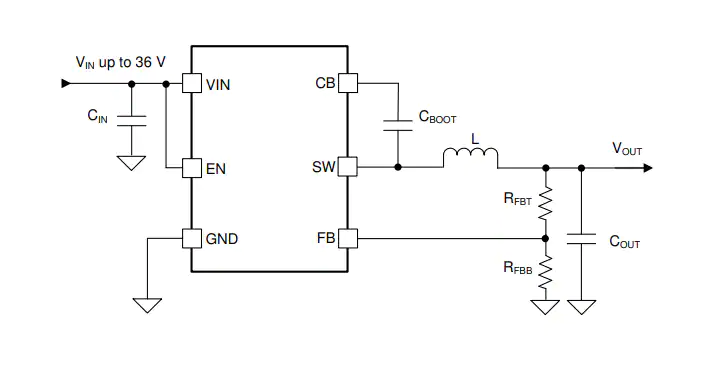
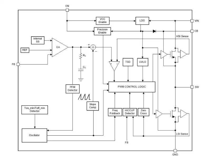
Texas Instruments LMR51430 SIMPLE SWITCHER® Buck Converters are easy-to-use with the capability of driving up to 3A load current. Offering a wide input range of 4.5V to 36V, the LMR51430 is ideal for a comprehensive range of industrial applications for power conditioning from an unregulated source. The 500kHz and 1.1MHz switching frequency on the device support the use of relatively small inductors resulting in an optimized solution size.
The TI LMR51430 Buck Converters provide a PFM version to achieve high efficiency at a light load and an FPWM version to attain constant frequency and small output voltage ripple over the entire load range. The device requires minimum external components with soft-start and compensation circuits implemented internally. Additionally, the LMR51430 offers built-in protection features, including cycle-by-cycle current limit, hiccup mode, short-circuit protection, and thermal shutdown in case of excessive power dissipation.
The LMR51430 is housed in a 6-pin SOT-23 package.
Features
Functional safety-capable
Documentation available to aid functional safety system design
Configured for rugged industrial applications
4.5V to 36V input voltage range
3A continuous output current
70ns minimum switching on time
500kHz and 1.1MHz fixed switching frequency options
–40°C to 150°C junction temperature range
98% maximum duty cycle
Start-up with pre-biased output
Internal short circuit protection with hiccup mode
±1.5% tolerance voltage reference
Precision enable
Small solution size and ease of use
Integrated synchronous rectification
Internal compensation for ease of use
SOT-23 package
Pin-to-pin compatible with the TPS54202 and TPS54302
PFM and forced PWM (FPWM) options are available
Create a custom design using the LMR51430 with the WEBENCH® Power Designer
SparkFun has just launched a new family of four boards: the Qwiic Micro, which offers popular breakouts in a really small footprint.
“Qwiic Micro is our smallest I2C-supported board form-factor yet!” says the company. “At only 0.75in. by 0.30in. (or 24.65mm by 7.62mm for metric friends), Qwiic Micro is perfect for projects and applications that have space or weight concerns.”
The new Qwiic micro family is smaller than the normal Qwiic board by more than a third, one may want to think that the company probably wants to get rid of their Standard Qwiic Board size of 1 x 1 inch but they have insisted that they have no plans for such as the new Qwiic Micro board family is just a new board size offering.
The new board family is said to be perfect for portable and other size-or-weight projects since they are way smaller than their full-scale predecessors. Though the boards did not come with the second Qwiic connector and the unpopulated 2.54mm pin headers as is in their full-size equivalents, they were duly compensated for by the presence of unpopulated ground and interrupt pins.
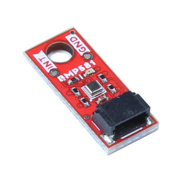
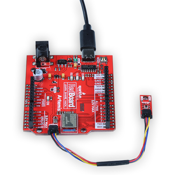
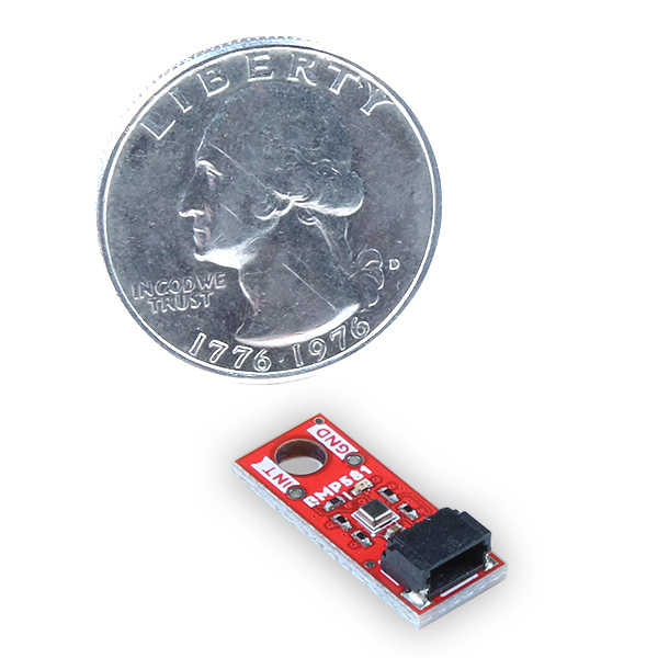
Qwiic Micro launches with four sensor boards: the first is with the BMP581 absolute Pressure Sensor from Bosch Sensortec, the second with the BMP384 pressure sensor from Bosch Sensortec also, the third with STMicroelectronics’ ISM330DHCX Six Degrees of Freedom IMU while the fourth with a triple-axis MMC5983MA magnetometer by MEMSIC. These breakouts are extremely small, you can install them in projects with exceptionally tight spaces. The Qwiic Micro Sensors communicate over I2C, so you don’t need any soldering to connect them to the rest of your project.
The Micro-sized SparkFun Qwiic BMP581 Absolute Pressure Sensor board – The BMP581 claims an exceptional resolution and accuracy of 1/64Pa. It uses on-chip linearization and temperature compensation to provide true absolute data for pressure and temperature. It also has a wide pressure sensing range of 30 to125 kPa as well as output data rates up to 622Hz. The minimum current consumption in all operating modes is just 1.5µA (typical) while the peak current consumption by the sensor is 260µA.
The SparkFun Qwiic BMP384 Pressure Sensor board – The BMP384 is a low-cost sensor with a high resolution of up to 21-bit. It consumes approximately 2µA when it is idle and ~700µA at peak during measurements. The sensor is not water-proof but it is a great option for monitoring pressure in humid environments as it provides extra resistance to liquid. The sensor also gives a very good accuracy in wide pressure and temperature ranges (300hPa to 1250hPa, -40 to +85°C).
The SparkFun Qwiic Micro ISM330DHCX Six Degrees of Freedom IMU – STMicroelectronics’ ISM330DHCX is a high-performance 3D digital accelerometer and 3D digital gyroscope tailored for smart applications. It has a full-scale acceleration range of ±2/±4/±8/±16 g and supports multiple modes that allow for peripheral only, secondary I2C, and auxiliary three or four-wire serial interface. It also has a wide angular rate range of ±125/±250/±500/±1000/±2000/±4000 dps that enables its usage in a broad range of applications as well as an unmatched set of embedded features (Machine Learning Core, programmable FSM, FIFO, sensor hub, event decoding and interrupts).
The board is perfect for applications such as optical image, lens stabilization, robotics, and industrial automation, navigation systems, and vibration monitoring and compensation.
The SparkFun Qwiic Micro MMC5983MA Magnetometer – The highly sensitive MMC5983MA Magnetometer can sense down to 0.4 mG, with a heading accuracy of ±0.5°. It is said to be ideal for electronic compass applications; has output rates of 1000Hz, ±8G FSR, and 18-bit resolution.
All four boards are very much available and sell for affordable prices. The BMP581 goes for $20.95, the BMP384 for $16.95, the ISM330DHCX for $25.95, and the MMC5983MA for $15.95.
Edge Impulse has announced support for Arduino’s compact Nicla Sense ME board targeted at Edge AI Motion and Environment projects — a new standard for intelligent sensing solutions. The edge AI and tinyML expert promised to give full support for the device’s newly integrated sensors.
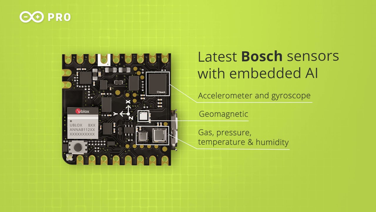
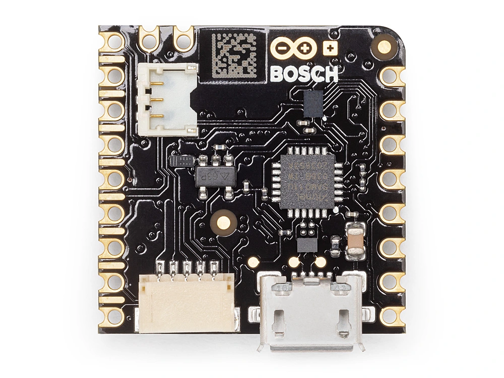
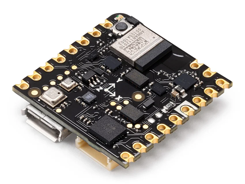
Less than a year ago, in September 2021, Arduino partnered with Bosch’s sensor division to launch the Nicla Sense ME, development board, with a stamp-like ultra-compact design. The high-performance, low-power board was designed to bring smart sensing solutions to the edge.
“Its small size and robust design make it suitable for projects that need to combine sensor fusion and AI capabilities on edge, thanks to a strong computational power and low-consumption combination that can even lead to stand-alone applications when battery operated,”
Edge Impulse’s Jenny Plunkett explains the compact development board.
Features and Specifications Include:
64 MHz Arm® Cortex M4 (nRF52832) microcontroller
Bluetooth® 4.2 connectivity
512KB Flash / 64KB RAM, 2MB SPI Flash for storage, 2MB QSPI dedicated for BHI260AP
1x I2C bus (with ext. ESLOV connector), 1x serial port, 1x SPI, 2x ADC, programmable I/O voltage from 1.8-3.3V
Power: Micro USB (USB-B), Pin Header, 3.7V Li-po battery with Integrated battery charger
Dimensions: 22.86 mm x 22.86 mm
Weight: 2 grams
Usage and Applications:
Predictive maintenance
Robotics
Accelerated medical recovery
Logistics and supply chain
Gas detection
Detection of toxic substances
Home Automation
Monitoring of environmental conditions
Edge Impulse also extended support to four state-of-the-art sensors from Bosch Sensortec:
BHI260AP motion sensor system with integrated AI
BMM150 magnetometer
BMP390 pressure sensor, and,
BME688 four-in-one gas and environment sensor with AI and integrated high-linearity.
With the range of Bosch Sensortec hardware and the powerful Nordic SeminRF52832 system-on-chip, the Nicla Sense ME compact development board can be used to easily measure and analyze rotation, acceleration, temperature, pressure, humidity, air quality and CO2 levels.
Here are some of the benefits you get with using the Arduino Nicla Sense ME Development Board:
It has tiny size, yet is packed with amazing features
It has a low power consumption rate
It adds sensing capabilities to existing projects
It becomes a complete standalone board when battery-powered
It has a very powerful processor, capable of hosting intelligence on the Edge
Robust hardware including high-quality Bosch sensors with embedded AI (accelerometer, gyroscope, geomagnetic, gas, pressure, temperature & humidity sensors)
Bluetooth LE connectivity maximizes compatibility with professional and consumer equipment
It can measure motion and environmental parameters easily (motion, gas, pressure, temperature, humidity, and more)
Always-on sensor data processing at extremely low power consumption
It is compatible with Arduino Portenta and MKR families
Battery or USB powered
Video
The company provided a quick guide on how to get started with the board; flashing the Nicla Sense ME with the Edge Impulse firmware for data collection and inference.
“Once you have collected enough data samples from your desired sensor, you can follow the building of a continuous motion recognition system tutorial to develop and deploy a machine learning model using one of the many Bosch sensors on the Nicla Sense ME,” says Plunkett.
These details and other useful information on the Nicla Sense ME development board can be found on the documentation site or on the Arduino Store where it sells for $82.80.
The numbers used in real life for routine financial matters, numeric records, and in mathematical calculations, etc. are either positive or negative in sign. The positive numbers are usually unsigned and do not carry a positive (+) sign. Moreover, a number without any sign is understood to be a positive number. Contrary to this, a negative number is a signed number that is represented by a negative sign (-) on the leftmost side of the number e.g. -12345 or -1234510.
The binary numbers, which are discussed in the previous articles, are unsigned binary numbers i.e. positive values only. As the architecture of digital systems and computers understand only binary numbers, the representation of real-life signed numbers in binary by a positive (+) or negative (-) sign is not possible. Because the binary numbers are represented by binary digits (bits) which can have a value of either “0” or “1” i.e. they can have only two numbers to represent a bit. The bit value either “0” or “1” is a mere representation of the logic level which is dependent on the digital circuit. That said, representation and understanding of any other number besides “0” and “1” are not possible at the hardware level of the digital system. Contrary to decimal numbers, it is not possible to include a negative sign with a binary number to represent a negative value.
Sign-and-Magnitude
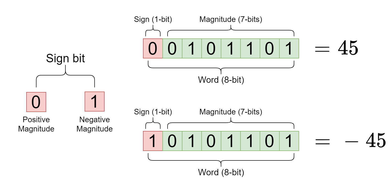
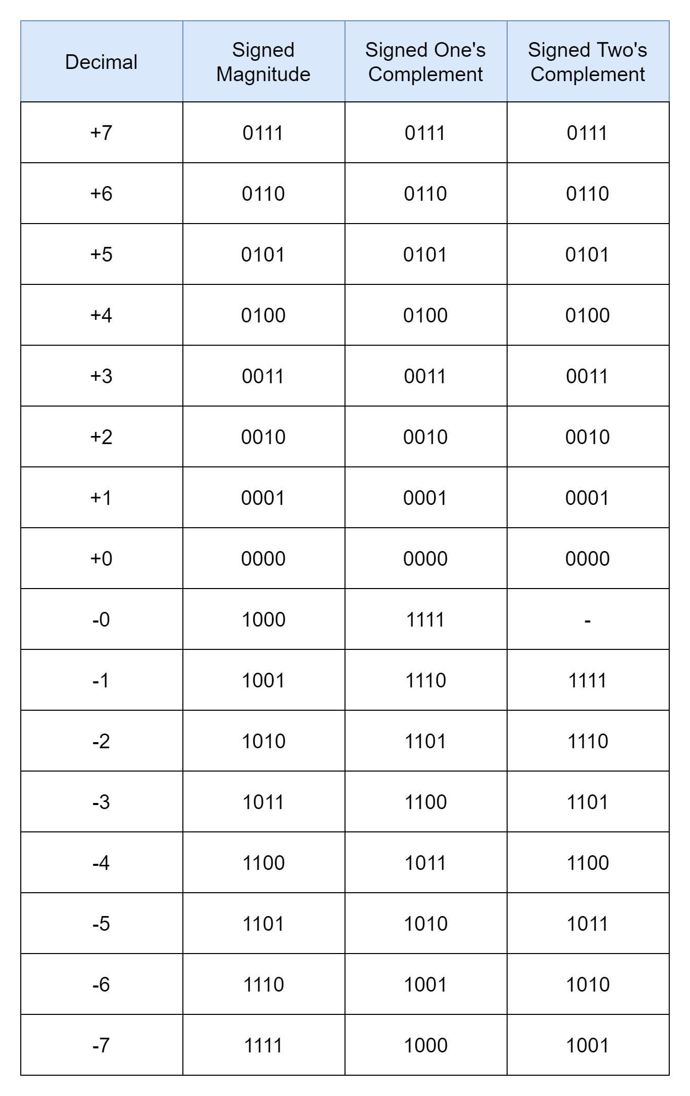
A number, essentially, should have two values i.e. sign and magnitude in order to represent positive and negative values. This representation is known as Sign-and-Magnitude (SM) notation. For example, a negative number (-12345) is represented by using this Sign-and-Magnitude (SM) notation. This method, Sign-and-Magnitude, is the simplest and most commonly used method to represent numbers both positive and negative. The Sign-and-Magnitude method can also be applied to binary numbers to represent negative and positive numbers. The binary number carrying a sign (positive or negative value) along with the magnitude is termed signed binary numbers.
The binary number is represented by only “0”s & “1”s and there is no provision to include (+) or (-) sign in order to use Sign-and-Magnitude notation. In order to adopt this Sign-and-Magnitude method, the most significant bit (MSB) is used as a sign to indicate the positive or negative value of the binary number. For representing, a positive signed binary number a “0” is used as a most significant bit, whereas, a “1” represents a negative signed binary number. Using this Sign-and-Magnitude notation, the most significant bit of a signed binary number holds the sign (positive or negative notation) and the rest of the bits represent the magnitude or value of the signed binary number.
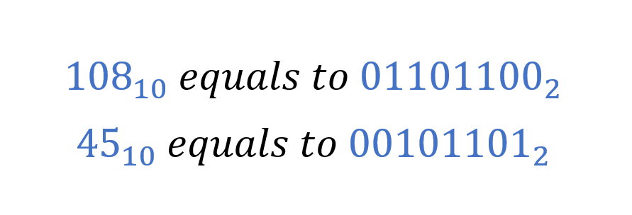
The signed binary number having “n” number of bits uses one (1) bit to indicate the sign and “n-1” bits to represent the magnitude or value. Using the Sign-and-Magnitude notation, the positive and negative value of a decimal number (45) is represented below as a signed binary number. The decimal number can be converted to a binary value by using the repeated-division-by-2 method which is discussed in the previous article.
Figure 1: The Sign-and-Magnitude notation of Signed Binary Numbers
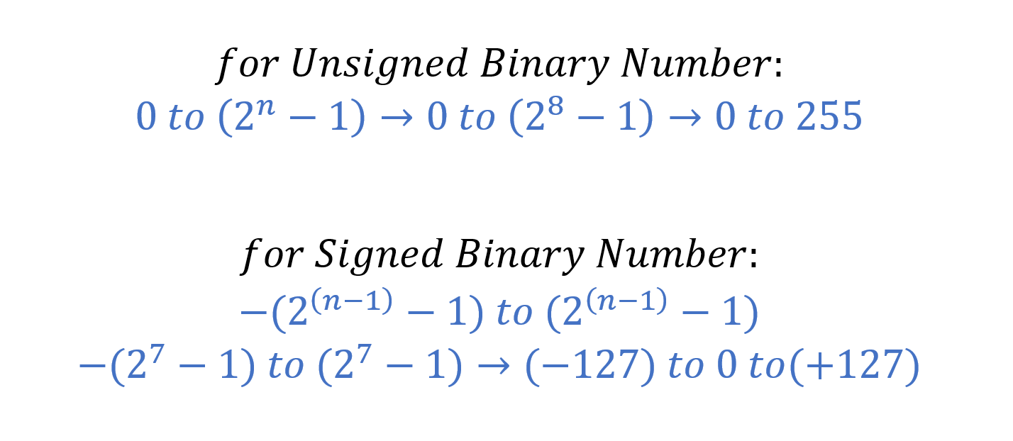
However, the Sign-and-Magnitude notation has a number of disadvantages. The usage of one (1) bit as a sign bit reduces the number of bits to hold the magnitude or value. In a comparison with an unsigned binary number having “n” number of bits, the signed binary number is going to have “n-1” bits to represent a value. The sign-and-magnitude notation splits the number values into two halves i.e. one on each side of zero (0). In order to understand this, the decimal ranges of unsigned and signed binary numbers are given below. The size of both unsigned and signed numbers is set to eight (8) bits.
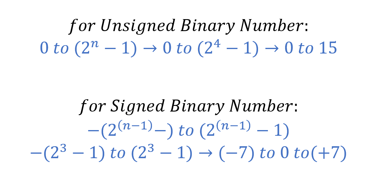
The range of numbers for an eight (8) bit unsigned number is from “0” to “255” i.e. a total of 256 numbers that can be represented. Whereas, the signed binary number ranges from “–127” to “127” including the middle value of “0”. The number of values represented by the signed number is “255”. Likewise, for the 4-bit unsigned and signed binary numbers the decimal ranges are:
Similarly, the ranges for 4-bit unsigned and signed binary numbers are (0 to 15 = 16) and (-7 to +7 = 15), respectively. Here, again, the sign-and-magnitude notation has reduced the number of values by one (1) compared to the equivalent unsigned binary number.
Besides, the sign-and-magnitude notation has two zero (0) values each representing a positive and negative zero. For example, a sign bit of “0” placed with a “0” value shows a positive zero i.e. 00002. Likewise, a sign bit of “1” placed with “0” values shows a negative zero i.e. 10002. According to sign-and-magnitude notation, both are valid and this occupies one of the number values discussed above.
Signed Binary Number Examples
In the following table, a number of examples are given to represent both positive and negative decimal numbers with their equivalent signed binary numbers. The conversion from decimal to binary number is achieved by the application of the repeated-division-by-2 method.
In order to use sign-and-magnitude notation, the sign bit is placed at the most significant bit (MSB), whereas, the rest of the bits represent magnitude or value. If the magnitude or value is less and does not occupy all of the magnitude bits then the remaining magnitude bits are set to zero (0). This arrangement helps in identifying the sign bit’s location i.e. MSB of 8-bit, 16-bit, or 32-bit, etc.
One’s Complement
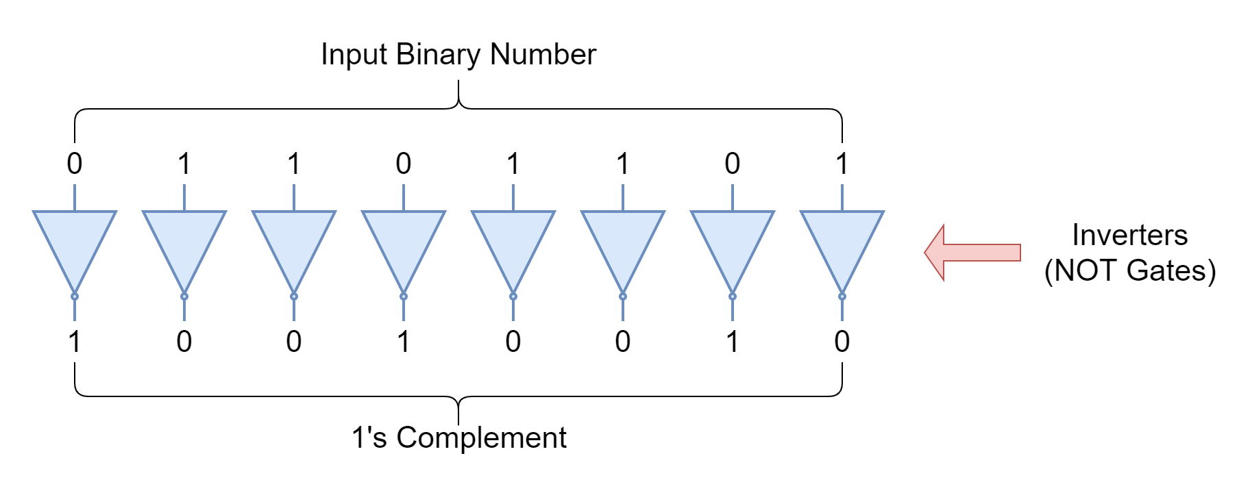
The One’s Complement is another method to represent negative numbers of a signed binary number. The positive values remain unchanged and are, as such, called non-complemented values. The positive values are the same as shown for sign-and-magnitude positive values. However, the negative values are one’s complement that is inverted or negated. For example, the complement of “0” is “1” and of “1” is “0”. Therefore, the negative of a given positive signed binary number can be determined by taking one’s complement or changing “0”s to “1”s and vice versa. For example, the one’s complement of 101100112 is 010011002. In digital or logic circuits, one’s complement is achieved by using “Inverters“. The number of parallel inverters required is dependent on the size or length of the signed binary number (number of bits).
Figure 3: Implementation of 1’s complement using NOT Gates
Similar to the sign-and-magnitude notation, the one’s complement has n-bit notation ranging from –(2n-1-1) to (2n-1-1) and has two values to represent a zero i.e. 00002 (positive) and 11112 (negative) for a 4-bit signed number.
Addition and Subtraction using One’s Complement
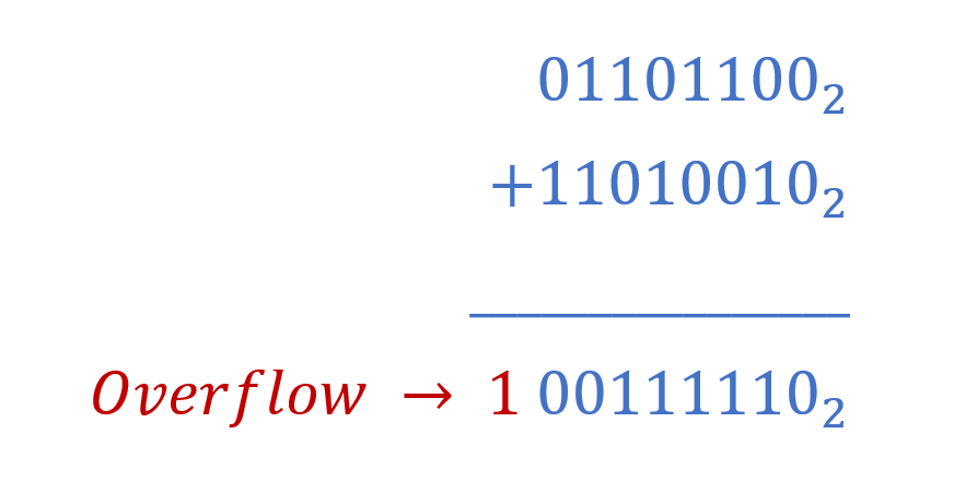
The one’s complement can be used to subtract binary numbers. The addition of two binary numbers is achieved by using Adder circuits resulting in Sum and Carry bits. The Adder result depends on the values of the input values. In mathematics, the subtraction of numbers can be formulated as A + (-B) which is the addition of two numbers having inverted to be subtracted operand. Using this formulation, the subtraction of two binary numbers can be performed by using one’s complement on the desired operand. For example, the mathematical expression 108 – 45 = 63 is performed carried out using one’s complement.
The decimal numbers are converted into equivalent decimal numbers and both binary numbers are adjusted to 8-bits by adding leading zeroes.
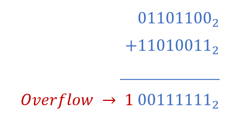
In order to subtract 4510 from 10810 using addition or adder, the one’s complement of 4510 is determined by inverting its every bit. The equivalent binary of 4510 is 001011012 and its one’s complement is 110100102. Now, this one’s complemented added to 10810 = 011011002 gives the one’s complemented subtraction as shown below.
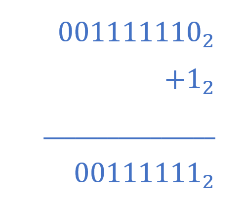
In the above result, the 9th bit is an overflow bit and indicates subtraction resulted in a positive number. If subtraction results in no overflow bit then the result is a negative number. So, in this case of overflow, the 9th bit or overflow bit can be safely ignored. Now, to convert this one’s complemented result into a real result, a “1” is added as shown below.
The subtraction using one’s complemented produced the result (001111112) which when converted to the equivalent decimal number is 6310. The equivalent decimal number of (001111112) is determined using the sum of the weighted product i.e. (32+16+8+4+2+1) = 63. So, one’s complement can be used in binary adders such as 74LS83 or 74LS283, etc. to subtract the signed binary numbers.
Two’s Complement
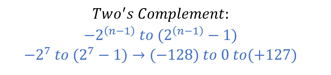
The two’s complement is another method to represent the negative binary number in a signed binary number system. Just like Sign-and-Magnitude and One’s Complement methods, the positive binary numbers remain unchanged. Whereas, a negative number in two’s complement method is one’s complemented plus (+) “1” to the least significant bit (LSB). The negative binary number when added to its counterpart positive number results in zero. The two’s complement does not include the double zeros issue which was observed in Sign-and-Magnitude and One’s Complement methods. Further, it is much easier to obtain two’s complement making arithmetic operations relatively much easier. The range of two’s complement signed binary number is given below.
Using the previous example of one’s complement, the two’s complement of (4510 = 001011012) is obtained by first getting one’s complement and adding “1” to it i.e. (110100102 + 000000012 = 110100112).
The two’s complement of 4510 equals -4510 in a signed binary number. The subtraction (10810 – 4510) is, thus, obtained by adding both signed binary numbers as shown below.
The overflow bit is discarded and the rest of the 8-bits constitute the subtraction result which is equivalent to (6310 = 32+16+8+4+2+1).
In the following table, a comparison of different methods to represent 4-bit signed binary numbers is shown.
Conclusion
The signed binary number system is used to represent both positive and negative numbers in binary. The methods used to represent signed binary numbers are Sign-and-Magnitude, One’s Complement, and Two’s Complement.
The Sign-and-Magnitude uses the most significant bit (MSB) as a sign bit. The zero (0) shows a positive magnitude and a one (1) shows a negative magnitude of a binary number. The range of numbers is split into -127 to -0 and +0 to +127. The disadvantage involves double zeros i.e. 00002 and 10002.
In One’s Complement method, the positive numbers remain unchanged whilst the negative numbers are obtained by inverting each bit of its relevant counterpart positive. The range of numbers is split into -127 to -0 and +0 to +127. Similar to Sign-and-Magnitude, the One’s Complement has the disadvantage of having double zero in its range of numbers. The addition or adder can be used along with one’s complement to perform the subtraction of two binary numbers.
The Two’s Complement has unaltered positive numbers just like Sign-and-Magnitude and One’s Complement methods. The negative number is obtained by first determining the one’s complement of the relevant positive number and then adding “1” to it. The range of numbers is -128 to 0 to +127 and includes only one zero in the range.
The two’s complement is the most commonly used method to represent signed binary numbers compared to other presented methods. The usage of the two’s complement method avoids the issue of double zero and the arithmetic operations become relatively much easier.
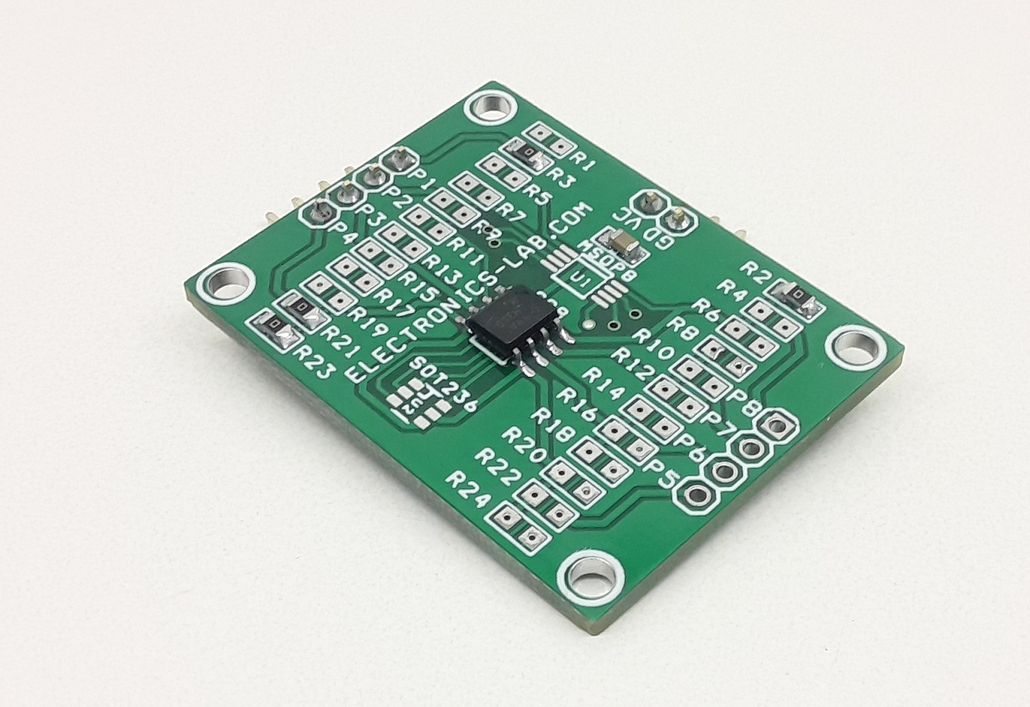
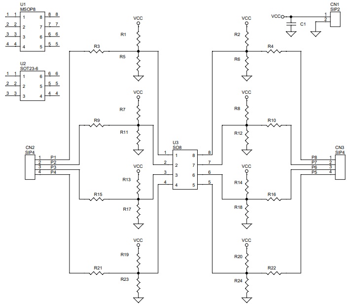
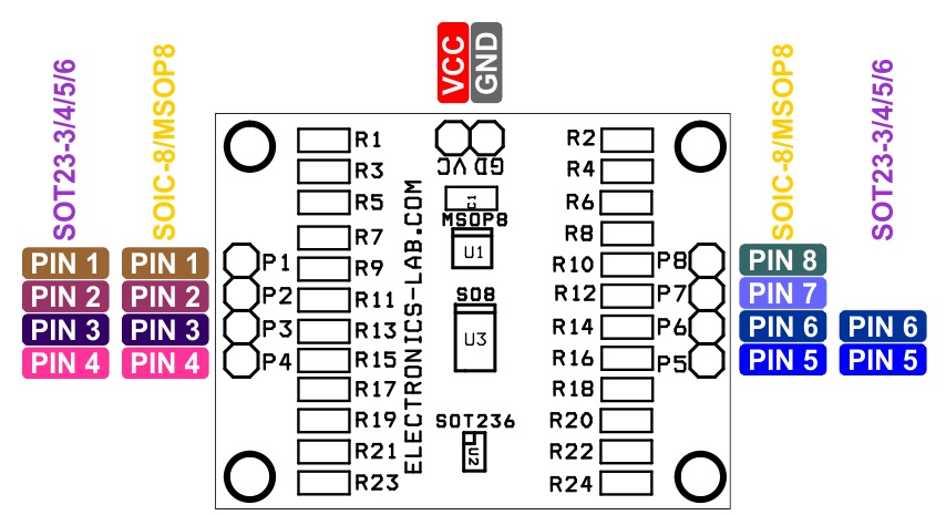
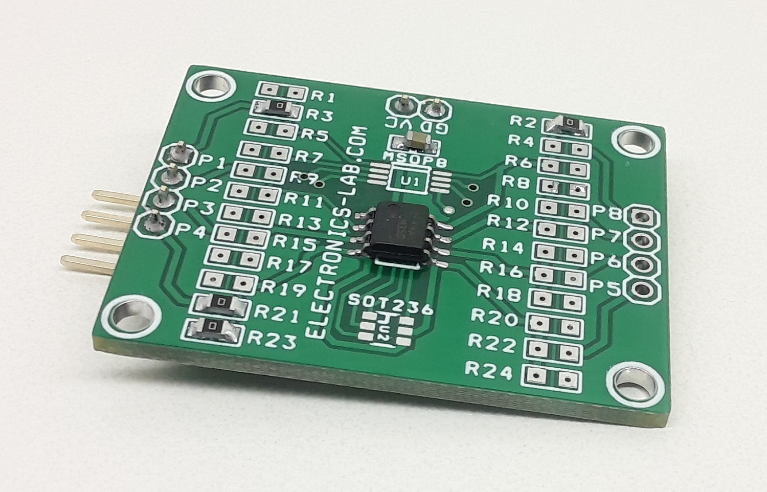
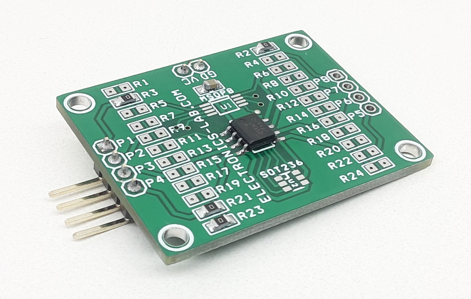
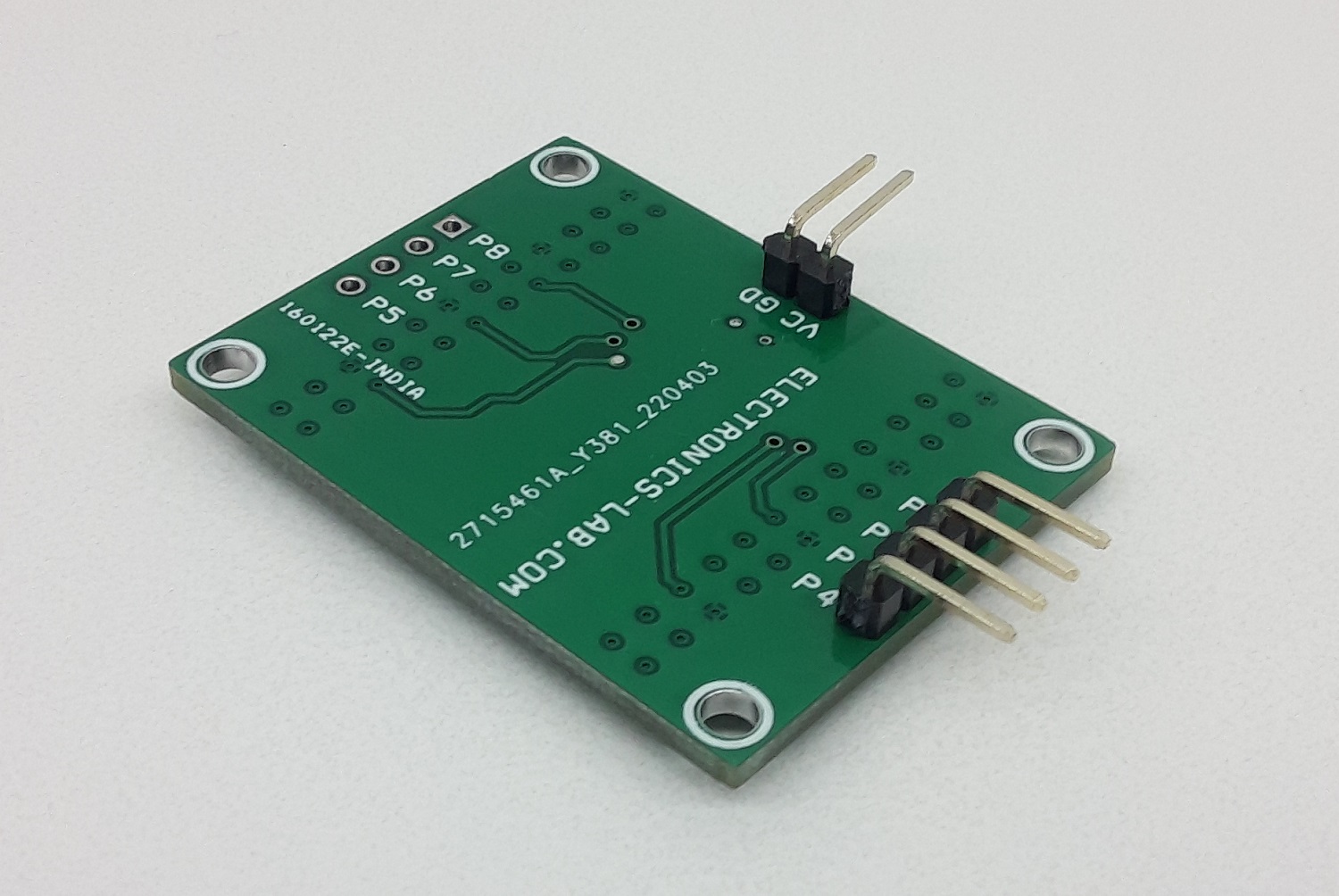
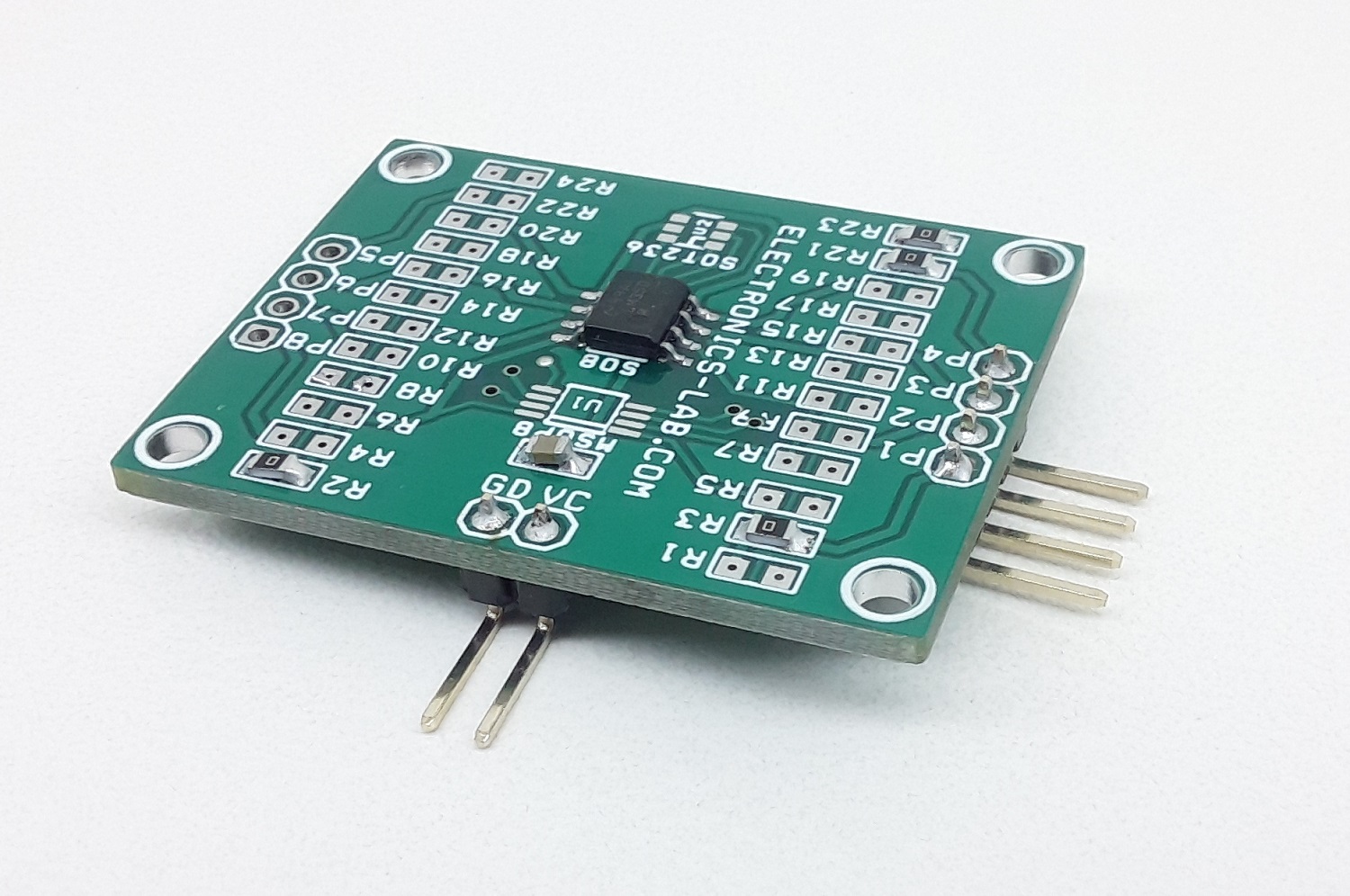
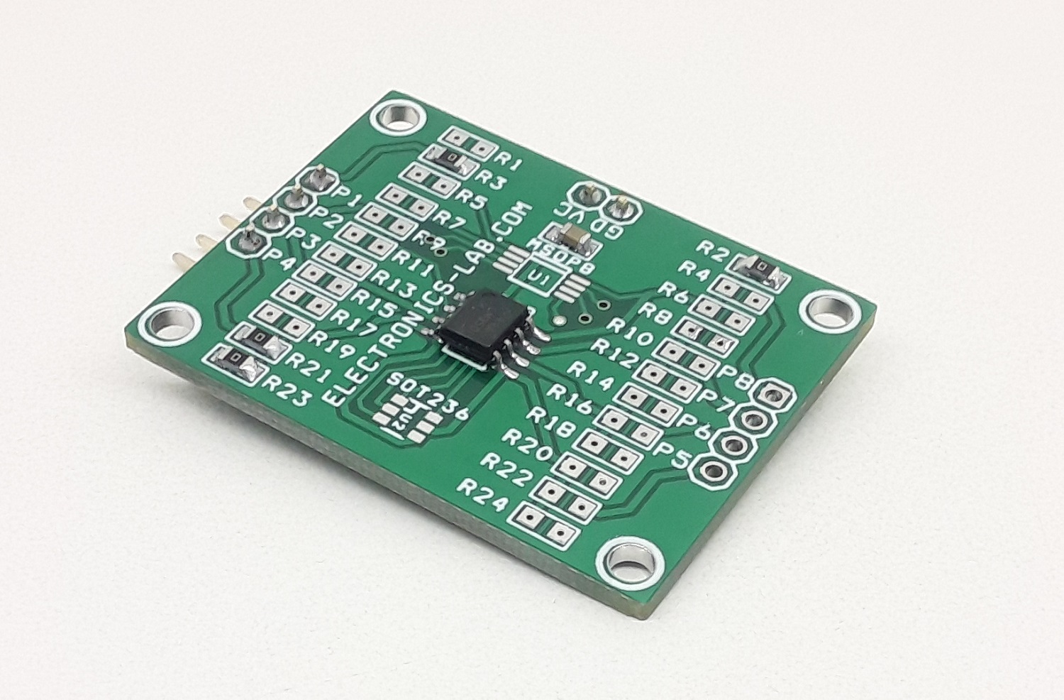
This is an 8-pin SOIC/MSOP/SOT23-3/4/5/6 prototype board. This is a blank PCB that allows the operation of many chips from various manufacturers. Each device pin is connected to a pull-up resistor, a pull-down resistor, an in-line resistor, and a capacitor on VCC. All pins are provided with a male header connector.
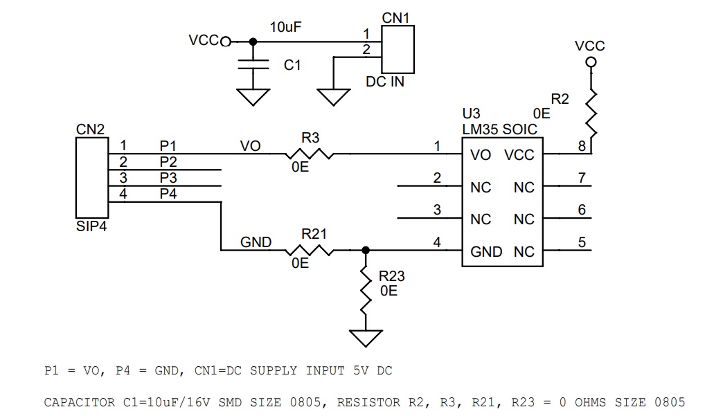
Note: Example schematic of temperature sensor LM35 provided.
Features
Supports 8-pin SOIC package
Supports 6-pin SOT23-3/4/5/6 (TSSOP) package
Supports 8-pin MSOP package
All Resistors and capacitor Size 0805
Each device pin has a footprint for an optional pull-up resistor, a pull-down resistor, In line resistor
2 Pin Male Header connector and power supply filtering capacitors