A rechargeable battery’s load should be disconnected at the point of complete discharge, to avoid a further (deep) discharge that can shorten its life or destroy it. Because a battery’s terminal voltage recovers when you disconnect the load, you can’t simply disconnect the load when the terminal voltage dips below the established threshold and then re-connect it when the voltage returns above that threshold. Such action may produce chatter in the disconnect switch. The project shown here is a complete solution to this problem.
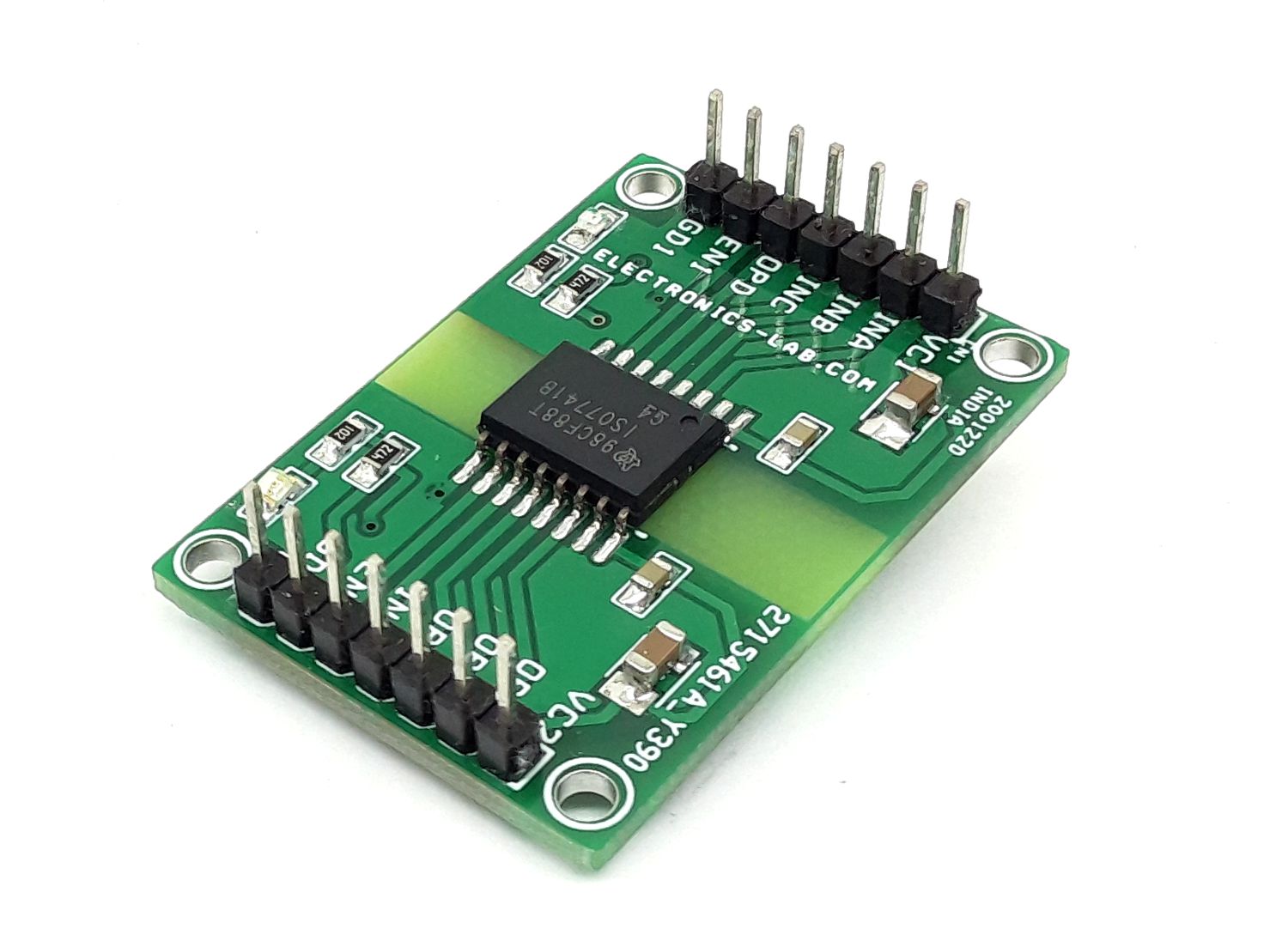
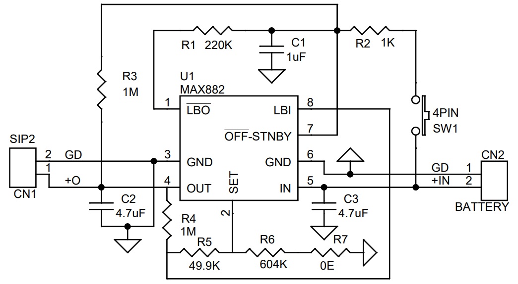
The circuit disconnects the load when the battery level goes below a set point. The project is built using the MAX882 chip, which has a low-battery comparator and error amplifier that share the internal reference and the external resistor divider. With the resistor values shown, the low-battery output (LBO) goes low and disconnects both the battery and load when the output falls eighty percent below its nominal value. The battery and load then remain disconnected until RESET is clicked by SW1. Two factors enable the latching action in this circuit: the low-battery comparator remains active during shutdown (most regulators deactivate this comparator during shutdown), and the circuit monitors the regulated output voltage instead of the battery voltage (regulator voltage can’t recover until the regulator is turned back on). The circuit also provides an active-low POWER FAIL signal (LBO, pin 1) that goes low 50ms before the output is turned off. When LBO goes low, C1 discharges through R1 until the active low STBY input reaches its threshold (1.15V). The IC then enters its standby mode and disconnects the battery. IC1 is a linear regulator capable of sourcing 150mA with a 350mV dropout voltage. It has a 10µA standby current.
The disconnect voltage level is set to 3.08V. When the battery voltage drops to 3.08V, it disconnects the load, to reverse the condition, recharge the battery or replace and press the SW1.
Circuit Credits: Maxim Semiconductor
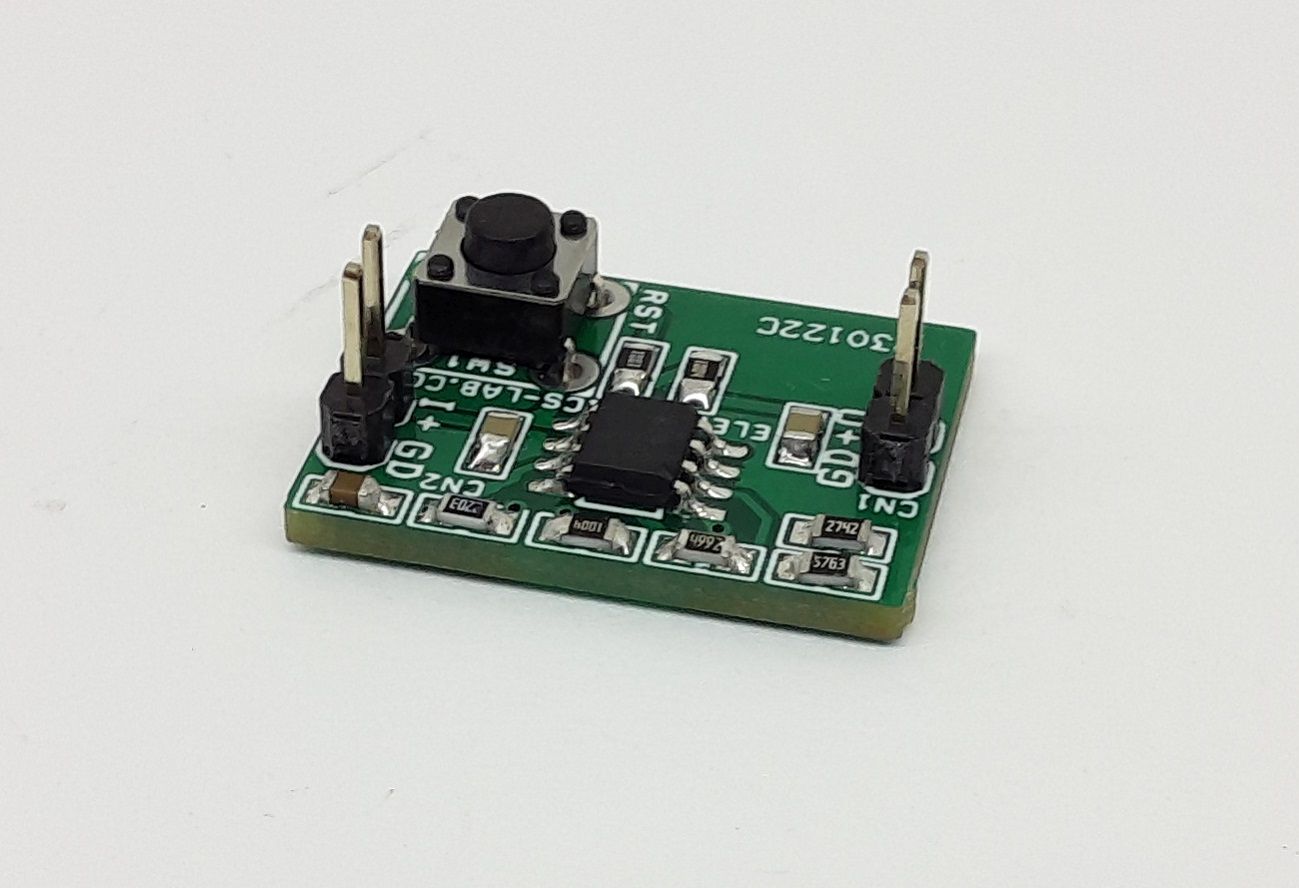
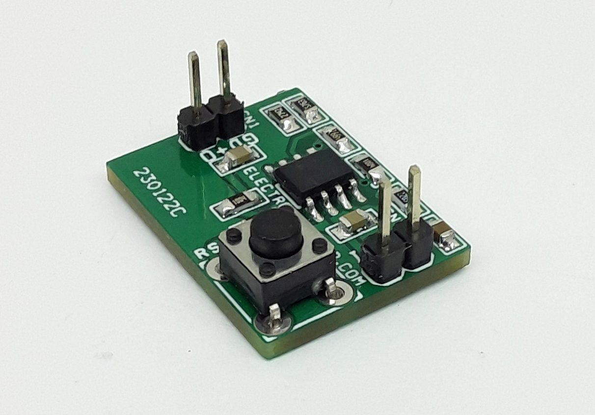
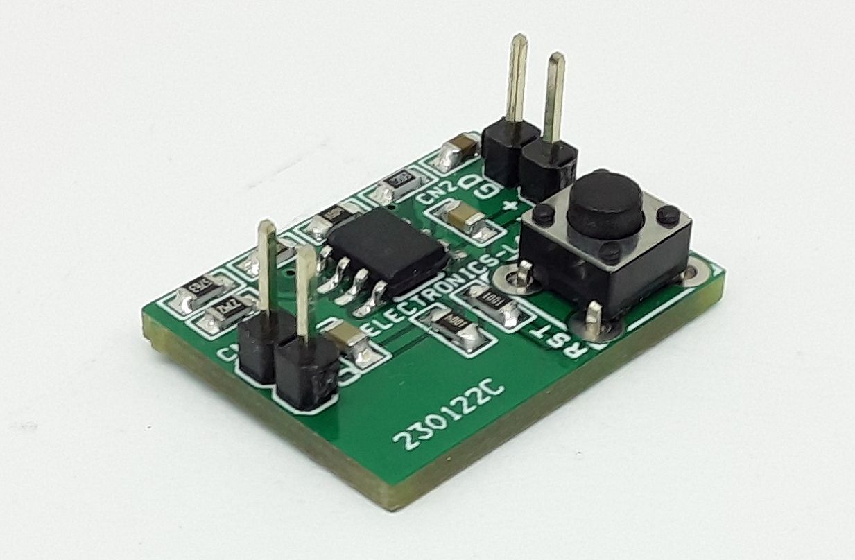
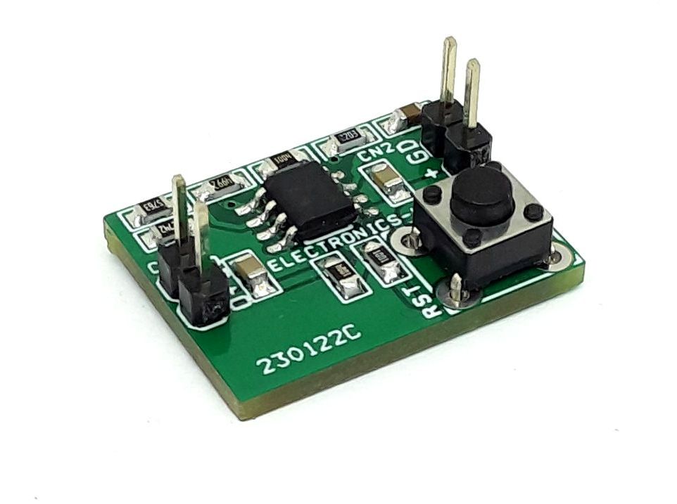
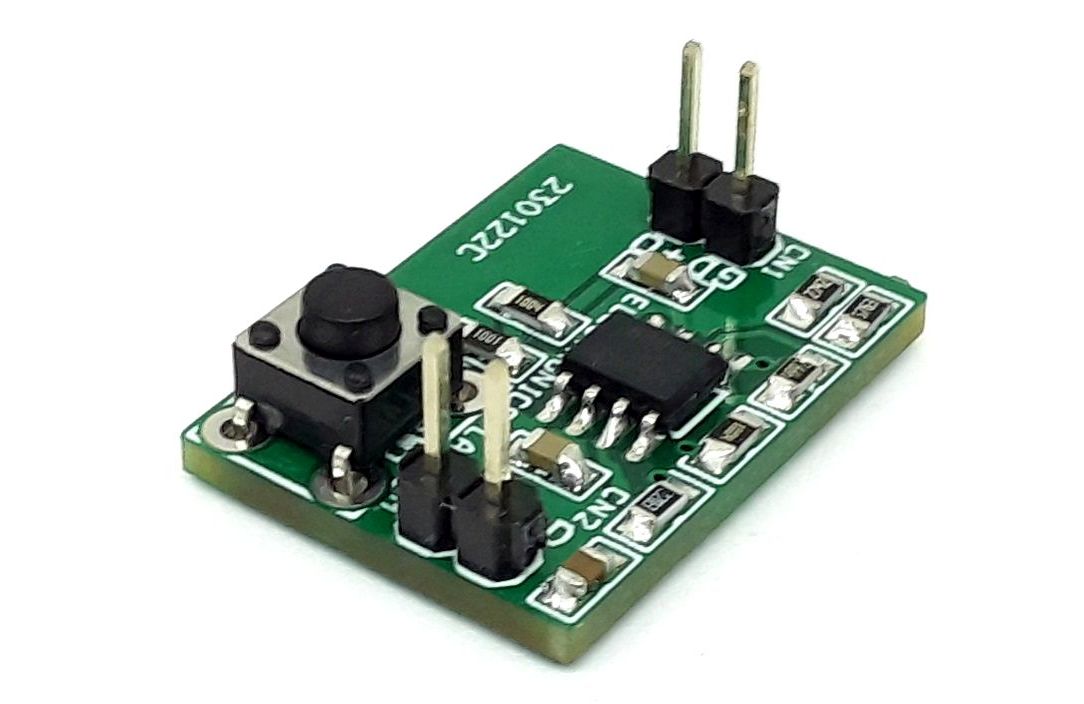
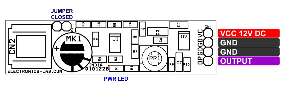
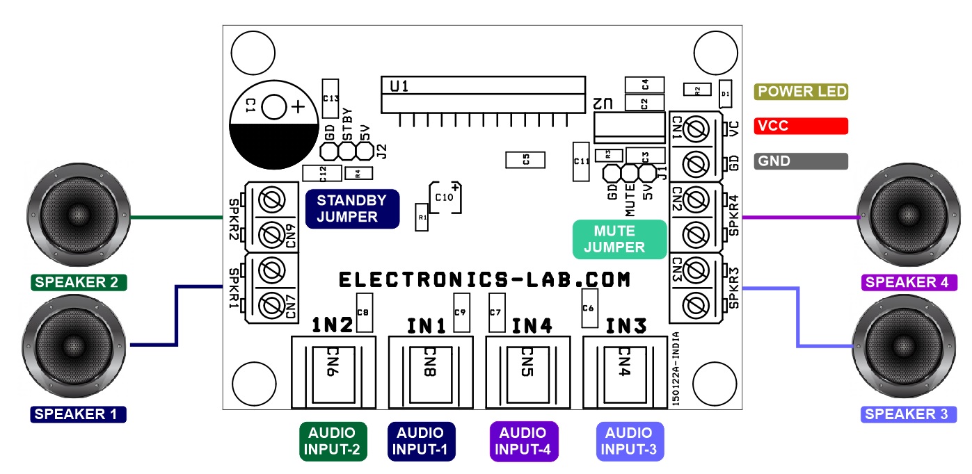
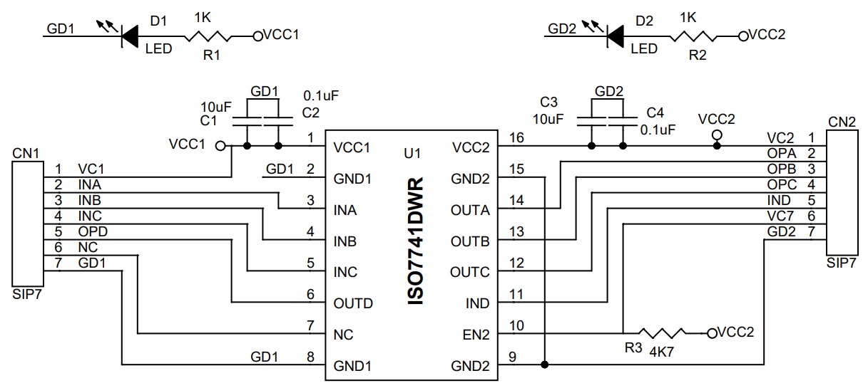
Connections and Other Details
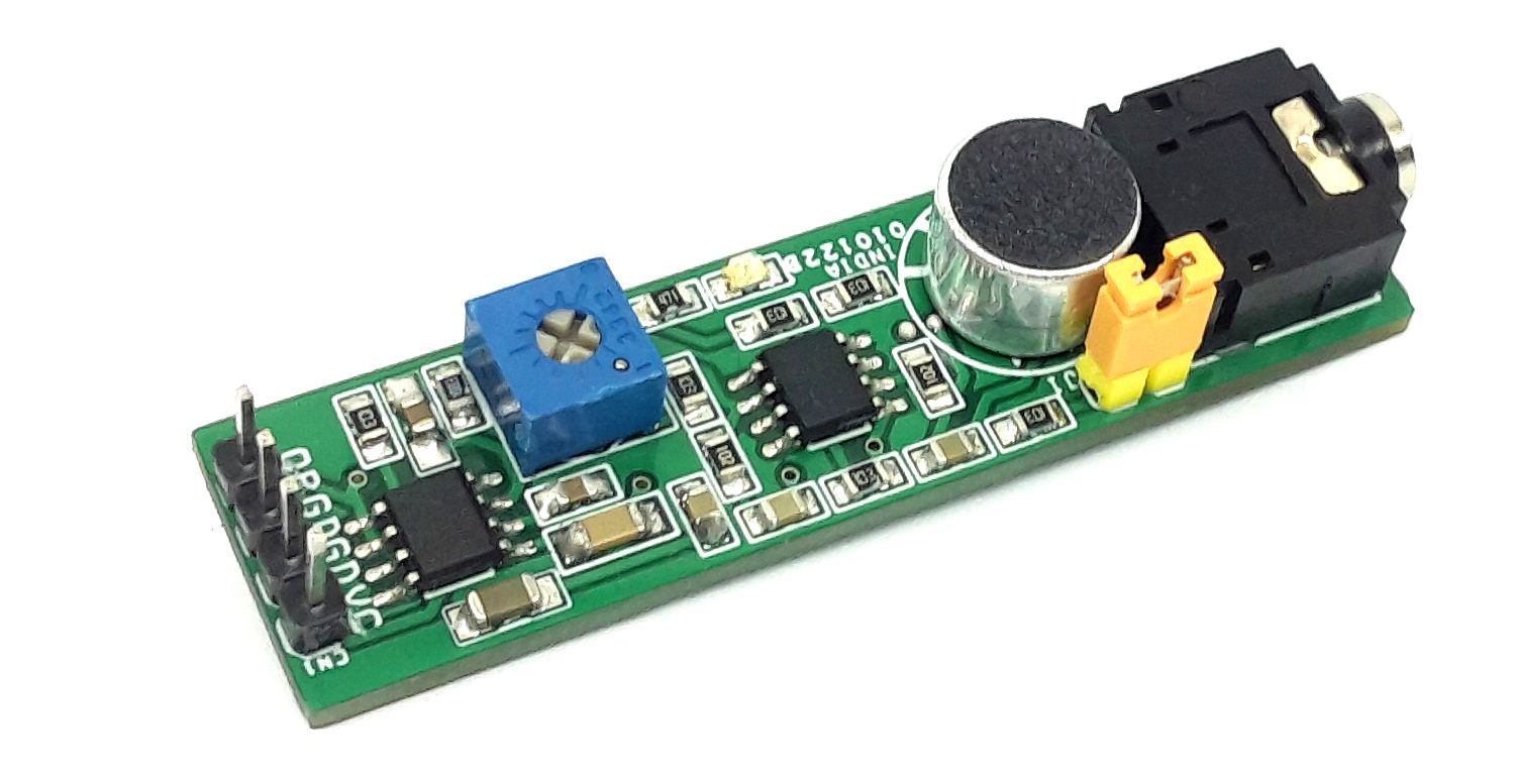
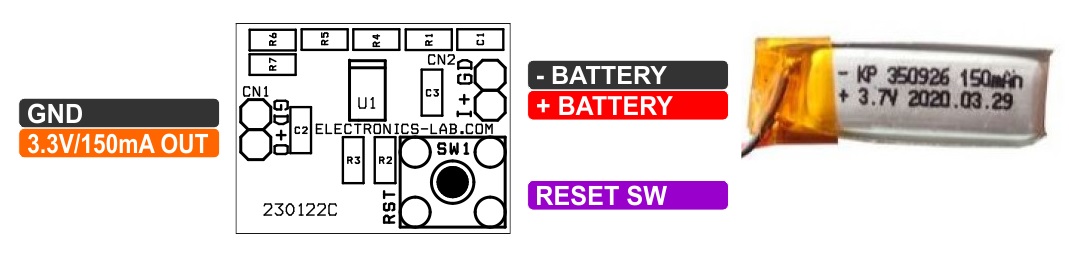
- CN1: Pin 1 +V 3.3V Output, Pin 2 GND
- CN2: Pin 1 -Battery (GND), Pin 2 + Battery
- SW1: Reset Switch
Features
- Good for 3.6V Li-Ion Battery
- Output 3.3V @ 150mA
- Cut-off Voltage 3.08V
- Load Up to 150mA
- On Board Reset Switch
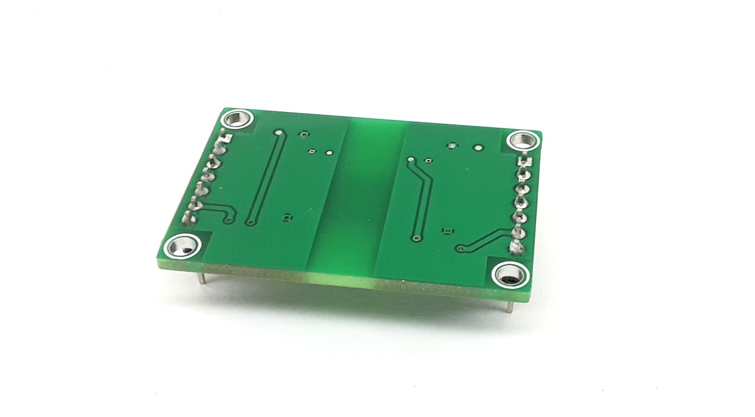
- PCB Dimensions 23.18 x 17.46mm
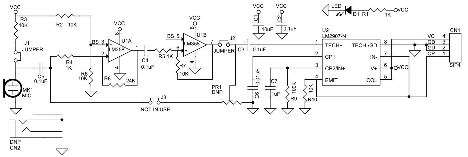
Schematic
Parts List
| NO | QNTY. | REF. | DESC | MANUFACTURER | SUPPLIER | PART NO |
|---|---|---|---|---|---|---|
| 1 | 1 | CN1 | 2 PIN MALE HEADER PITCH 2.54MM | WURTH | DIGIKEY | 732-5315-ND |
| 2 | 1 | CN2 | 2 PIN MALE HEADER PITCH 2.54MM | WURTH | DIGIKEY | 732-5315-ND |
| 3 | 1 | C1 | 1uF/10V SMD SIZE 0805 | YAGEO/MURATA | DIGIKEY | |
| 4 | 2 | C2,C3 | 4.7uF/10V SMD SIZE 0805 | YAGEO/MURATA | DIGIKEY | |
| 5 | 1 | R1 | 220K 5% SMD SIZE 0805 | YAGEO/MURATA | DIGIKEY | |
| 6 | 1 | R2 | 1K 1% SMD SIZE 0805 | YAGEO/MURATA | DIGIKEY | |
| 7 | 2 | R3,R4 | 1M 0.1% SMD SIZE 0805 | YAGEO/MURATA | DIGIKEY | |
| 8 | 1 | R5 | 49.9K 0.1% SMD SIZE 0805 | YAGEO/MURATA | DIGIKEY | |
| 9 | 1 | R6 | 604K 0.1% | YAGEO/MURATA | DIGIKEY | |
| 10 | 1 | R7 | 0E SMD SIZE 0805 | YAGEO/MURATA | DIGIKEY | |
| 11 | 1 | SW1 | TACTILE SWITCH | NKK SWITCH | DIGIKEY | HP0215AFKP2-ND |
| 12 | 1 | U1 | MAX882 SOIC8 | ANALOG DEVICE | DIGIKEY | MAX882CSA+-ND |
Connections
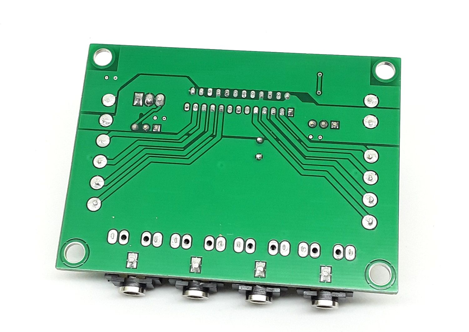
Gerber View
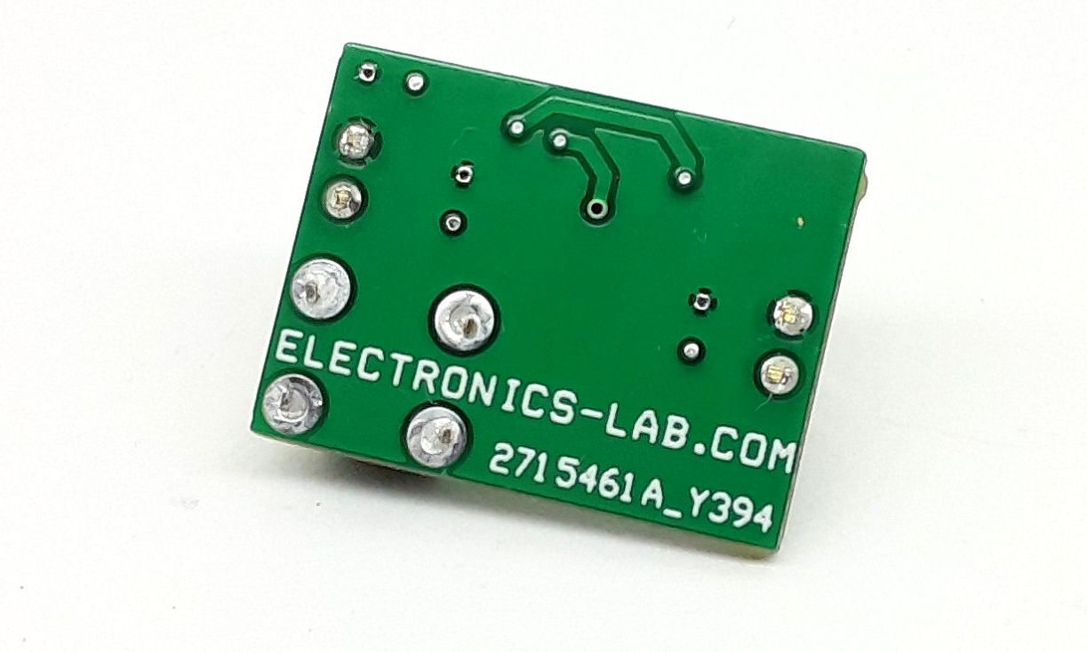
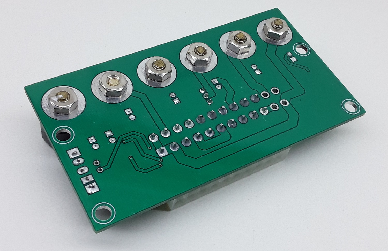
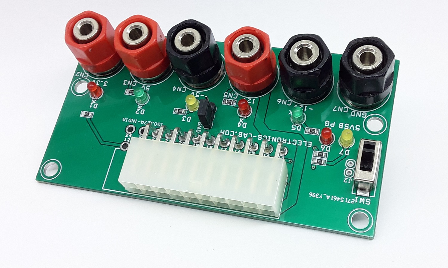
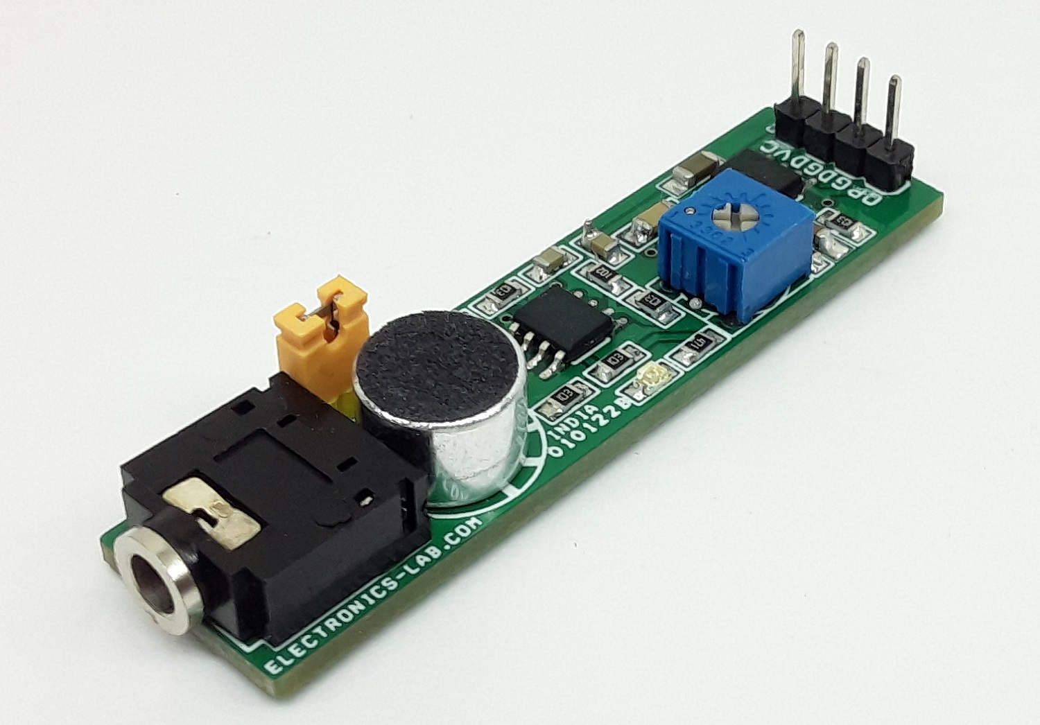
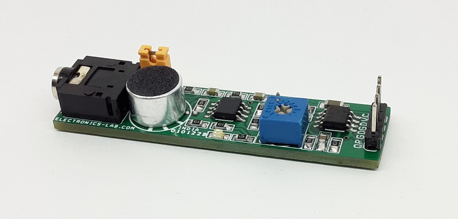
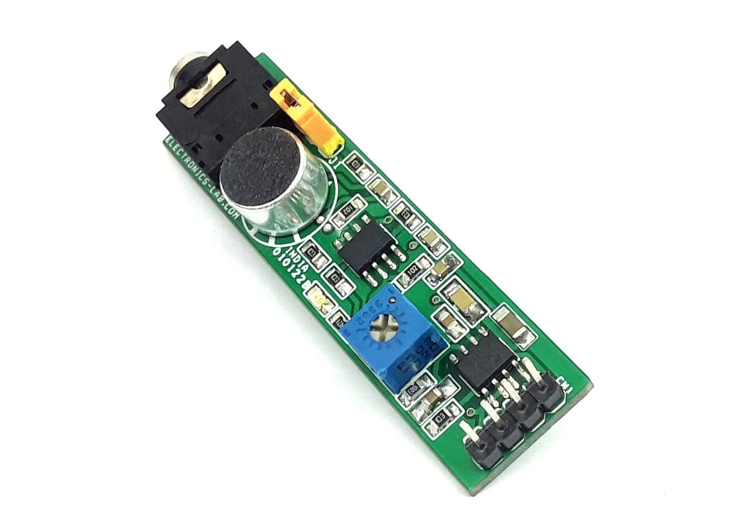
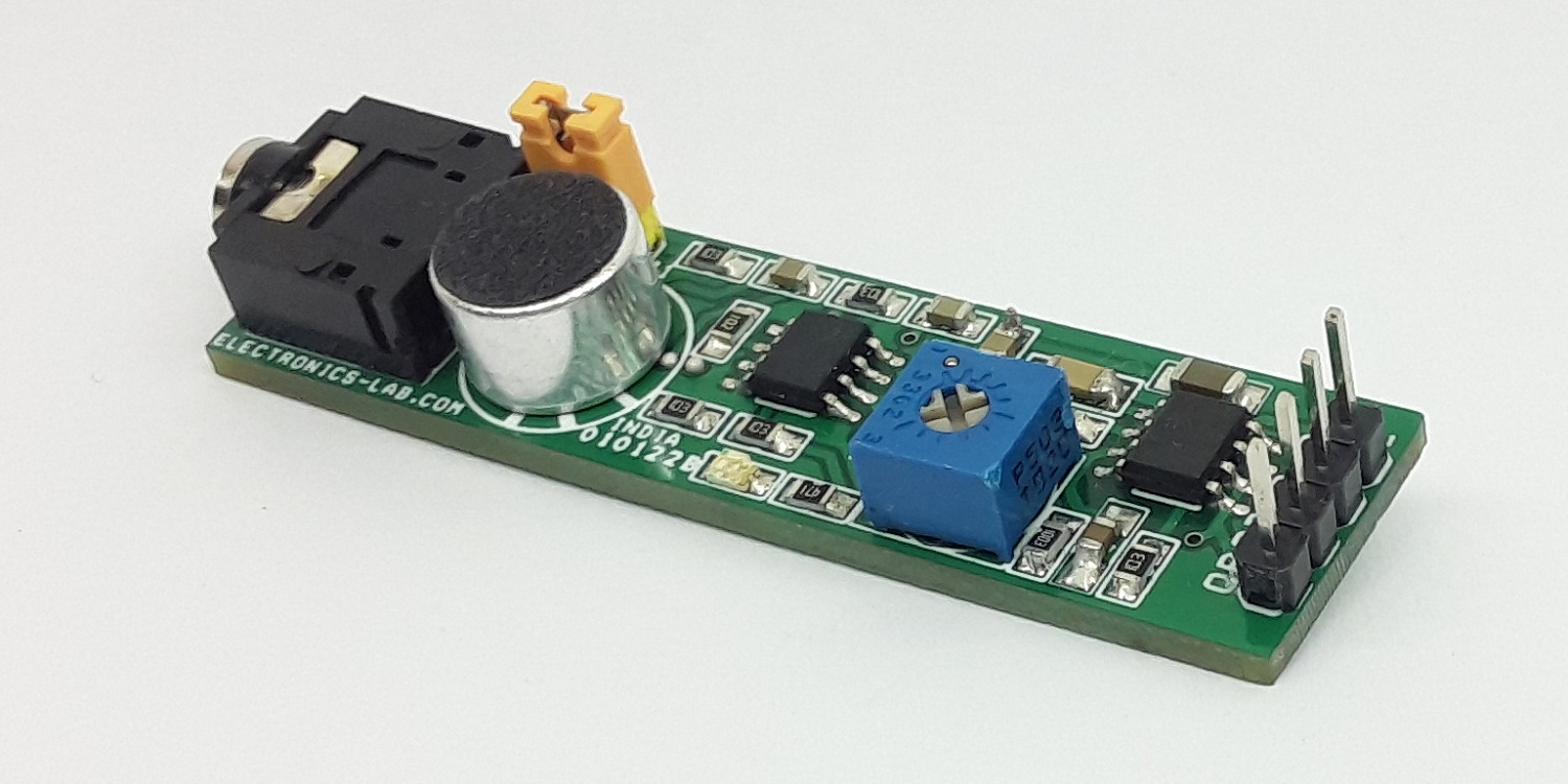
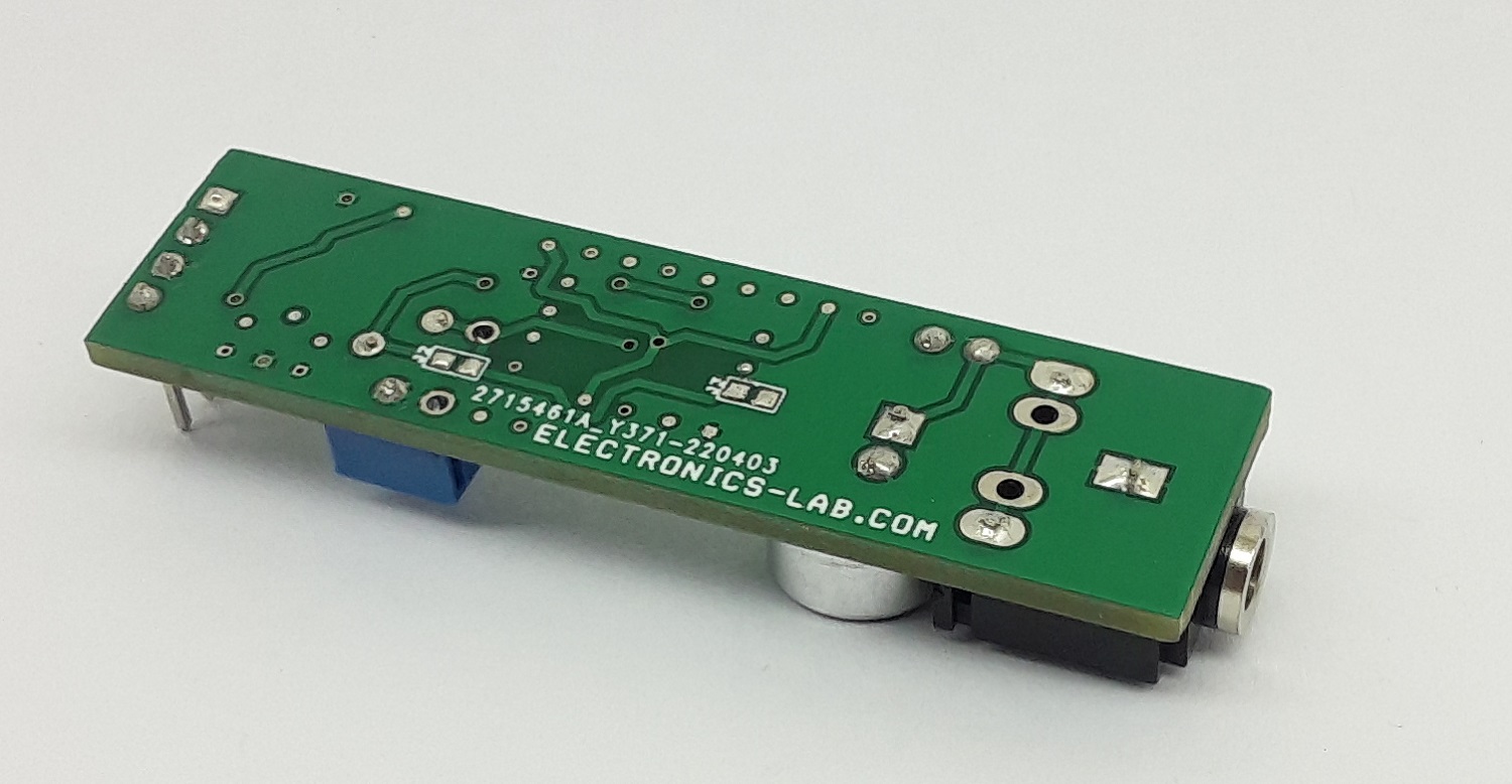
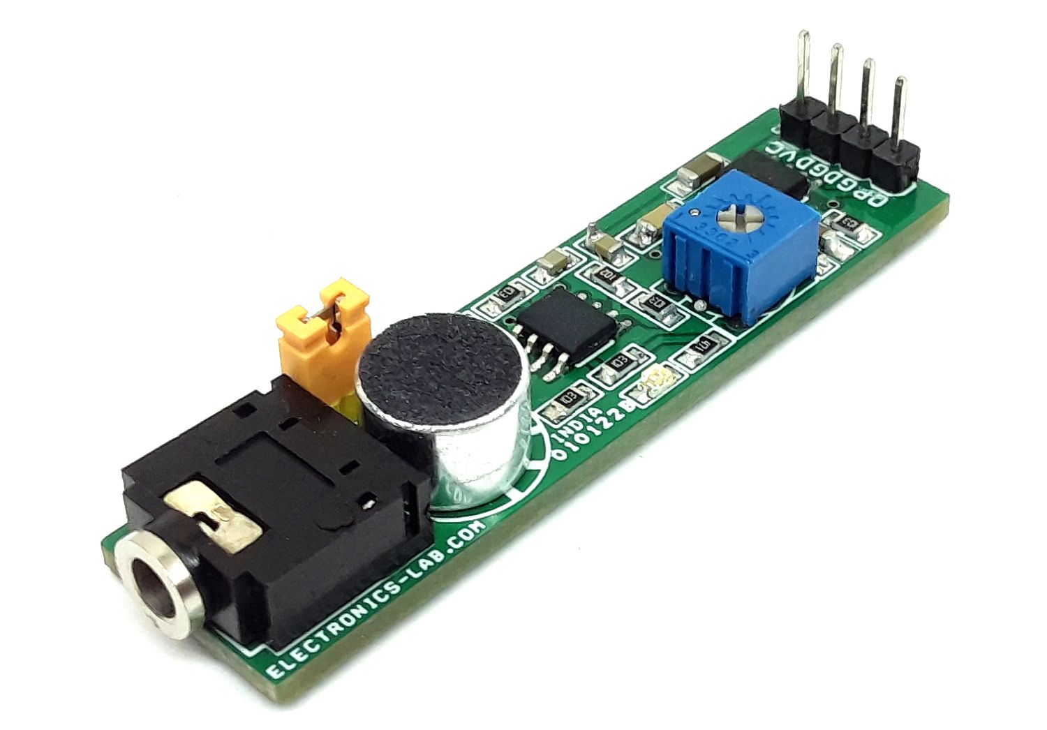
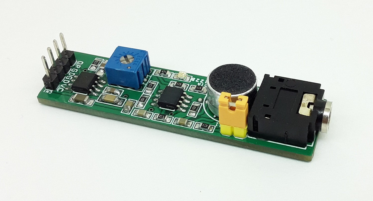
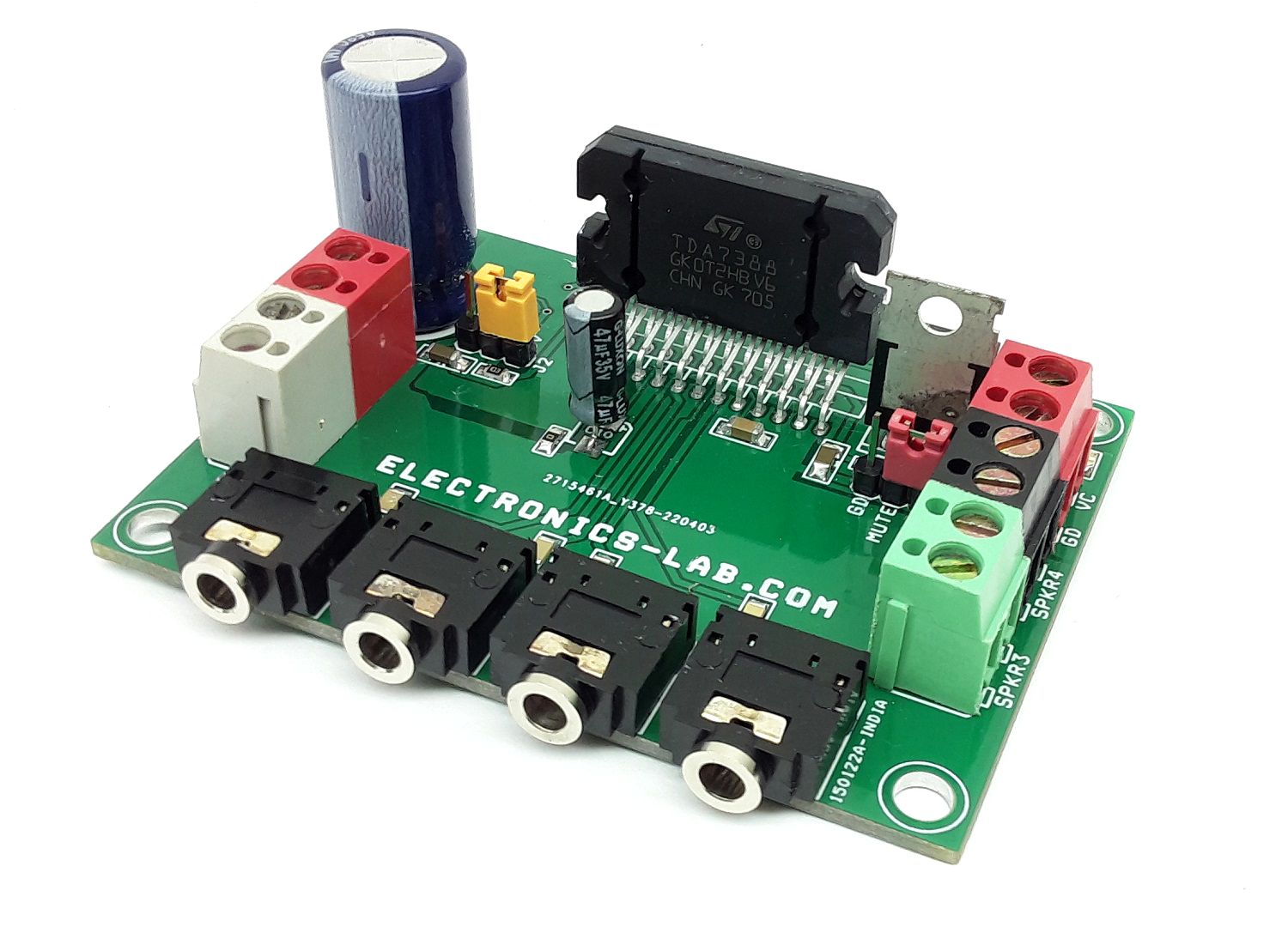
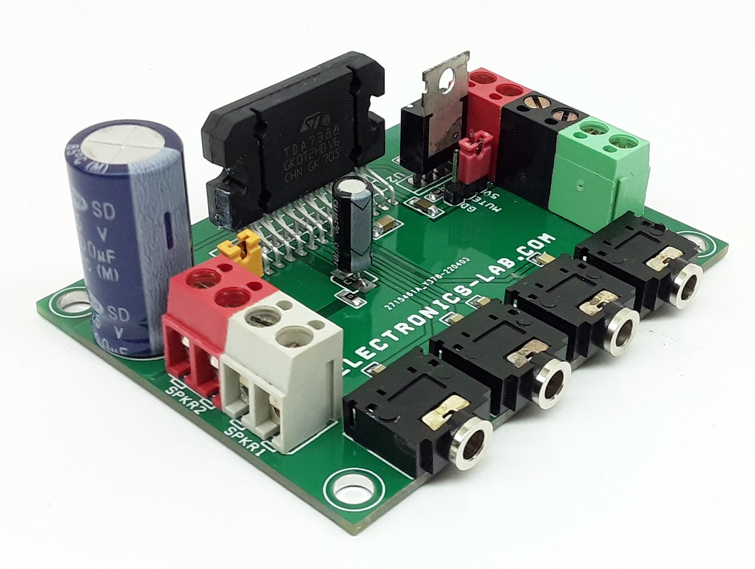
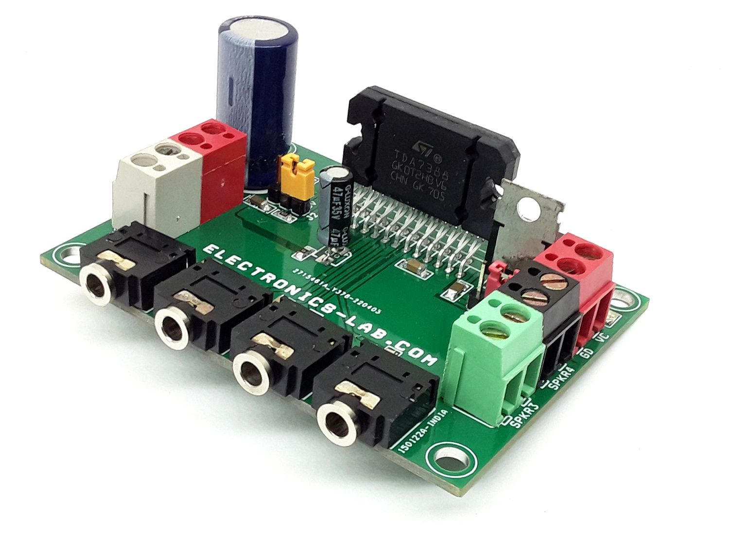
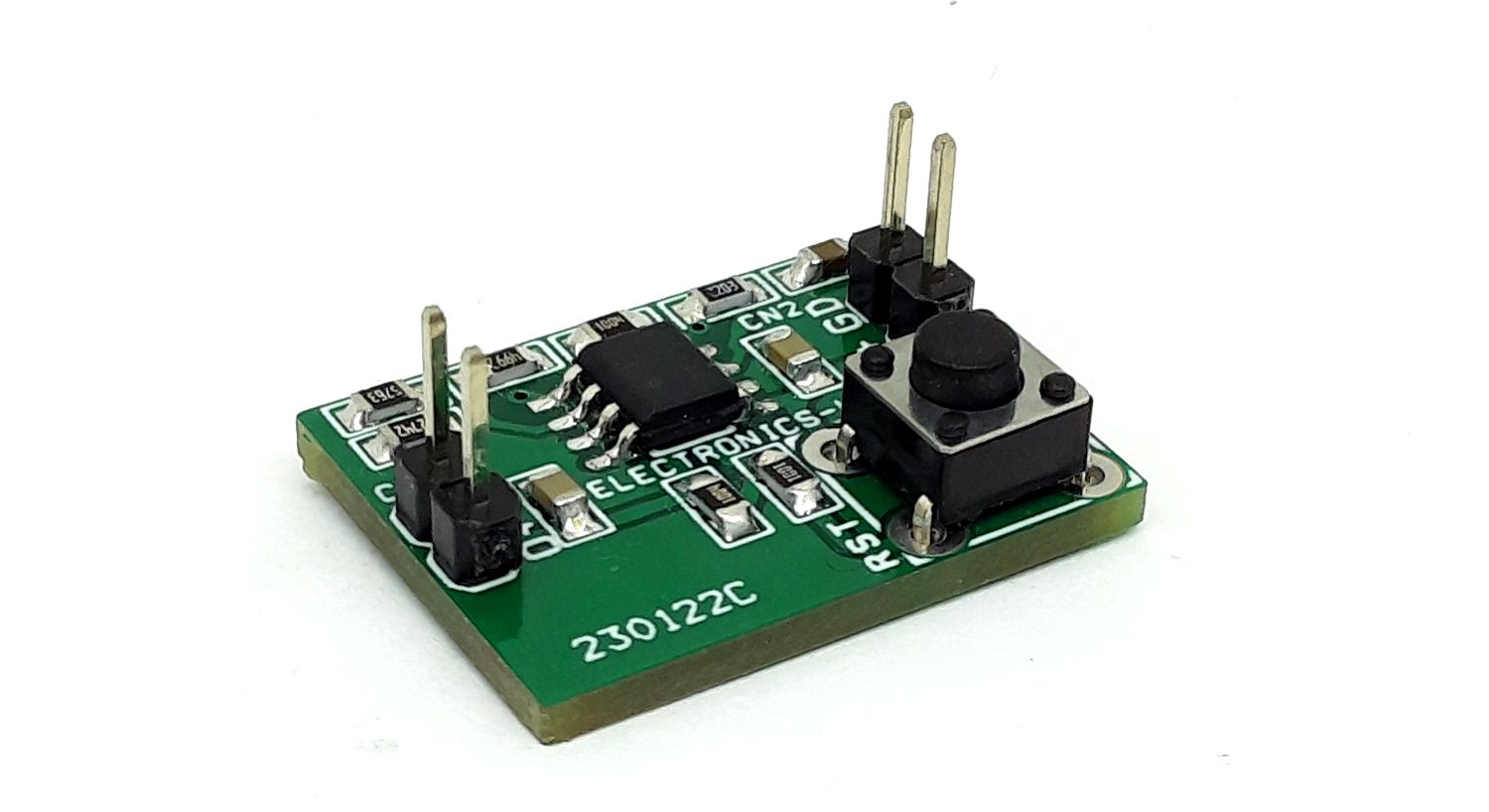
Photos