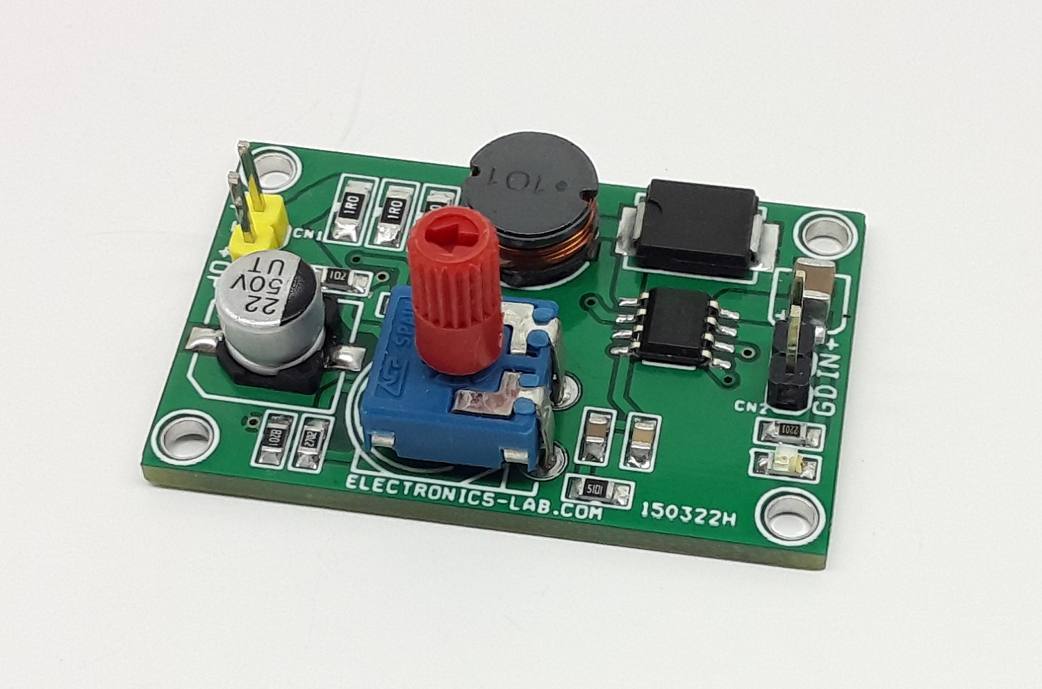
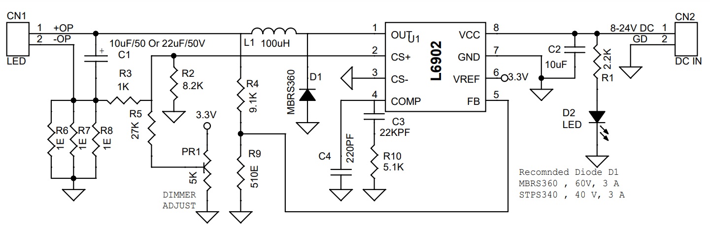
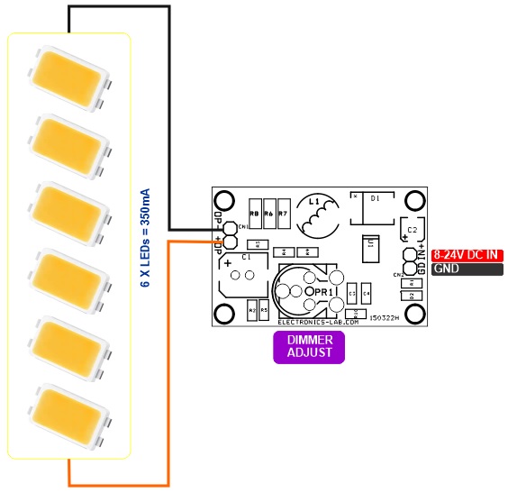
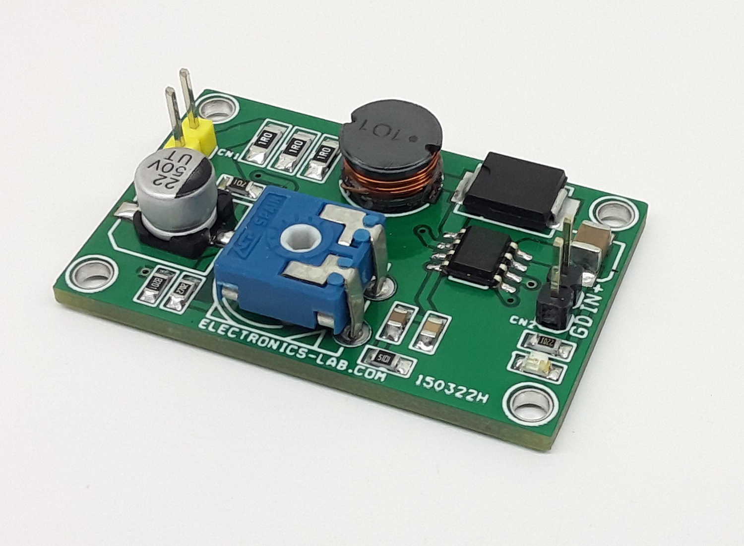
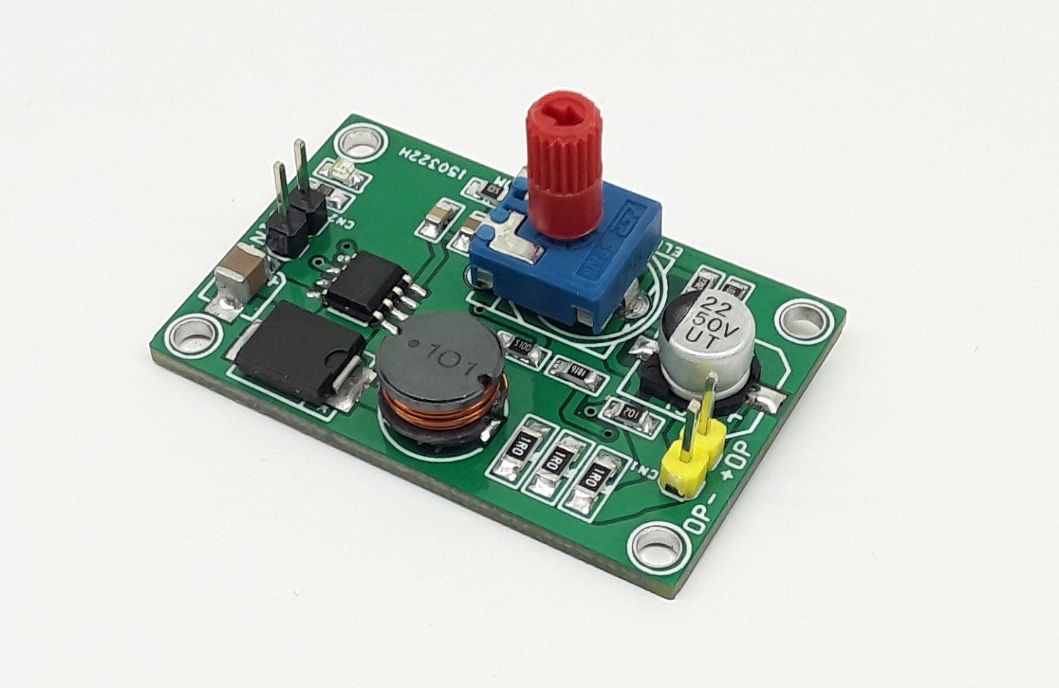
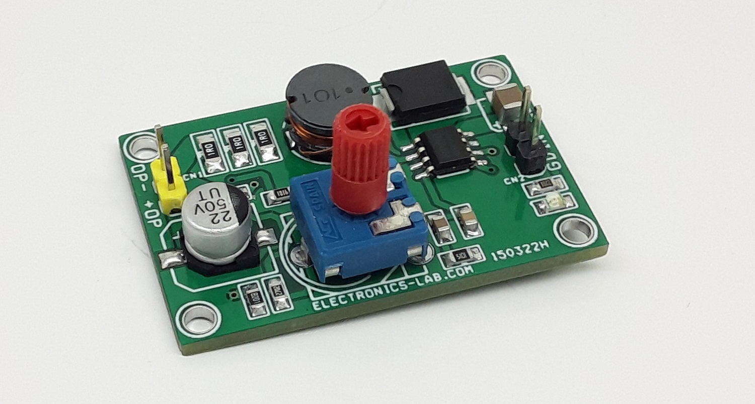
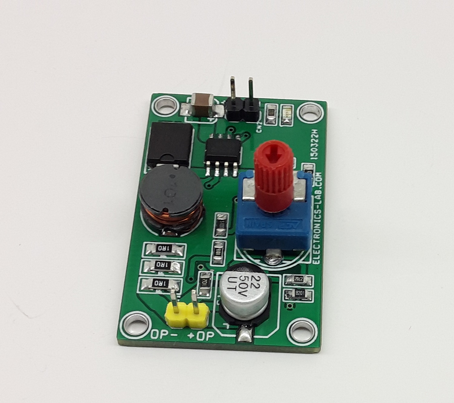
This is a high-efficiency and reliability DC/DC converter with a dimming feature for super high brightness LEDs. The project is built using L6902D chip. L6902 is a complete and simple step-down switching regulator with adjustable current limit. The current control loop with external sense resistors R6, R7, and R8 are able to work in constant current mode providing up to 350mA output current with an accuracy of 5%. Potentiometer PR1 helps to control the dimming of the LEDs. PR1 is connected to the 3.3V reference pin of the chip. When the dimming (CS+) pin is grounded (0V) the maximum output current is provided (350mA) and vice versa when 3.3V is applied to the pin, the current provided is zero and so the LED is off.
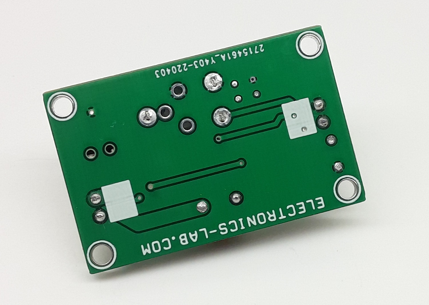
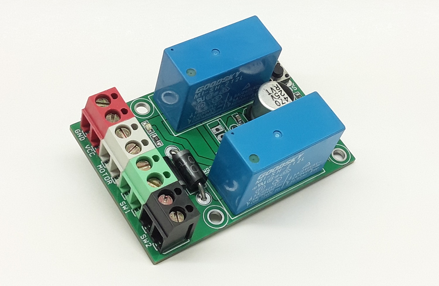
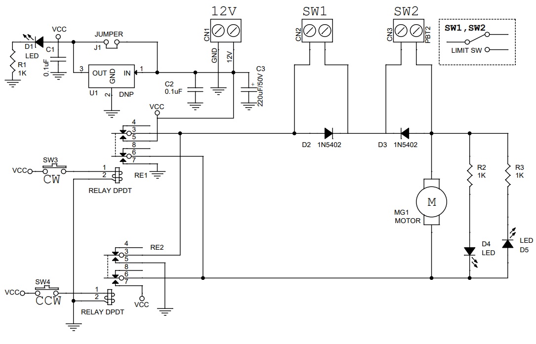
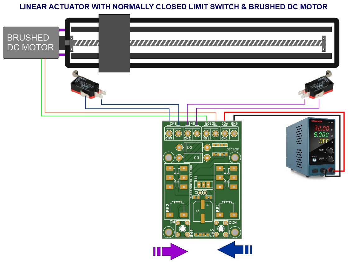
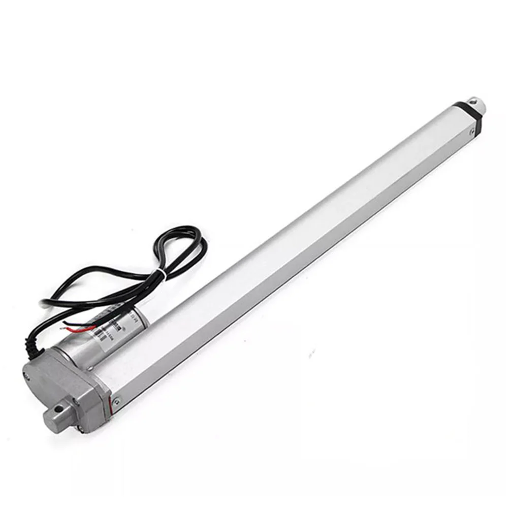
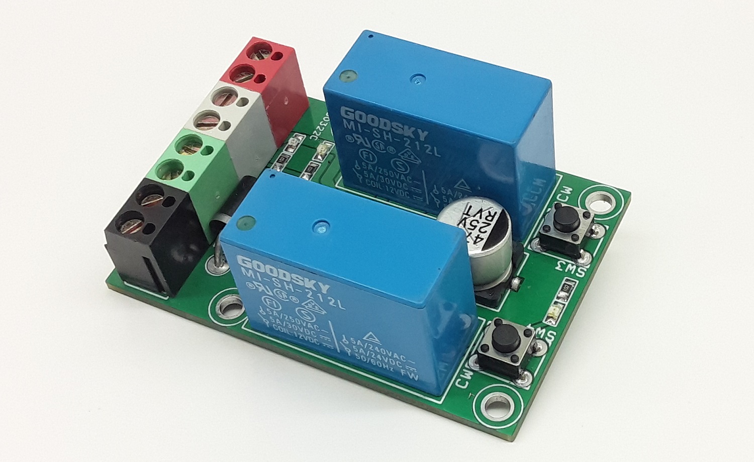
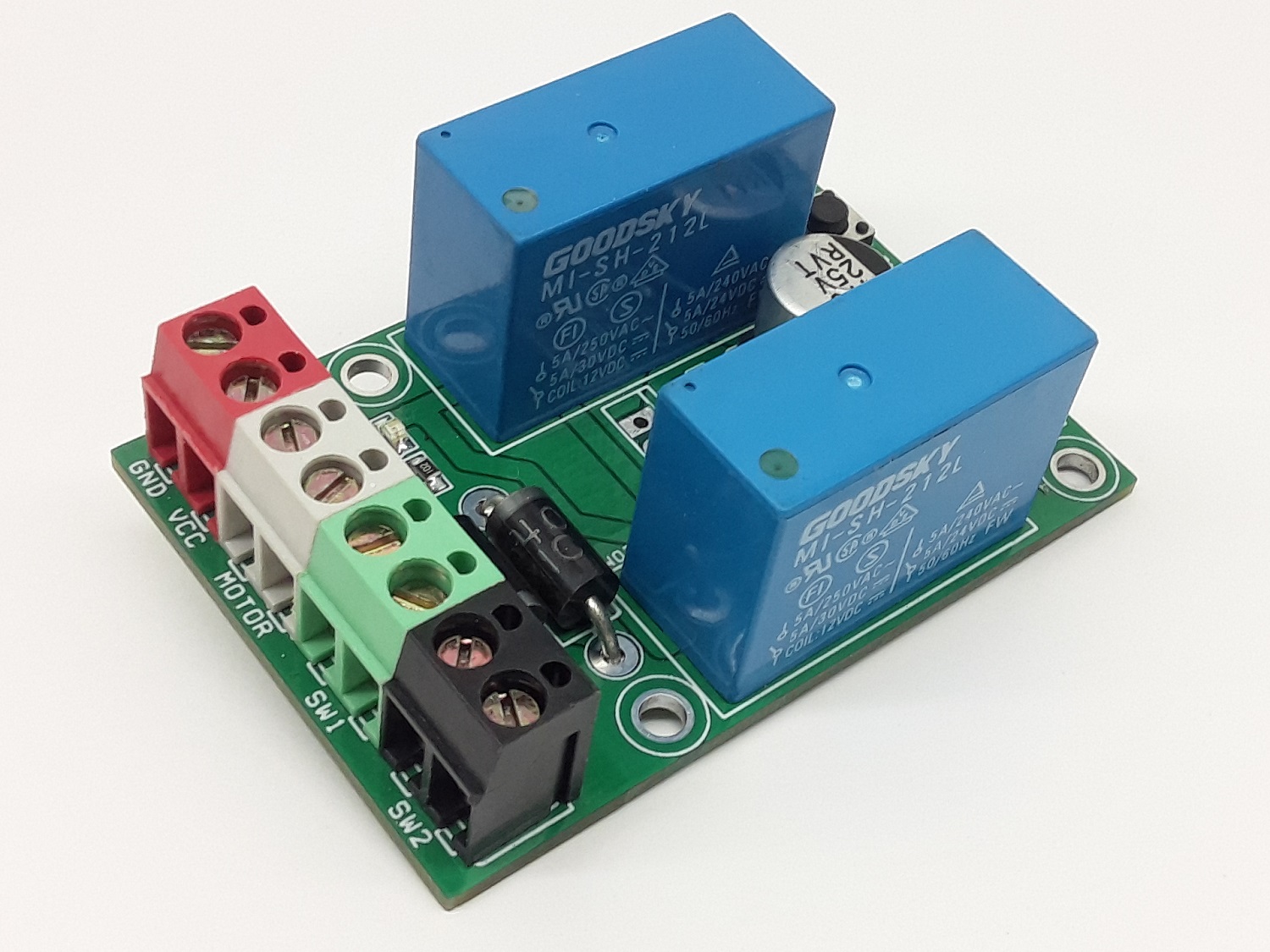
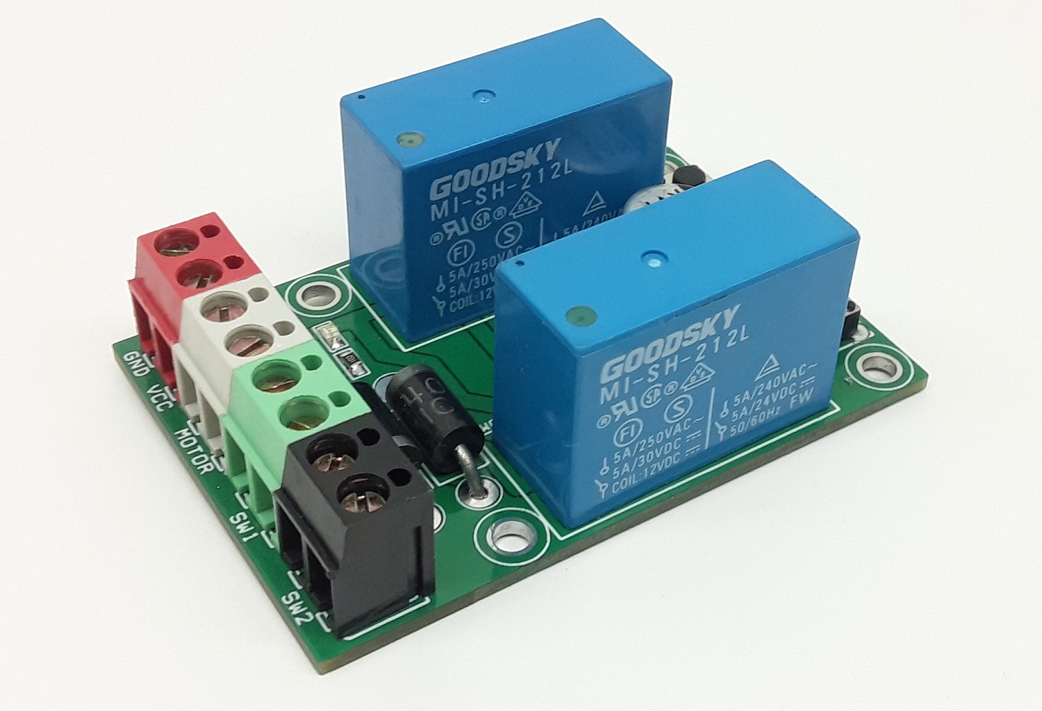
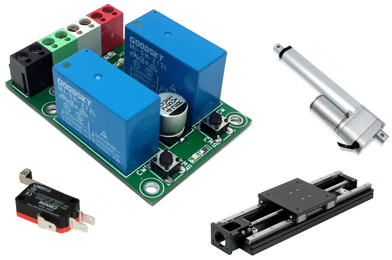
The project described here is a very useful device for use with linear actuators. This controller prevents the actuator from reaching the physical movement limits of the actuator, thus it prevents burnout of motor and physical/mechanical damage to the actuator itself to the mechanical machine associated with it. It also allows for a smoother stopping motion once the end of travel is reached. The project is capable to drive DC brushed motor up to 3A, it supports 12V DC or 24V DC motors with few changes. Two limit switches are used on both sides of the actuator. The limit switches are available with 2 contacts normally open and normally closed. It is advisable to use normally closed contacts. The project consists of 2 DPDT relays, two 1N5402 diodes, Power LED, Motor direction LEDs, 2 x tactile switches, DC supply capacitor, screw terminals, etc.
Operation
Make all the connections as per the diagram, and install the limit switches at the end of the actuator. It is important to provide little offset space for motor movement. Power the board. Press any of the tactile switches SW1 or Sw2, actuator starts moving in one direction, once it hit the end limit switch, the switch is open, and the diode which is connected across the switch stops the current flow in that direction, and the motor stops. Now press the other switch, in this case, the current flow is reversed and the associated diode allows the motor to run in reverse directions and continue till it hit the other side of the limit switch. It is important to check the motor direction as per diode polarity, and swap the motor connections if the system doesn’t work properly or misbehaves.
The controller can drive 12V or 24V Motor (Maximum Current 3A)
12V DC Motor
Do Not Use Regulator U1, Jumper J1 closed, rest components as per schematic.
24V DC Motor
Open the Jumper J1
Resistor Value R1, R2, and R3 = 2.2K Ohms
Install U1 Regulator LM7812
In the case of a 24V Relay, don’t install the regulator, and use jumper J1.
Note: It is advisable to use an appropriate high current limit switch, as it should be able to handle the high current of the DC Motor, considering the peak current of the motor.
Features
Motor Supply 12V DC (for 24V Motor Read Note)
Maximum Load Current 3A
2 x Tactile switch to drive Motor in CW/CCW
2 x LEDs for Motor Direction
On-Board Power LED
Screw Terminals for Motor Connections, Limit Switch, Power Supply
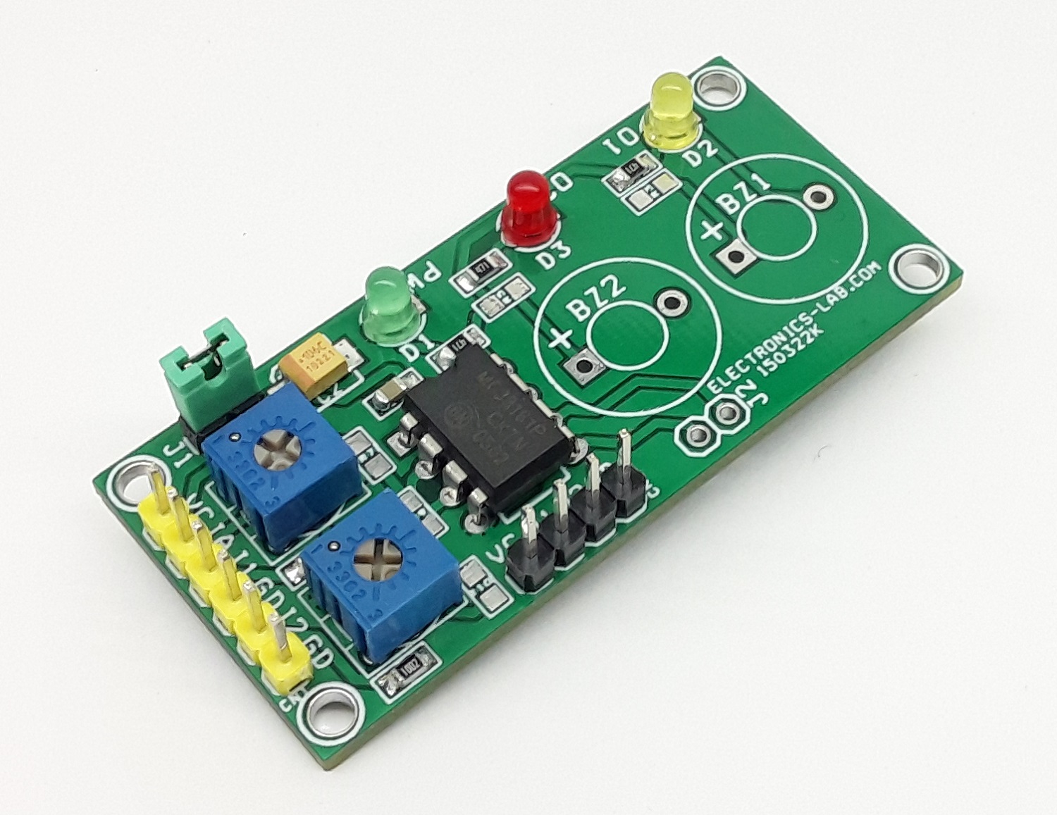
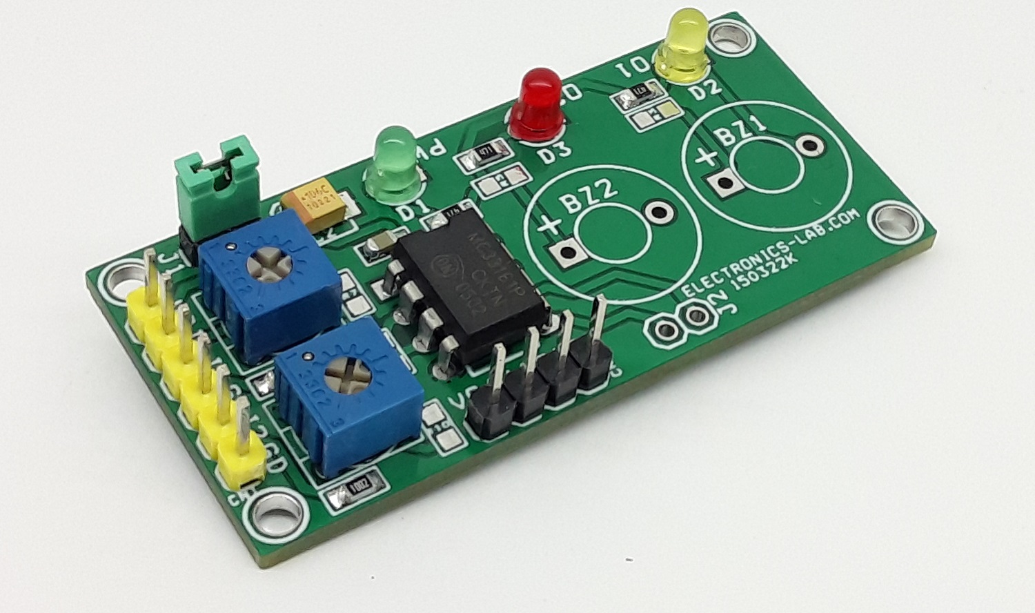
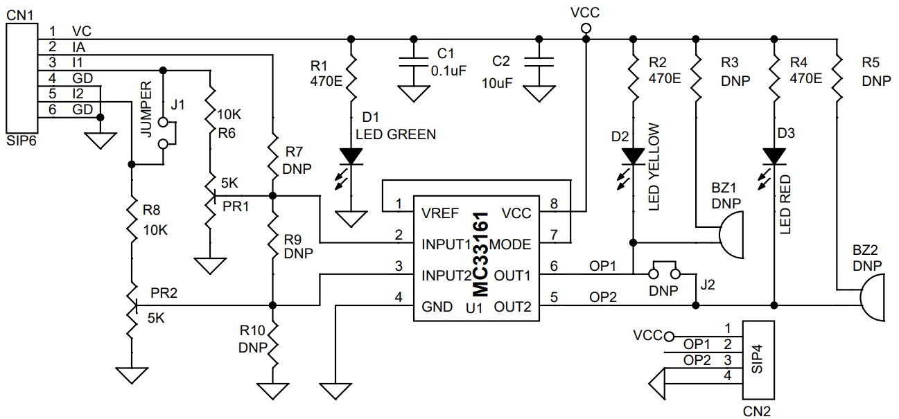
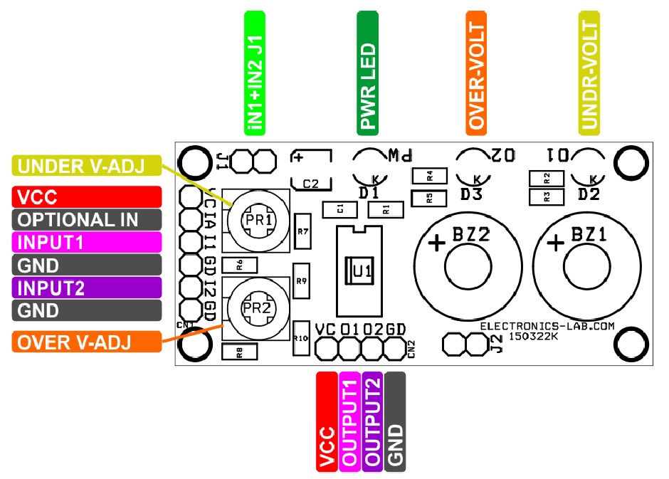
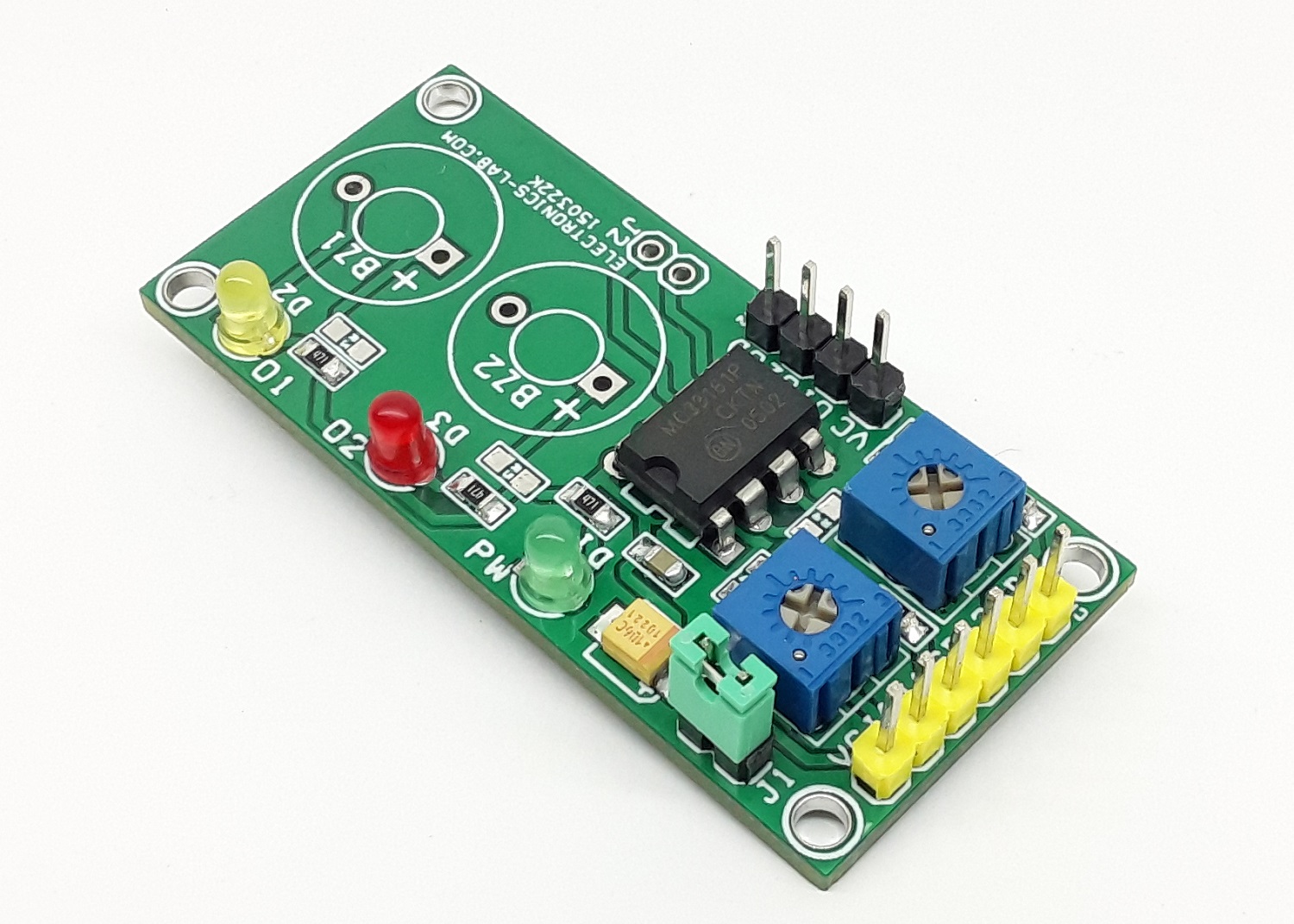
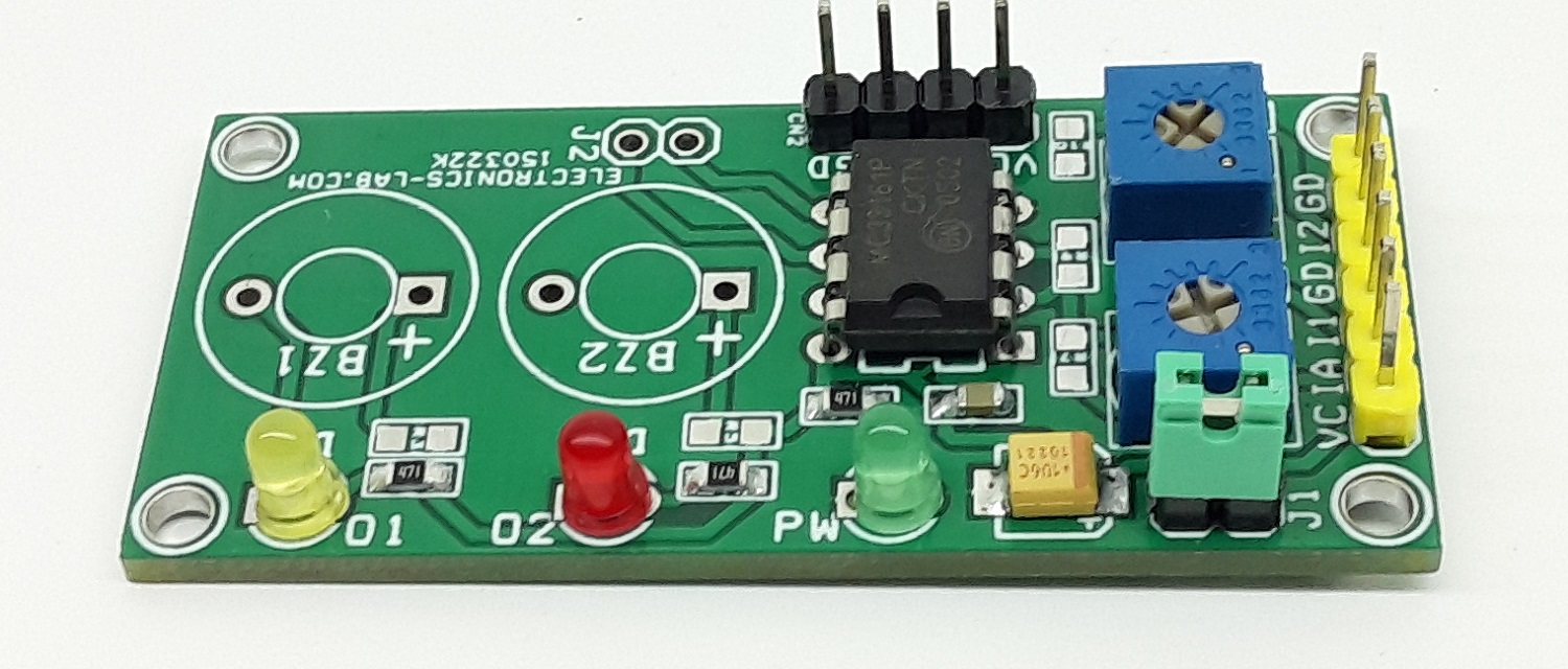
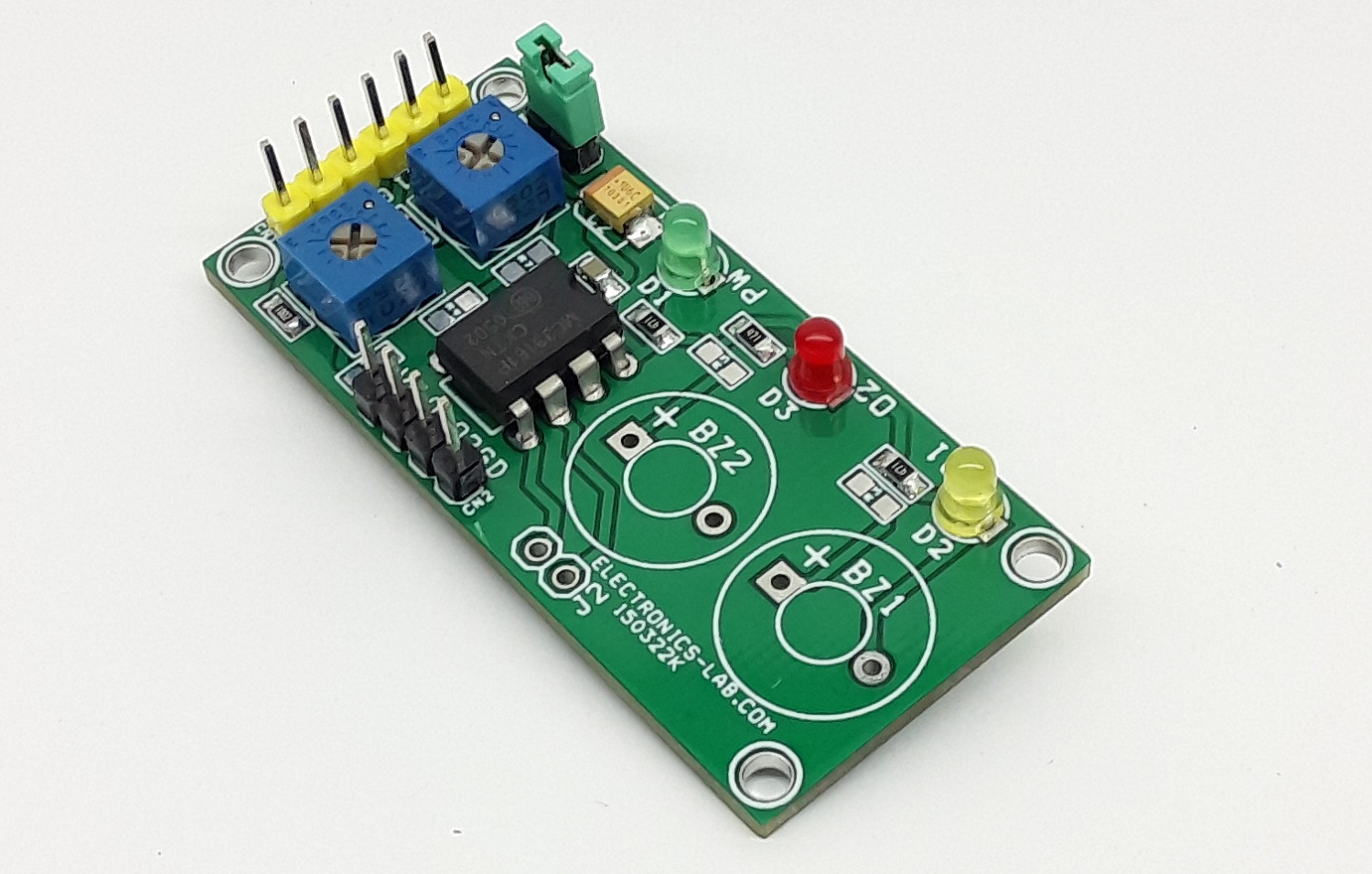
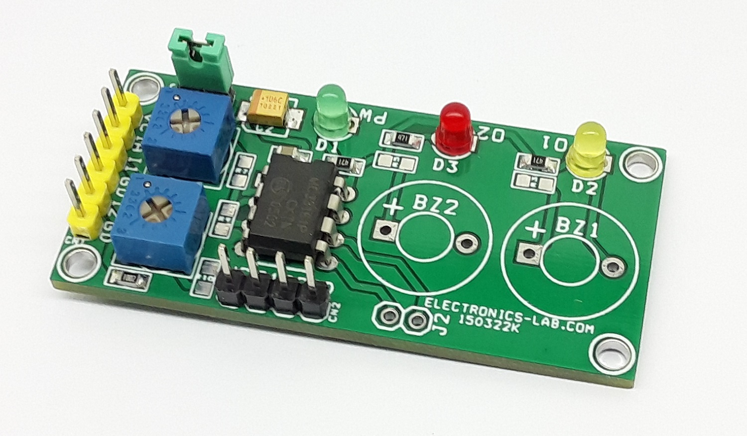
This project is built using MC33161 IC, which is a universal voltage monitor intended to be used in a wide variety of voltage sensing applications. The project offers an economical solution for positive and negative voltage detection. The circuit consists of two comparator channels each with hysteresis, a unique Mode Select Input for channel programming, a pinned out 2.54 V reference, and two open collector outputs installed with LED for visual alert for under-voltage and over-voltage situations. The project is configured for a 5V supply by default. It provides a visual indication when supply is lower the 5V and over 5V. Yellow LED indicates undervoltage and Red LED indicates overvoltage. Trimmer potentiometers PR1 and PR2 were provided to adjust the Undervoltage and Overvoltage range. Both inputs can be used as independent or combined (Single Input)
Note: The board is configured to detect Undervoltage and Overvoltage for 5V Supply, however, it provides the user with multiple choices and extensive flexibility for different applications circuits and configurations. It may be used in many combinations for various options, refer to the datasheet of the chip for various options, following components R7, R9, R10, Jumper J2, Buzzer BZ1-BZ2 provided to implement various circuits.
PR1 Trimmer Potentiometer – Under Voltage Range Adjust
PR2 Trimmer Potentiometer – Over Voltage Range Adjust
Testing the Circuit
Close Jumper J1, Connect the 5V DC power supply to CN1 Pin1 +VC and Pin6 GND. Set the Adjustable power supply to 4.5V DC and connect it to Pin 3 or Pin5 of the CN1 Connector. Turn the PR1 trimmer potentiometer carefully so the Yellow LED glows, now set the adjustable power supply to output 5.5V and turn the trimmer potentiometer PR2 such Red LED D3 should glow. Now, the project is configured and ready to be used. It is set to detect and indicate undervoltage of 4.5V and Over voltage of 5.5V. Connector CN2 can help for microcontroller interface, Output 1 and Output 2 Normally goes High or low when under/over voltage conditions are detected.
Features
Power Supply 5V DC (Range 5 to 12V DC)
Yellow LED for Under Voltage detection
Configured for 5V Detection
Red LED for Overvoltage Detection
Provides Visual Alerts when Under-Over Voltage is Detected at input 1 and Input 2
Output 1 and Output 2 for Micro-Controller Interface
LEDs can be Replaced with Audible Buzzer (Low Current Buzzer 10mA maximum)
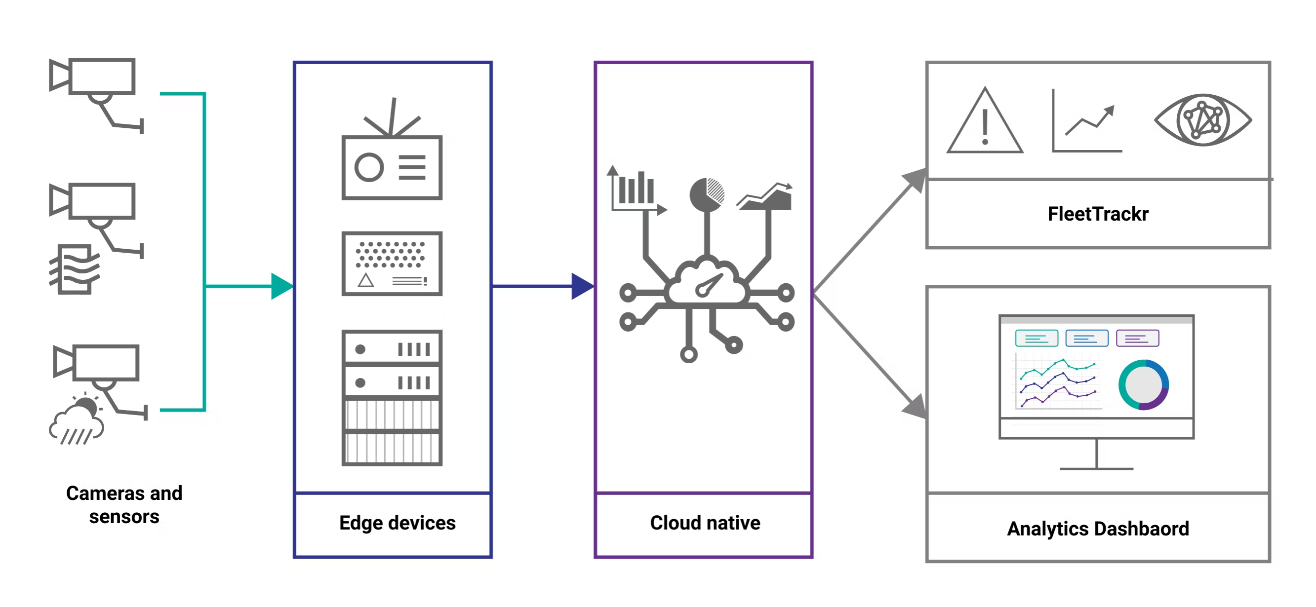
Malta-based AI startup SmartCow has announced the availability of a new AIoT device management platform, FleetTrackr, for simplified deployment and centralized management of edge AI systems. All of this will be done through a unified platform using a hybrid-cloud service, specifically for applications, including smart cities, security, surveillance, and traffic management. This is an essential tool for enterprises where thousands of edge IoT devices are deployed in the edge network.
For enterprise-edge AI applications, thousands of edge sensors are simultaneously transmitting data for processing and real-time response. SmartCow FleetTrackr will be used in such situations where there are several AIoT devices connected for smart manufacturing using AI for inventory management, large-scale surveillance, security deployments, and smart retail automation.
“Fleet management software will revolutionize companies’ ability to digitally transform their business operations, and FleetTrackr is at the forefront of specialty AIoT device management software,” said Ravi Kiran, SmartCow at CEO. “We recognize the need for responsive, flexible, and remotely-operated AI solutions as demand increases for efficient, smart technology.”
One of the concerns of the thousands of edge devices deployed on the edge network is reprogramming and updating these devices. With SmartCow FleetTrackr, there comes Firmware-Over-the-Air (FOTA) functionality, which allows the user to manage, monitor, and update edge devices over the air. FleetTrackr’s24×7 remote management also includes security and privacy features with a 30% reduction in maintenance, time, and labor costs.
There are several key features provided by the company, but some of the important ones, include device lifecycle management, Firmware-Over-The-Air updates, predictive maintenance capabilities, issue management, Out-Of-Band functionality, and support for multiple IT environments. The Out-Of-Band functionality gives you the flexibility to remotely send updates to your device and allows firmware backup and recovery whenever the device goes wrong.
“FleetTrackr allows administrators to update all the devices in the desired network with new software without spending weeks planning and executing deployment plans,” continued Kiran. “FleetTrackr enables users to not only identify problems with large fleets of devices, but to perform software updates as well as backup and restore firmware when a device turns out to be faulty, making the experience seamless, efficient, and secure.”
SmartCow recently introduced the Apollo development kit integrated with the Jetson Xavier NX supercomputer. The SmartCow Apollo development platform is equipped with onboard sensors, such as four microphones, two speaker terminals, two 3.5mm phone jacks, an 8MP IMX179 camera module, and an OLED display.
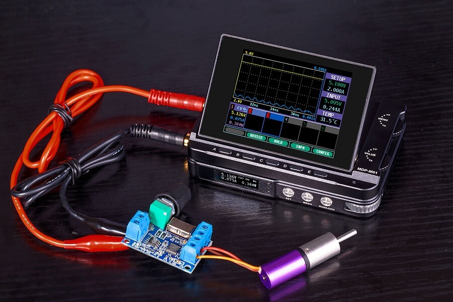
Miniware is one of the versatile technical service companies that has introduced its programmable linear DC power supply, MDP-XP. During the interfacing procedure, this MDP-XP (Mini Digital Power Supply) can link numerous devices at the same time. With MDP-XP’s modular design, it enables you to improve the fundamental capabilities of a device. Along with its unique user interface, it is a low-cost, reliable, and stable DC power supply. An STM32 smart chip controls this MDP-XP, allowing the users to customize the parameters and upgrade the firmware at any time. It includes a Display Control Module (MDP-M01) and a Digital Power Module (MDP-P905).
MDP-M01 Display Control
With the MDP-M01 Display Control, you get a quick and easy-to-learn interface that enhances the user experience. Equipped with a 2.8-inch 90° flipping TFT screen, it has the potential to display the real-time voltage/current waveform. It also supports data statistics, and automatically pairs and controls 6 sub-modules or the display power modules. This Display Control features dual thumb wheels which consist of a value wheel and the menu wheel. The value wheel controls the adjusting values whereas the menu wheel can be utilised for selecting the options.
MDP-P905 Digital Power Module
On the other hand, the MDP-P905 Digital Power Module provides a high-efficient linear output of up to 95% with 0.25mV ultra-low ripple. This Power Module delivers a 4µs high transient response along with precise fine-tuning of 0.001V and 0.001A. The 4MM high-quality copper interface plays a big role in providing protection against high current corrosion. The DC input voltage range is between 4.2V and 30V, which further reduces to 2.7V after startup, meanwhile, the output voltage is 30v/5A.
Features of MDP-XP
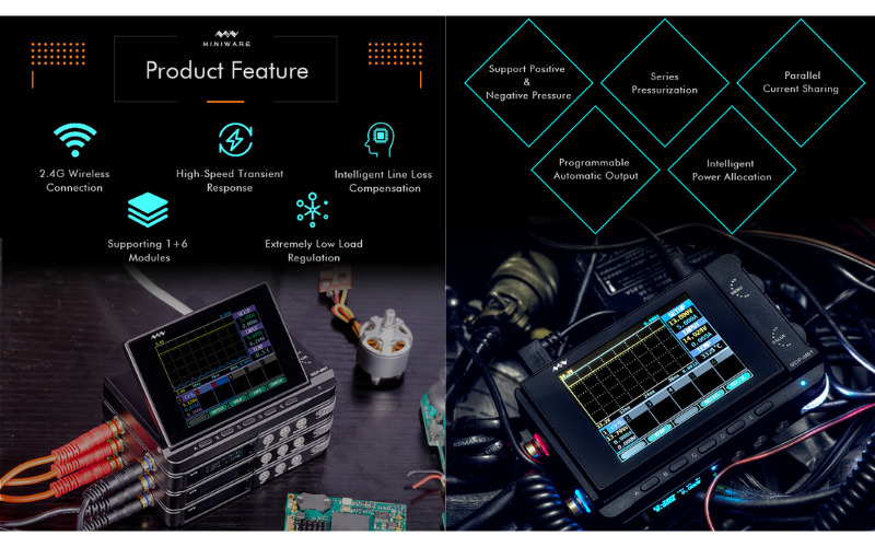
A wireless connection of 2.4G makes it possible to achieve a multichannel combination at the power of 90W per channel. This wireless connection supports the Display Control, as well as the six Digital Power Modules.
The low load regulation contributes to the accurate power supply. On the other hand, the intelligent line loss compensation ranging from 5mR to 100mR results in tremendous power transfer.
In addition to presenting precise waveforms, this software can save data up to 7MB with a maximum recording limit of 24 hours. The load and the power adjustment rates are <±0.01^% and it also supports Qualcomm’s quick QC3.0 port.
In addition to its high cost-effective programmable linear DC power supply, it is necessary to consider the safety parameters too. Hence, MDP-XP offers 6 safety protections, including input overvoltage, under-voltage, anti-reverse connection, anti-backflow, overtemperature, and overcurrent.
The programmable output, timing output, sequential control, automatic compensation, and other innovative features fulfil a huge spectrum of testing requirements.
This high power supply unit can be used in R&D laboratories for universal testing and teaching experiments, maintenance of digital devices, testing of power supplies in devices, or to provide refined power for digital-analog hybrid circuits which have high accuracy and for devices that deliver Hi-Fi audio and for more applications and detailed specification visit the product page.
The smart MDP-XP Digital Power Supply kit is available at a price of just $210.00. With this price, you get an MDP-M01 display module, an MDP-P905 power module, a 2.5mm Audio to Micro USB Cable for data, and two 4mm Banana Plug to Alligator Clip output cables, a 2.5mm Audio to USB Type-A cable, and a user manual. For more information about this product visit Dfrobot’s official website.
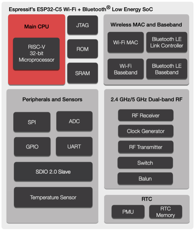
One of the very famous embedded SoC designers and manufacturers, Espressif, has recently announced the launch of yet another 32-bit microcontroller– ESP32-C5 featuring its first dual-band Wi-Fi solution. As the company claims, the ESP32-C5 system-on-chip is a follow-up module to the ESP32-C6 SoC which was announced last year. ESP32-C6 came with the support for Wi-Fi 6 and Bluetooth 5 Low Energy wireless connectivity which was an upgrade from ESP32-C3 SoC. The new ESP32-C5 SoC has an integrated MCU of 2.4GHz and 5GHz dual-band Wi-Fi 6 along with Bluetooth 5 Low Energy connectivity.
The ESP32-C5 SoC is equipped with dual-band Wi-Fi 6 (IEEE 802.11ax) radio and IEEE 802.11b/g/n standard for back compatibility. Wi-Fi 6 support has been an important parameter for its adoption due to its optimized performance for edge IoT devices. The SoC supports 20MHz bandwidth for IEEE 802.11ax mode and an optional 20/40MHz bandwidth for standard IEEE 802.11b/g/n modes.
At the heart of the ESP32-C5 is the 32-bit RISC-V single-core processor that can be clocked up to a frequency of 240MHz. The hardware comes with a 400kB of SRAM and 384kB ROM with support for external flash storage. There are 20 programmable GPIOs that support commonly used peripherals that allow the user to interface camera and display modules. The module also incorporates SDIO 2.0 Slave interface.
“The ESP32 SDIO Card peripherals (Host, Slave) share two sets of pins as below table. The first set is usually occupied by the SPI0 bus, which is responsible for the SPI flash holding the code to run. This means SDIO slave driver can only run on the second set of pins while SDIO host is not using it.”
Enterprise customers who deploy thousands of edge devices into the edge network are looking for low latency and stable connectivity using the 5GHz band. Espressif ESP32-C5 SoC will provide robust wireless connectivity across this spectrum for less traffic and lower interference for mission-critical applications. Wi-Fi 6 is supported by ESP32-C5 and comes with several upgraded features to provide benefits for edge devices. An example taken by the company is the support for the OFDMA mechanism for uplink and downlink communication along with MU-MIMO capacity for download. This feature is a key highlight of the hardware as it improves efficiency and provides low latency communication even in a congested wireless environment.
On the software side, Espressif ESP32-C5 can be used on Espressif’s open-source ESP-IDF suite, which already powers other ESP modules. Due to its robust wireless connectivity, several customers might want to use ESP32-C5 as a communication co-processor with an external host, for which the company has provided ESP-AT and ESP-hosted SDKs. For more information on the Espressif ESP32-C5, visit the official press release.
In 2021, Imagination Technologies revealed that it was developing multiple processors based on Catapult’s open RISC-V architecture. IMG RTXM-2200, a 32-bit RISC-V real-time embedded CPU core, is the first addition to the Catapult family introduced by the firm. The latest news found the IMG RTXM-2200 processor is proposed to focus on real-time computing in sensors, storage controllers, and networking solutions. The all-new design is a 32-bit embedded solution with a wealth of features that can be adapted to a number of high-volume applications.
“We are excited to announce IMG RTXM-2200, our first real-time RISC-V CPU, which underpins our continued commitment to driving growth for the RISC-V ecosystem. Imagination now has a unique and broad portfolio of computing IPs, including GPU, AI accelerators, and now CPU, designed for this innovative architecture”, says Chris Porthouse, Chief Product Officer of Imagination.
The new core is highly scalable and offers Level 1 cache sizes of up to 128 KB for reliable performance, as well as up to 128 KB of tightly coupled memory (both instruction and data). The architecture provides several floating-point formats, such as single-precision and the BFloat16 format for compact AI frameworks, and a RISC-V Bit Manipulation extension to improve code density. Thereby, manufacturers can deploy AI applications through this core without needing an extra chip, which reduces silicon space and enables a more optimized and cost-effective design for AI cameras and smart metering applications. The company has also disclosed an optional interrupt module, debug module, breakpoint triggers, and trace systems for development and debugging.
“RISC-V International is excited to witness Imagination maintaining its momentum by launching its first licensable 32-bit embedded real-time processor since the announcement of its entry into the RISC-V CPU IP market”, said Calista Redmond, CEO of RISC-V International. “This underlines the expansion of the RISC-V architecture as developers take advantage of this flexible technology to address multiple market requirements. We are pleased to see Imagination’s commitment to driving ecosystem growth with the delivery of its SDK and the support of open-source operating systems.”
Imagination claims that it will offer extensive support for software development kits (SDKs) in addition to compatibility with both Linux-based and FreeRTOS real-time operating systems. Catapult Studio Integrated Development Environment is a cutting-edge IDE built on Visual Studio code that provides a familiar environment for modern developers and designers. IDE supports all Linux distributions and is compatible with Windows, Ubuntu, CentOS, and macOS. To simulate power consumption and energy efficiency, it is also compatible with gem5 software.
More details on the RISC-V CPU are available on Imagination’s official product page and in the press release. However, there are no details on the pricing yet.
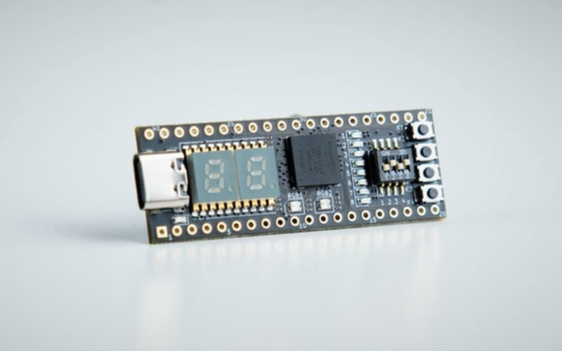
A Chinese tech company in partnership with EIM Technology has announced its STEPFPGA series, which includes the MXO2Core board. Beginners to the field-programmable gate arrays (FPGAs) can make use of the STEPFPGA development board as it is compact, reliable, inexpensive, and simple to learn.
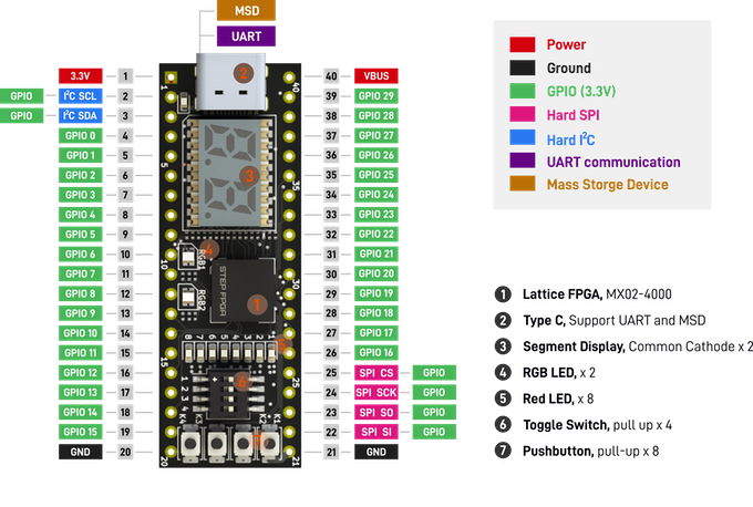
The miniature FPGA development board, the STEPFPGA MXO2Core is based on the Lattice MXO2-4000 FPGA chip. This chip is multi-purposeful and multi-functional as it incorporates features of both FPGAs and CPLDs (complex programmable logic devices). The chip’s built-in flash memory enables quick hardware configuration, which takes less than 10ms, while still incorporating 4000+ LUTs for moderate to commercial digital system design.
The board has 36 GPIO pins and by employing an internal phase-locked loop (PLL), the STEPFPGA MXO2Core’s clock frequency can be boosted from 12MHz to 400MHz. The MXO2Core board does not require the installation of any driver and takes only a few seconds to flash the chip. Additionally, the board also features a UART TX and RX module which aid in debugging with a serial COM port on your computer. The board also offers a block of RAM of 92 Kbit and a user flash of 64 Kbit.
The components of this delicate board are lead-free, and Kickstarter mentions that some of the “0201 footprints parts are just a bit thicker than your hair”. Made up of a four-layer PCB with immersion gold technology, the board features interactive components like LEDs, segment displays, switches, and push buttons allowing people to interact and examine outcomes in a tangible way. Furthermore, the DIP40 footprint offers you the option of expanding your projects on a breadboard or embedding the board in your projects.
The STEPFPGA MXO2Core board supports development on its Web-based IDE and Diamond IDE platforms. The user-friendly MXO2Core board facilitates the development of FPGA projects using the cloud-based IDE, Verilog which provides abundant pre-built examples and a simple interface. It is also compatible with the MacBook, Windows, and Linux operating systems.
Priced at $54.99, EIM Technology’s STEPFPGA MXO2Core board, also known as the STEP-MXO2, can be ordered from EIM’s Tindie store, with an expected delivery of the boards starting in July.
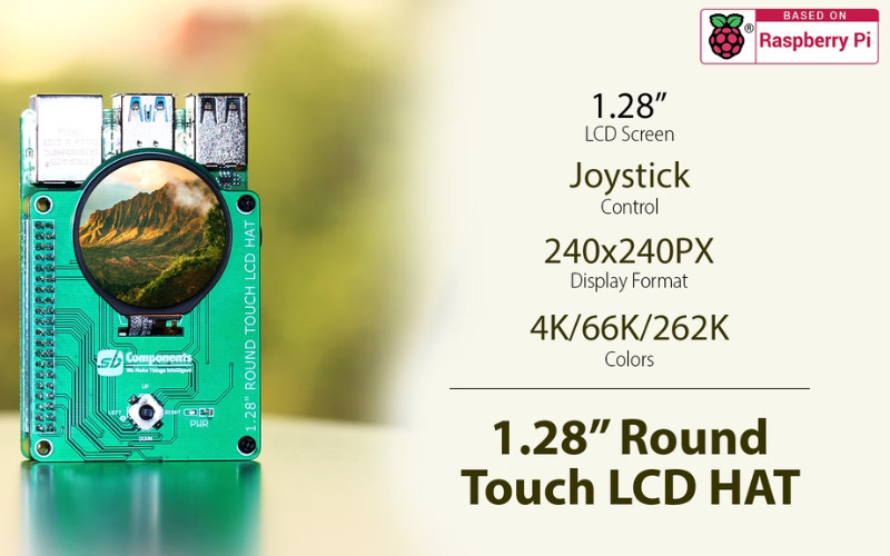
UK-based embedded device manufacturer, SB Components, has launched a crowdfunding campaign for a 1.28-inch touch LCD HAT with a goal of £3,000. The Kickstarter product page gives us more details on the 1.28-inch display, which has been over-subscribed to reach £3,522 (as of writing). This shows the community’s support to send the hardware into mass production, and the pledging options start at £38 to get the round-touch LCD HAT for your Raspberry Pi computer. The early bird £35 has been sold out, and interested people had to pledge to buy the expensive options.
At the heart of the SB Components 1.28-inch round LCD HAT is a capacitive touch control ICU with a high-performance self-capacitance touch clip. The LCD HAT has three main components as part of the hardware– a full-touch LCD display, a touch panel, and a joystick to move around for various actions. The full HD display has a resolution of 240×240 pixels and the 1.28-inch colour IPS TFT display panel has a GC9101A controller and panorama view angle. The touch panel is a capacitive screen with support for up to 13 sensing channels, and >100Hz refresh rate. The single-point gesture and two-point options are key highlights of the onboard touch panel.
Specifications of the 1.28-inch round touch LCD HAT:
Display: 1.28-inch TFT display
Resolutions: 240×240 pixels
Display connector: FPC
Color: 4K, 65K, 262K
Contrast: 500:1
Operating temperature: -22 to 70
LED lifetime: 30,000 hours
Interface: 4-wire serial SPI
Response time: 20ms
Power supply: 2.5V to 3.3V
The joystick can be seen below the display panel which is designed to provide comfort and ease while switching between different functions. It uses an SPI serial communication protocol to provide a unified platform through the standard 40-pin GPIO interface. The 5-input manual command is connected to the 1.28-inch round touch LCD HAT through a GPIO connector header. Some of the applications that can be developed using this SB Components’ 1.28 round touch LCD display HAT are weather broadcasting, security systems, home automation, multimedia applications, etc.
More details on the product are available on the crowdfunding product page. If you are interested in pledging the 1.28-inch round touch LCD display HAT, the product will be accepting pledges until July 9, 2022.
While negative feedback controls and corrects the behavior of a system, positive feedback encourages and strengthens the behavior of the system. For this reason, it is also known as regenerative feedback. Positive feedback generally occurs when the fed-back signal is in phase with the input signal and it causes the magnitude of the input signal to be increased i.e., it improves the overall gain of the system.
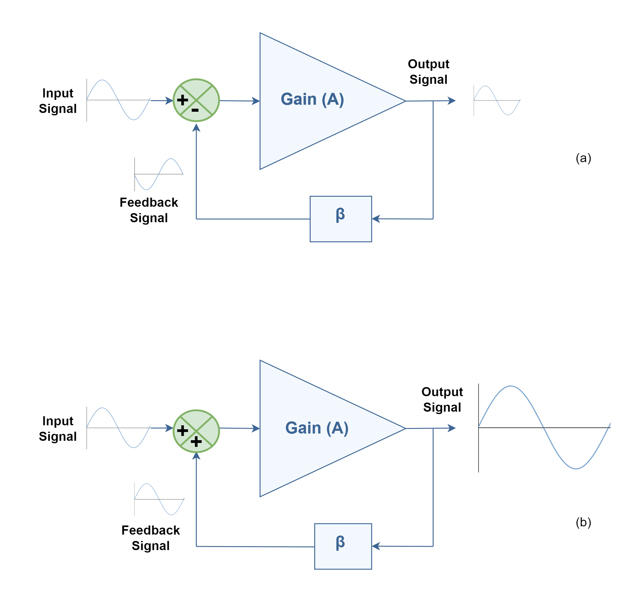
Figure 1 shows the difference between mechanisms of feeding output signal to the input terminal in the case of in-phase (positive feedback) and 180° phase-shifted (negative feedback) feeding signal. The main 2-port linear network, like an amplifier, has the open-loop gain of ‘A’ and the feedback network has the transfer function with the magnitude of ‘β’. Obviously, the feedback signal comes to the input terminal after a small delay time, and then it is combined with the input signal which is sketched here as a sinusoidal waveform.
Figure 1: Comparison of 2 types of feedback configurations containing negative feedback (a) and positive feedback (b)
A key feature of positive feedback is that small disturbances get bigger. When a change occurs in a system, positive feedback causes further change, in the same direction until the output gets as high as it can go. Under certain gain conditions, positive feedback reinforces the input signal to the point where the output of the device oscillates between its maximum and minimum possible states (upper- and lower- rails). Therefore, the amount of positive feedback allowed is typically very limited to cause only small changes to the input signal.
In practical domains, while negative feedback is often used to create controlled amplifiers and filters, positive feedback is seldom used in amplifiers, since it normally increases distortion and instability. However, the positive feedback mechanism is employed in oscillator circuits.
It should be noticed that there are also certain conditions in which positive feedback is not good for semiconductor junctions and can harm them by thermal runaway.
Positive Feedback In Op-amps
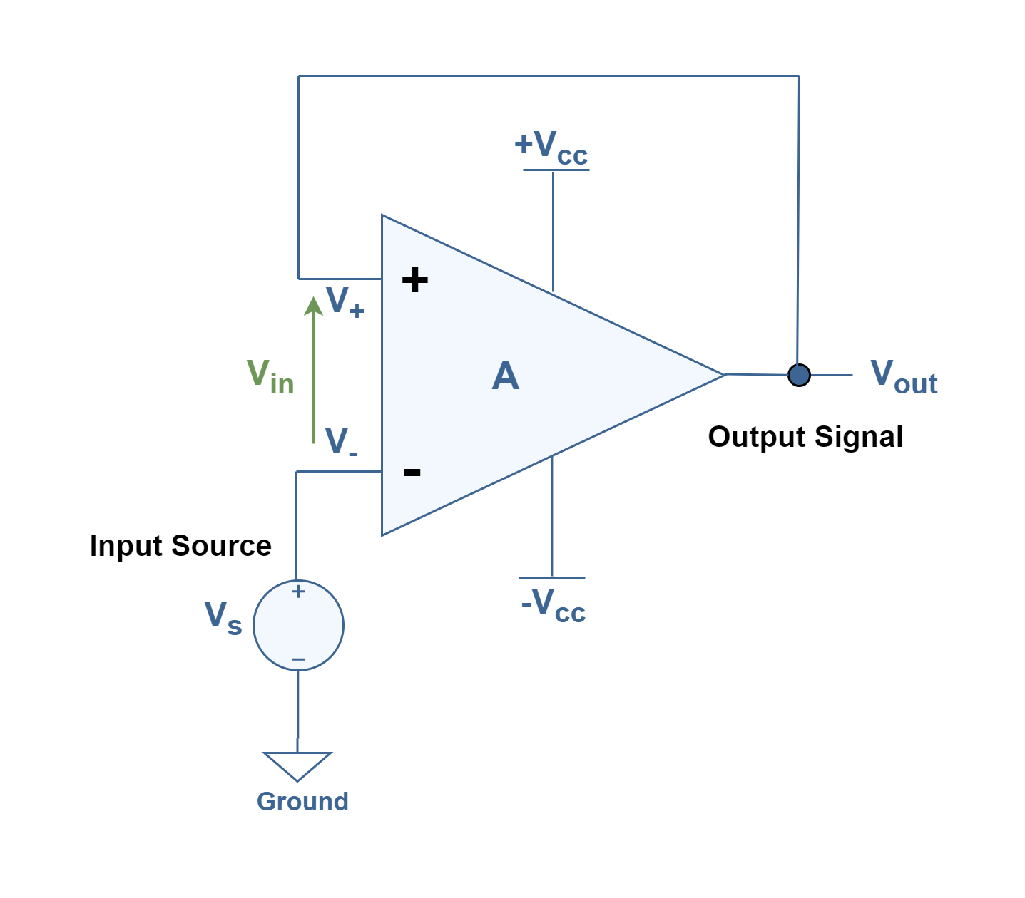
With positive feedback in Op-amp amplifiers, the feedback voltage to the noninverting input will drive the op-amp harder in the direction of the output generated signal i.e., toward saturation. Figure 2 shows the simplest schematic circuit of an op-amp positive feedback configuration by connecting directly the output terminal (Vout) to the noninverting input terminal (V+). In this arrangement, the external input voltage source (Vs) can be inserted at the inverting terminal (V–). Two positive and negative DC power supplies provide biasing of the op-amp.
Figure 2: An op-amp circuit with simple positive feedback
If the inverting input is grounded (maintaining V– terminal at zero volts by removing the input voltage source of Vs), the output voltage will be manipulated just by the magnitude and polarity of the voltage at the non-inverting input (V+). If this voltage happens to be positive, the op-amp will drive its output positive as well. Feeding that positive voltage back again to the noninverting input will result in positive output saturation which is equal to the positive power supply voltage of Vcc i.e., the upper rail. Thus:
Case 1: if V– = 0 and V+ > 0 then Vout = +Vcc
On the other hand, if the voltage on the noninverting input happens to become negative, the op-amp’s output will drive in the negative direction, feeding back to the noninverting input and resulting in full negative saturation (-Vcc or the lower rail). So:
Case 2: if V– = 0 and V+ < 0 then Vout = -Vcc
This simple analysis can be completed by applying input external excitation (Vs) and changing the voltage at inverting terminal (V–) and obtaining the same results. Therefore, what we have here is a circuit whose output is bistable; it means being stable in one of two states (saturated positive or saturated negative). Once it has reached one of those saturated states, it will tend to remain unchanged or latch in that state. By placing a voltage upon the inverting (V–) input with the same polarity, but with a slightly greater magnitude, the present state will be switched to the next.
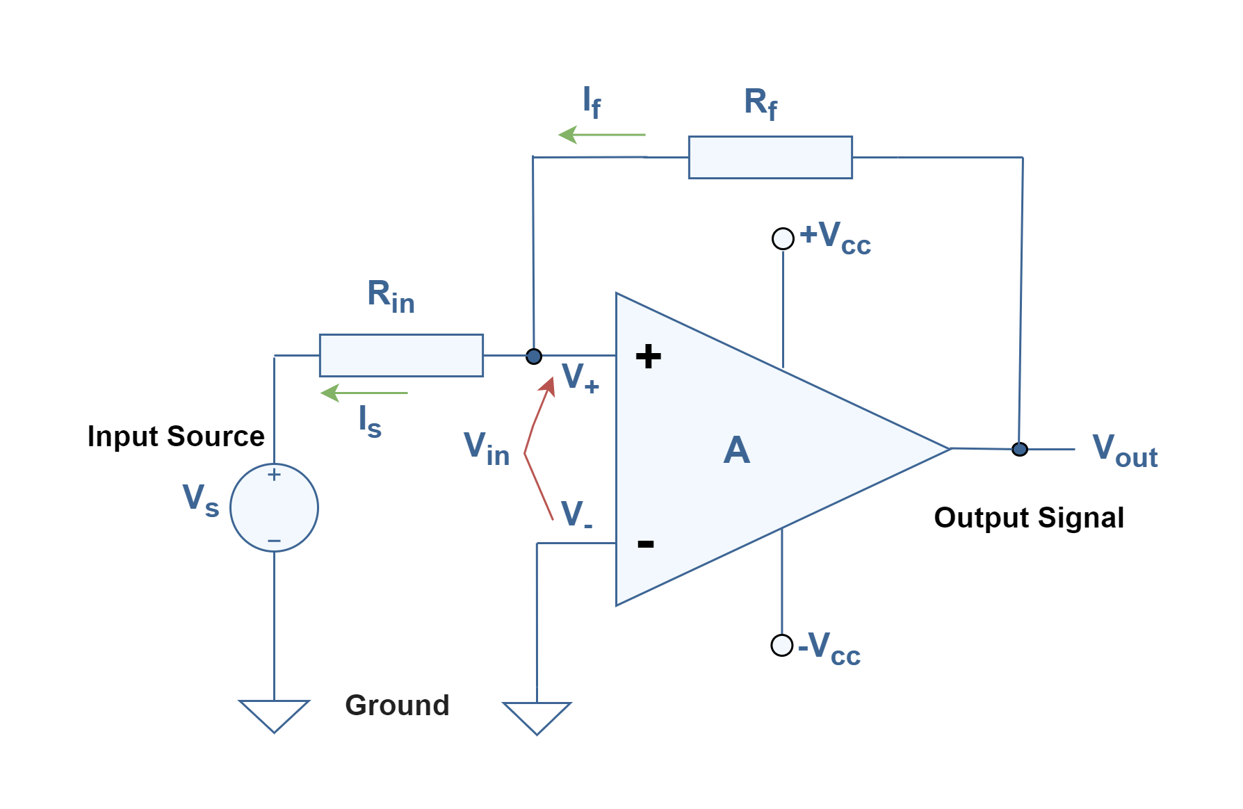
It is possible to have better control of the performance of this feedback system by adding 2 resistors between the input and the output terminals in the path of feedback. Figure 3 illustrates such a configuration by adding Rf and Rin to the op-amp and inserting an input voltage source (Vs) at the noninverting terminal (V+) while the inverting terminal (V–) is grounded.
Figure 3: Configuration of a positive feedback op-amp circuit as a comparator
One application of this circuit is a digital comparator, to convert a continuous analog signal to a two-state discrete signal. Also, by adjusting the size of the feedback resistor, a comparator can be made to experience what is called hysteresis. In effect, hysteresis gives the comparator two thresholds. By obtaining these thresholds, the comparator circuit becomes more immune to noise voltages that can produce unwanted swings in the output. The hysteresis causes the output to remain in its current state unless the input voltage undergoes a major change in magnitude.
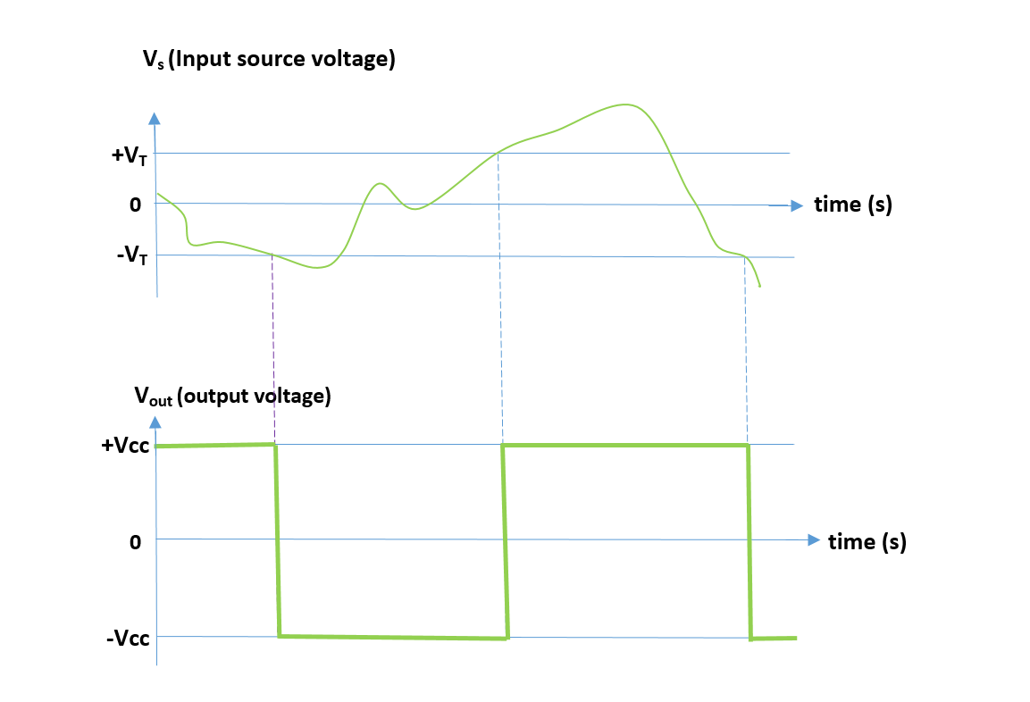
Figure 4 displays the amplitudewaveforms of the input signal (Vin) and the output signal (Vout) versus time. Vin is defined as the difference between noninverting and inverting voltages while:
Vin = V+ – V–
Figure 4: Waveforms of the input signal (Vs) and the output signal (Vout) versus time
To analyze the operation of the system we can first assume that the op-amp’s output is at positive saturation (+Vcc). Since V– is grounded, it is equal to 0 V. Because of the high impedance input characteristic of the op-amp, there is not any current inside the op-amp and the main current goes just through resistors of Rf and Rin. So, the two currents are equal; If = Is.
Using Ohm’s law:
If = (Vout – Vs) / (Rf + Rin)
By using the superposition principle, we first assume that Vs = 0, i.e., Rin is grounded. So:
Vin = Rin . If
The output remains at positive saturation (+Vcc). Now we assume that Vs has a non-zero value. If Vs is gradually reduced, there will be a point when Vin goes to 0 V, and the state of the output will be switched to another state (-Vcc). This voltage is called the negative threshold voltage (Vs = -VT) at the input. The negative threshold voltage can be determined by using the previous equations:
If = -VT / Rin = Vout / Rf = -Vcc / Rf
and then,
VT = Vcc (Rin / Rf).
Therefore, the width of the hysteresis region can be controlled by the ratio of the input and the feedback resistors. Now, if the output is at negative saturation (-Vcc) and 0 V is applied to the input (Vs = 0), Vin becomes negative and the output remains at (-Vcc). However, if the input voltage (Vs) is non-zero and it becomes increased, there is a point where Vin goes to zero, and the output switches states. This point is called the positive threshold voltage (Vs = +VT), which is equal to +Vcc. (Rin/Rf). In most applications, Rf is much larger than Rin.
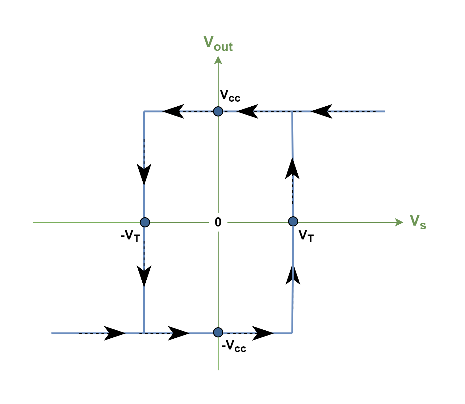
Figure 5 shows the relationship between the output saturation voltages and the margin of threshold voltages at the input. Arrows show the possible paths of changing the output voltage due to changes in the input source of voltage.
Figure 5: Hysteresis and threshold voltages in positive-feedback comparator
As Figure 4 shows clearly, applying a little positive feedback to the comparator and introducing threshold margins cause to extract of a clean square wave in the output, despite significant amounts of distortion and unwanted swings in the input signal.
The Oscillation Mechanism Of Feedback Networks
The advantages of feedback, however, are accompanied by corresponding disadvantages. Since the magnitude and phase of the gain of each network vary with frequency, it is probable in certain conditions to introduce sufficient phase-shift to cause positive feedback. Under these circumstances, the amplifier may become unstable and generate an output signal independent of the input (or without input signal); in other words, it oscillates unexpectedly.
The oscillation occurrence is mostly harmful in amplifier circuits and it is a disadvantage. But in applications like communication systems oscillators are advantageous and widely used in modulation circuits and timing applications.
For better understanding, it is important to notice the denominator in the basic negative feedback equation, Af = A/ (1 + βA). When βA= –1 or a magnitude of 1 at a phase angle of 180°, the denominator becomes 0, and the gain with feedback ‘Af’ mathematically becomes infinite or very high physically. Thus, a very small signal (like a noise voltage) can provide a measurable output voltage, and the circuit acts as an oscillator even without an input excitation.
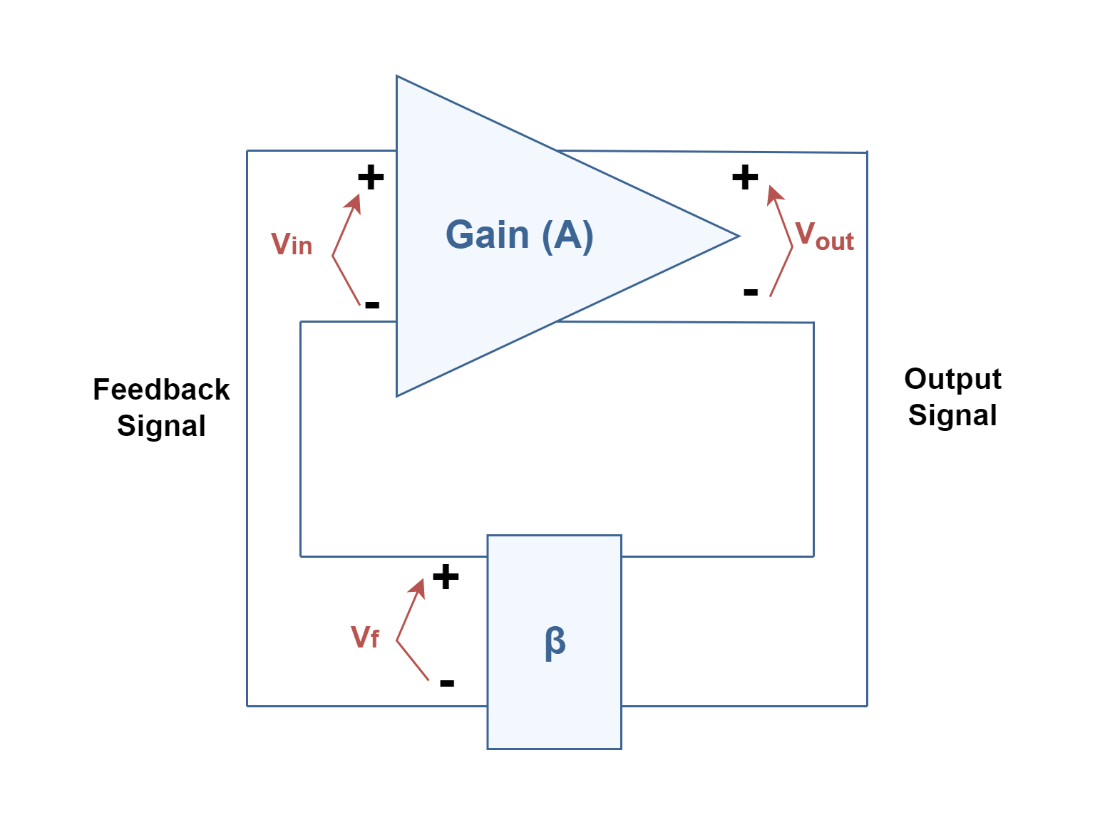
Figure 6 shows block diagrams of a general feedback system. If there is a fictitious voltage at the amplifier input ‘Vin’, it results in an output voltage of Vout = AVin after the amplifier stage and in a voltage Vf = β(AVin) after the feedback stage. Where βA is referred to as the loop gain.
Figure 6: A general feedback system without external excitation
If the circuits of the base amplifier and feedback network provide βA of a correct magnitude and phase, Vf can be produced equal to Vin. Then, when even the fictitious voltage Vin is removed, the circuit will continue operating since the feedback voltage is sufficient to drive the amplifier and feedback circuits. Therefore, the output waveform will still exist even without any input excitation, if the condition βA = 1 is met. This is known as the Barkhausen criterion for oscillation.
In practice, no input signal is needed to start the oscillator going. Only βA is made equal to or greater than 1 and the system is started oscillating by amplifying noise voltage, which is always present. Such oscillations are sometimes called parasitic oscillations.
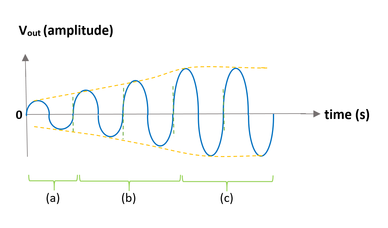
Figure 7 shows how the noise signal results in a buildup of a steady-state oscillation condition. In this waveform, three-section can be recognized: (a) In this period of time certain conditions are provided for an initial noise voltage to be amplified and appear at the output. (b) In the next period of time, this small non-sinusoidal signal (because βA is not perfectly 1) will be progressively gained in magnitude due to the positive feedback procedure. (c) the output waveform reaches a steady-state oscillation with a limited envelope due to circuit saturation conditions.
Figure 7: Generation of the periodic waveform due to oscillation in the circuit
Although positive feedback is useful in constructing oscillator circuits, unwanted oscillations render an amplifier useless. Furthermore, electronic circuits often contain unwanted but unavoidable feedback paths. The signals fed back through such paths can deteriorate performance. Similar effects caused by the stray or parasitic capacitance between the parts of an electronic component or circuit are sometimes observed.
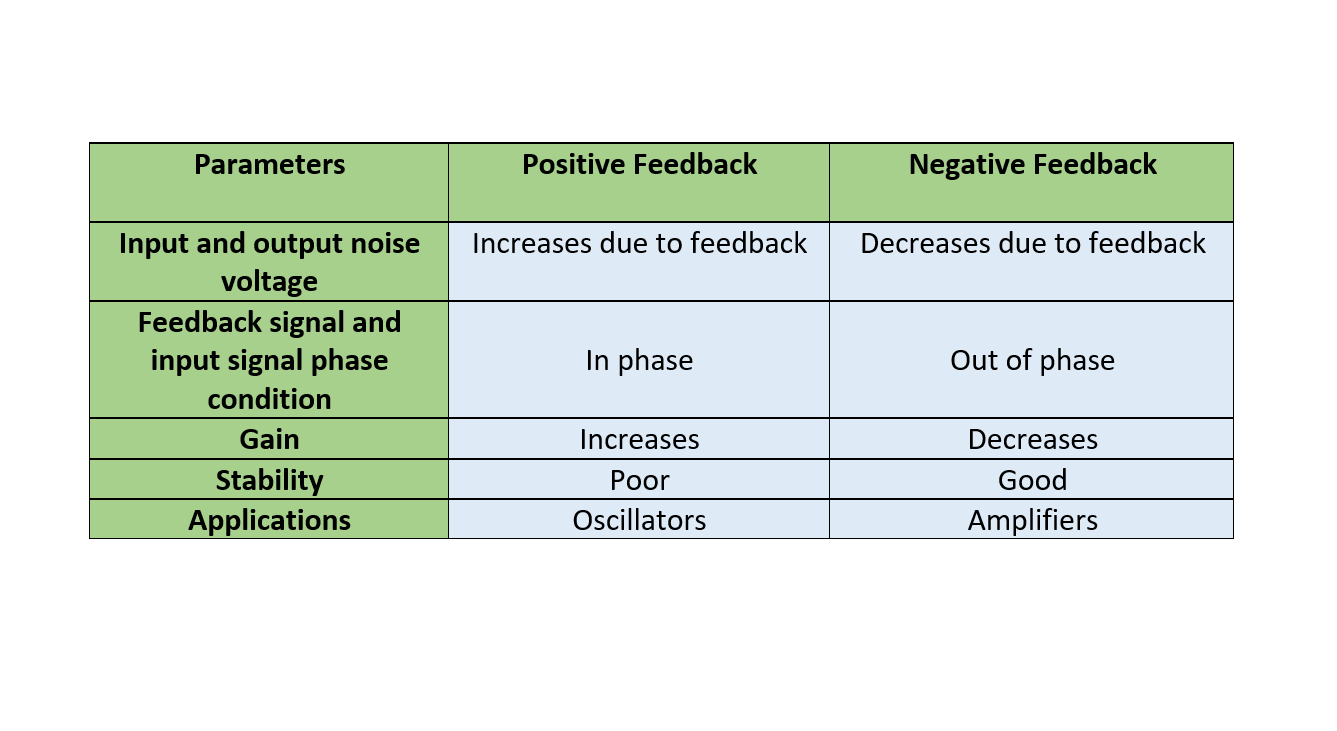
Finally, the features of negative and positive feedback systems are compared in Table 1.
Table 1: Comparison of positive and negative feedback systems
Summary
In electronics, there is the in-phase relationship between input and output in positive feedback, and the output is fed back to the positive input. This has the effect of increasing the output and going to extremes.
An op-amp with positive feedback tends to stay in the previous state of its output.
The hysteresis is an effect very commonly created using a positive feedback loop with an op-amp.
The use of positive feedback that may result in a feedback amplifier having loop-gain βA equal to or greater than 1 and satisfying the phase conditions will result in its operation as an oscillator circuit. An oscillator circuit then provides a periodic varying output signal.
Oscillators can be imagined as amplifiers with positive feedback.