Hexadecimal Numbers
The Hexadecimal (16) number is a base-16 numbering system that uses sixteen (16) numbers to represent its digit’s value. The hexadecimal number uses a group or set of four (4) binary digits to form a hexadecimal digit. In other words, a hexadecimal digit is equivalent to a nibble and we know, from the previous article, that a nibble is a four-bit binary number. The right-most nibble forms the least significant hexadecimal digit and nibbles can be added to the left of it to represent a larger hexadecimal number.
The architecture of digital systems is designed for 8, 16, 32, and 64-bit, etc. binary numbers and the presentation of these numbers in zeros (0) and ones (1) become quite confusing and complex. The reading and writing of larger binary numbers could lead to errors and information may become doubtful, indeed. The representation of larger binary numbers can be managed by using a higher base value numbering system which will accommodate more value in single-digit compared to the binary digit (bit). The octal (base-8) digit can use eight (8) numbers (0 to 7) and can accommodate a 3-bit binary number. The 3-bit binary number is quite small and not suitable for 8, 16, 32, and 64-bit architectures, etc. Likewise, the decimal number is suitable to represent a 3-bit binary number but wastes two (8 & 9) number values. In other words, an octal numbering system is more suitable compared to decimal (denary) numbers when it comes to representing binary numbers.
A suitable and appropriate numbering system is one that could accommodate a 4-bit binary number. As we know, a 4-bit number can hold sixteen (16) values (two raised to the power of four). This requires a numbering system having a set of sixteen values i.e. from 0 to 15. A digit of decimal has a range of numbers from 0 to 9 and above numbers such as 10, 11, 12, 14, and 15 cannot be represented as it involves the usage of previously used numbers. In hexadecimal, the values above nine (9) are represented by English alphabets such as A, B, and C, etc. Usage of these alphabets overcomes the problem of number repetition for ten (10) and above values.
This means A, B, C, D, E, and F in hexadecimal represent decimal numbers of ten (10), eleven (11), twelve (12), thirteen (13), fourteen (14), and fifteen (15). The same holds to represent equivalent binary numbers of “1010”, “1011”, “1100”, “1101”, “1110.” and “1111”, respectively. The difficulty of representing a larger binary number can be eased by splitting the binary number into groups of 4-bits. For example, consider (11011001110010102) which is a 16-bit binary number and the same can be written as (1101 1001 1100 10102). The latter is achieved by splitting into a group or set of 4-bits and the resultant binary number is much easier to read.
The length and complexity of binary numbers can further be reduced by converting them to equivalent hexadecimal numbers. However, hexadecimal numbers are complex compared to decimal numbers and are used only in digital systems. The 4-bit binary numbers “0000”, “0001”, “0010”, …, and “1111” are represented by a single hexadecimal digit. The 4-bit binary number is called a “nibble” which is equivalent to a hexadecimal digit. The byte is made up of 8-bits or two nibbles and as two hexadecimal digits represent such its equivalent. For example, the binary number (101001112) is split into two halves/ nibbles (1010 01112). Wherein, (10102) is equivalent to (1010) in decimal and to (A16) in hexadecimal. Similarly, the second nibble (01112), is equivalent to (7) in decimal and hexadecimal. So, altogether, the binary number (101001112) is equivalent to (A716) in hexadecimal.
Hexadecimal Numbers
The following table lists the decimal numbers from 0 to 15 against their equivalents in binary and hexadecimal numbers.
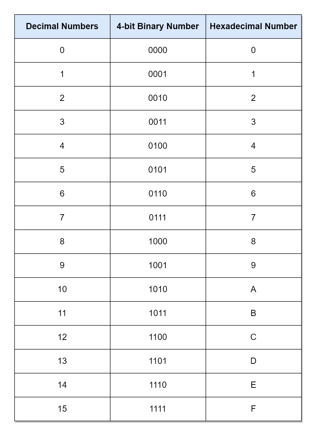
The table above shows the equivalent decimal numbers from 0 to 15 for hexadecimal digits. For counting the numbers beyond fifteen (F) in hexadecimal, the procedure similar to other numbering systems is adopted i.e. including a significant digit to the left. For example, the “16” converted to binary is (0001 0000)2 and its equivalent hexadecimal is (1016). Similarly, the 17’s equivalent in hexadecimal is the (1116), and following the same procedure, the hexadecimal number can be extended to the desired value. Using the above table, any binary number can be easily converted to its equivalent hexadecimal number. For example, a 16-bit number (1010 1100 0111 10112) converted to hexadecimal is (AC7B16). It is much easier to write and remember this hexadecimal number than a 16-bit long row of 0’s and 1’s. Hence, it is a good practice to write binary numbers in a hexadecimal numbering system in order to avoid errors, etc.
In digital systems, especially when writing programs, a “#” (hash) sign is used after the most significant digit to denote the hexadecimal value. For example, the above hexadecimal number (AC7B16) can also be written as (#AC7B).
Counting in Hexadecimal
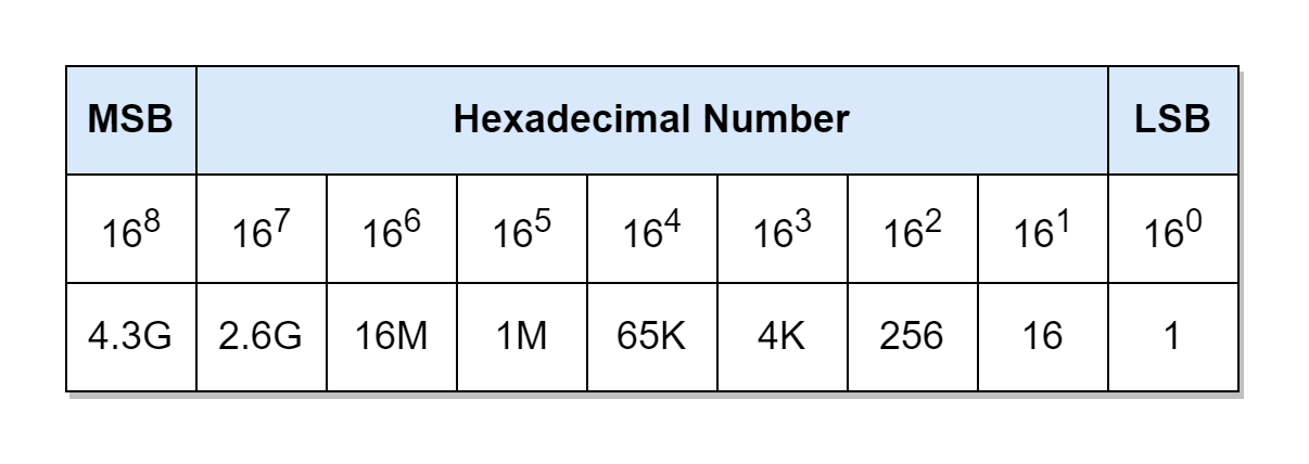
As described above, the value of a hexadecimal number can be extended by using additional significant digits. A single hexadecimal digit, starting from “0”, can count up to #F (15 X 160 = 1510) which extended to two digits can count up to #FF (15 X 161+15 X 160 = 25510). Similarly, #FFF and #FFFF can count up to 409510 and 6553510, respectively. The following table lists the weight of each digit in a hexadecimal number.
Addition of 0’s to a Binary Number
As the binary number is split into groups comprising of 4-bits in order to determine its equivalent hexadecimal number. This requires a binary number consisting of bits that are multiples of four (4) e.g. 4, 18, 12, 16, and 20, etc. However, this may not be the case when dealing with binary numbers and binary numbers can vary in bit lengths. The solution is to start splitting binary numbers, in groups of 4-bits, from the least significant bit (LSB), and, eventually, we will be left with less than 4-bits at the end. The leading zeros are added to leftover bits extending their length up to 4-bits. This group of 4-bits constitutes the most significant digit (MSD) of hexadecimal numbers. In the following table, a non-standard 13-bit binary number (1 0101 1101 101010) is converted to a 16-bit (divisible by 4) binary number by adding leading zeros, and then its equivalent hexadecimal number is determined.
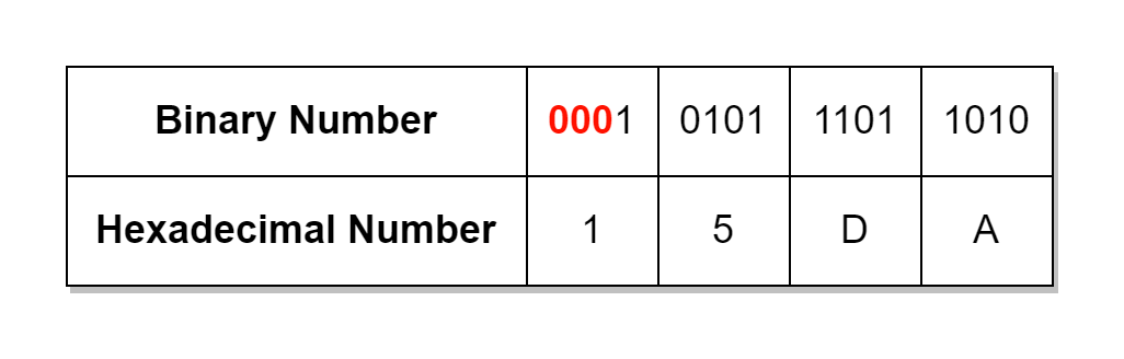
In the above example, a 13-bit number requires 3-bits having zero values to be added to the left-most side in order to make it a 16-bit binary number. Similarly, a 10-bit binary number would require six (6) zero bits to be added. The usage of hexadecimal numbers reduces the length of binary numbers by four (4) times and conversion from binary to hexadecimal or from hexadecimal to binary is easy and quick.
Hexadecimal to Decimal Conversion
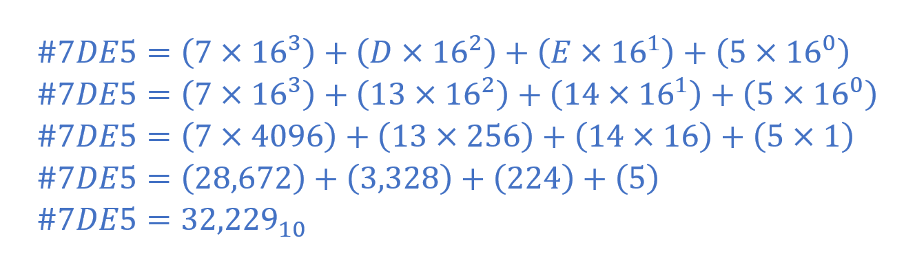
The conversion of hexadecimal to decimal value is achieved by using the weighted sum of digits method described in the previous article. In the following example, a hexadecimal number (#7DE5) is converted to a decimal number.
Decimal to Hexadecimal Conversion
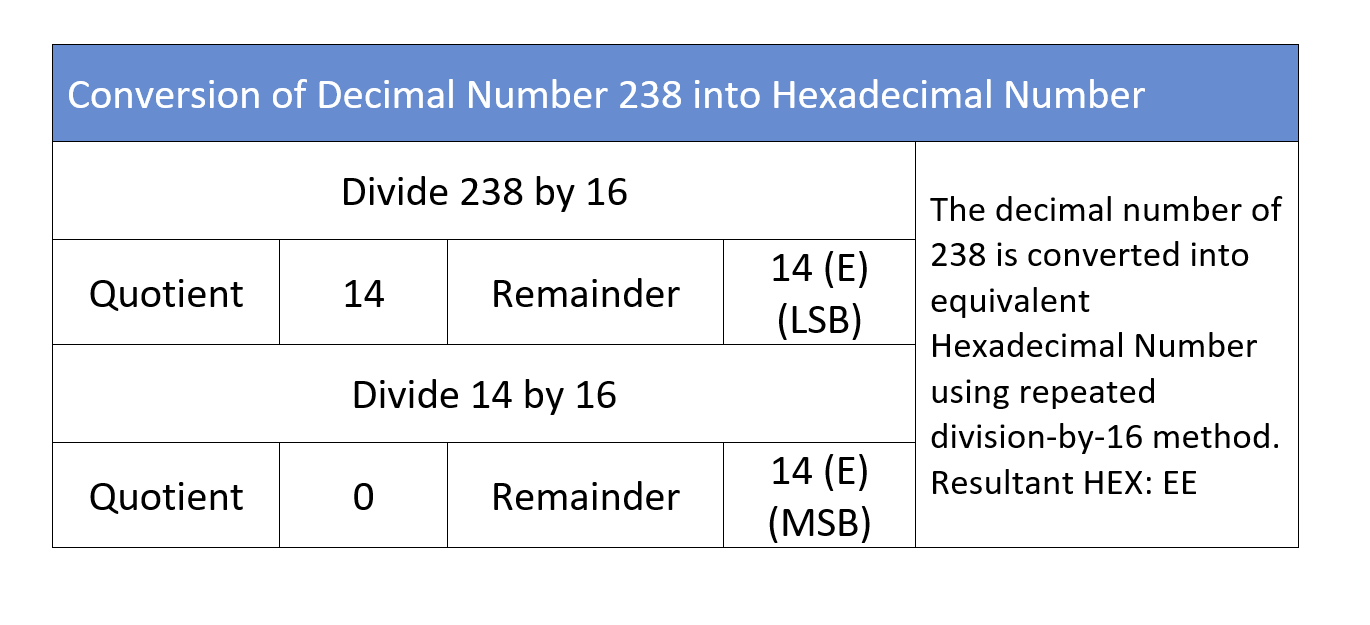
The conversion from decimal to hexadecimal requires the application of the repeated-division-by-16 method which was used to convert a decimal number to its equivalent binary value in the previous article. The same decimal number (23810) is used to obtain its equivalent hexadecimal number in the following example.
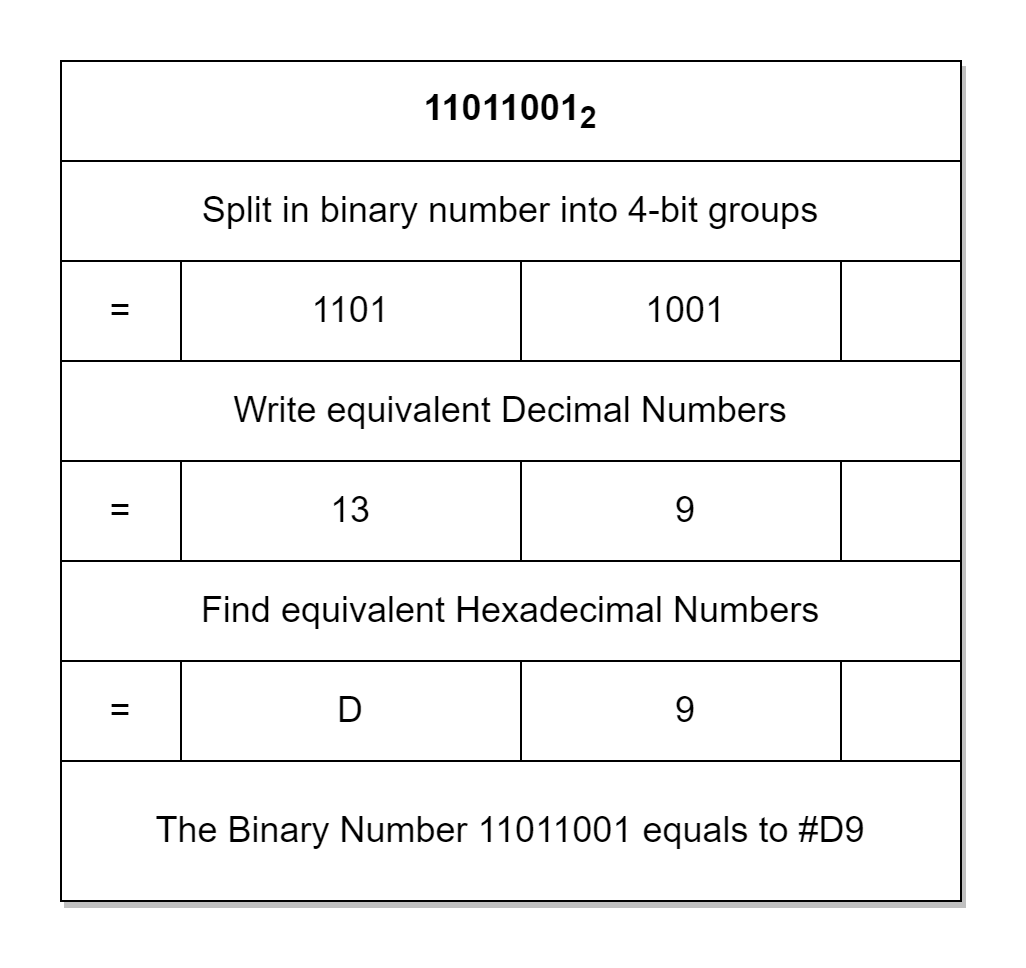
Binary to Hexadecimal Conversion Example
The conversion of an 8-bit binary number (110110012) to a hexadecimal number is shown below.
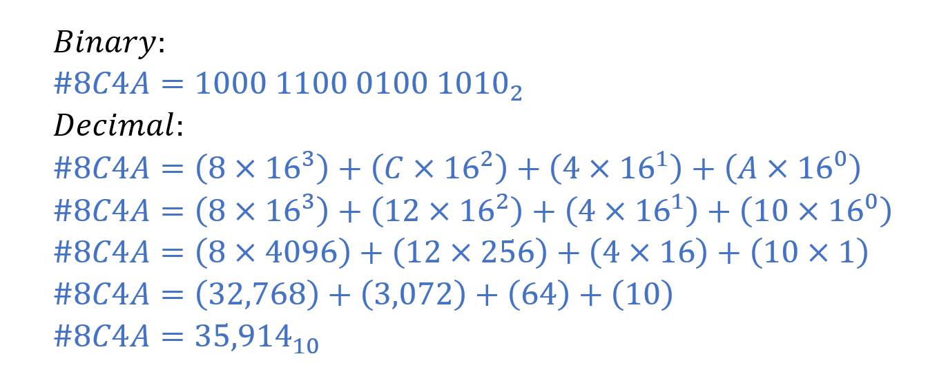
Hexadecimal to Binary and Decimal Example
The conversion of #8C4A to its equivalent binary and decimal number is shown below as an example.
Conclusion
- The Hexadecimal number uses a base-16 numbering system and its digits can have sixteen (16) numbers from 0 to 15. In hexadecimal, the capitalized alphabets: A, B, C, D, E, and F are used as equivalent to 10, 11, 12, 13, 14, and 15, respectively.
- In Hexadecimal numbers, each digit is a group or set of 4 bits. The equivalent of a binary number in hexadecimal is obtained by splitting the binary number into groups having 4 bits and then, depending on each 4-bit group’s value, an equivalent Hexadecimal value from “0” to “F” is assigned to each group.
- The binary numbers may require the addition of leading zeros on the left most (most significant) side in order to form 4-bit groups.
- The Hexadecimal number is represented by using “16” as a subscript or a hash (#) at the left-most side e.g. 2A7E16 or #2A7E.
- The Hexadecimal number can be converted to a decimal number by using the weighted sum of digits method. The conversion from decimal to hexadecimal requires the application of the repeated-division-by-16 method.
- The Hexadecimal numbers are useful in representing larger binary numbers. The Hexadecimal number reduces the length of its equivalent binary number by a factor of four (4). Moreover, the conversion from binary to hexadecimal and from hexadecimal to binary is easy and quick.