Binary to Decimal Conversion
The binary numbers are used in digital systems and computers for computing data. Moreover, the data transfer or interface between digital systems also uses binary numbers for the transfer of information. From the previous article, it is known that a binary number is a base-2 number which means that it has only two (2) numbers to represent the value of the digit. The numbers start from 0 and end at 1 making a total of two (2) numbers for the value of a digit. The binary number may contain more than one such digit such as the binary number (1001102) has six (6) binary digits. The subscript 2 at the end of the number shows that it is a base-2 number i.e. a binary number.
However, the numbering used most commonly is Decimal which is a base-10 numbering system. Each digit in a decimal number can have any of the ten (10) values starting from 0 and ending at 9. Like a binary number, a decimal number may contain more than one digit. For example, a 3824010 number has five (5) digits and a subscript 10 shows that it is base-10 i.e. a decimal number. Likewise, the addition (+), subtraction (–), multiplication (×), and division (÷) operations on decimal numbers, these mathematical operations can be applied to other numbering systems as well.
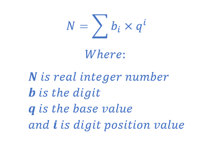
Each digit in a numbering system holds a value or weight and increases from left to right. The value or weight of each digit, from left to right, increases by base times from its preceding digit. This means that digit weight or value is given by a base value raised to the digit position. The least significant digit (LSD) has a position of zero (0). For example, a decimal number of eighty-two (8210) has two digits i.e. eight (8) and two (2). The two (2) is the least significant digit having a position of zero (0) from the right of the decimal number and, thus, its weight is 100 (1). Likewise, the second digit (the most significant digit in this case) has a position of one (1) and its weight is 101 (10). So, from right to left, the weight of each digit increases by ten (10) times for a decimal number i.e. 1, 10, 100, 1000, etc. Likewise, for a binary number, the weight increases by two (2) times i.e. 1, 2, 4, 8, 16, 32, etc.
Mathematically, a number is a weighted sum and is given by:
The Decimal Numbering System
As described earlier, the value of each digit increases by ten (10) times, left from the decimal point, in decimal numbers i.e. 100, 101, 102, 103, 104 etc. Similarly, the value of each digit decreases by ten (10) times as we move to the right from the decimal point to account for fraction numbers e.g. 10-1, 10-2, 10-3, 10-4, etc. This is because the decimal number has base-10 (modulo-10) with the position of each digit indicating the weight or magnitude of that digit i.e. q = 10. This means fifty (50), for example, can be written as 5 X 101 and five hundred (500) as 5 X10². As described above, the decimal number is equal to the sum of its digits multiplied by their respective weights. In the following text, a decimal number (N = 4125) is shown in decimal format with each digit and its weight.
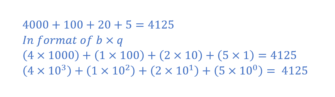
In the decimal number or any other number system, the right-most digit is the least significant digit (LSD) and the left-most digit is the most significant digit (MSD). Following this, for the above example, the five (5) is the least significant digit (LSD) which has the lowest weight i.e. one (1). Whilst, the four (4) is the most significant digit (MSD) having the highest weight of one thousand (1000).
The Binary Numbering System
As discussed earlier in this article, the binary numbering system is the fundamental numbering system in digital and computer systems. Like the decimal system, the binary numbering system follows the same set of rules except a binary number is base-2 numbering system instead of base-10. This means that the weight of binary digits varies by the power of two (2) instead of the power of ten (10). The weights of decimal digits are 100, 101, 102, 103, 104, etc. from the decimal point to the right. However, the weights of binary digits are 100, 21, 22, 23, 24, etc.
Moreover, the binary digit can hold either 0 or 1 i.e. two (bi) values. The binary number may consist of more than one binary digit and the weight or value of each binary digit increases by two (2) times from its preceding right binary digit. Therefore, following the decimal numbering system, the right-most binary digit (bit) that holds the lowest weight is called the least significant bit (LSB). Likewise, the left-most binary digit (bit) holds the highest weight and is termed the most significant bit (MSB). As the bit can have either zero (0) or one (1), the weights of bits having zero (0) values are nullified and a binary numbering system can be represented by the weights of digits having one (1) value. In the following table, the weights of a binary number’s digits and their equivalent decimal values are shown.
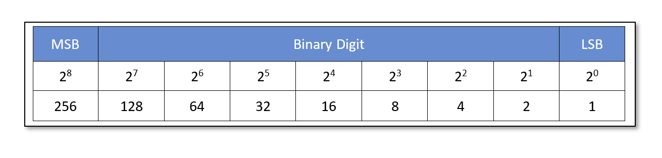
The weight of each binary digit (bit) increases (doubles) with each digit step as we move right to left. The least significant digit (LSD) has the lowest weight of one (1) and the most significant digit (MSD) has the highest weight of two-hundred and fifty-six (256).
Binary to Decimal Conversion Example
The 8-bit binary number 110100112 is converted into its equivalent decimal number. The following table lists the weight of each binary digit (bits) and their decimal equivalents.
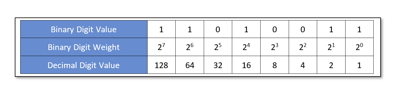
Now, using the weighted sum method, the decimal equivalent of this binary number can be obtained.
So, for a binary number, an equivalent decimal number can be easily obtained by the sum of digits weights having a value of 1. The products of zero (0) valued digits with their weights are zero and as such are accounted for in the weighted sum.
Decimal to Binary Conversion
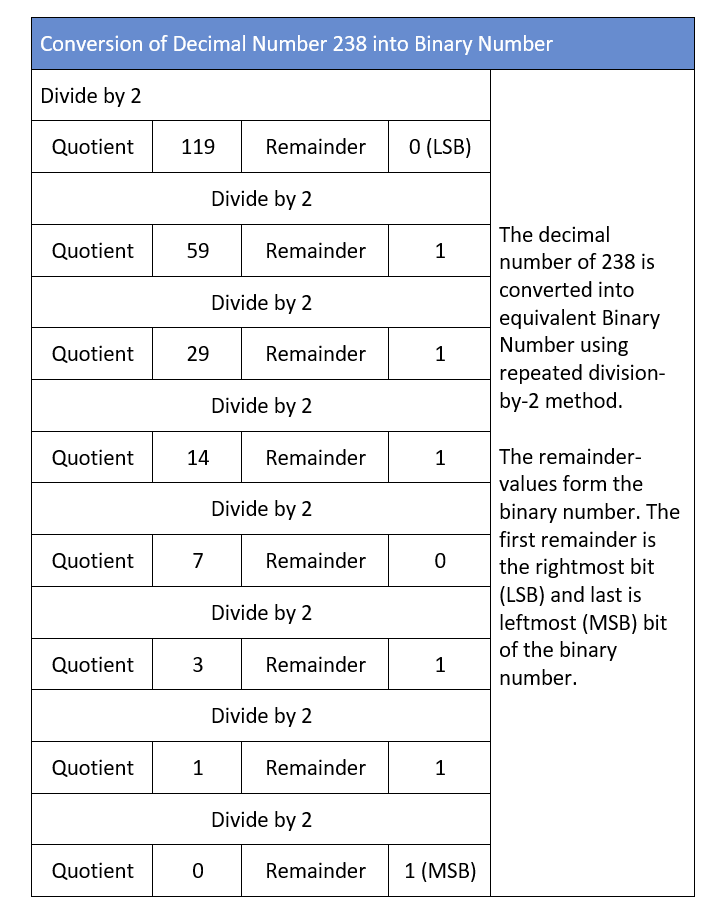
The conversion of a binary number into its equivalent decimal number is shown above using the weighted sum method. For conversion of a decimal number into an equivalent binary number can be achieved using the repeated division by two (2) method. In this method, a given decimal number is divided by two (2) resulting in a quotient and a remainder which is either 0 or 1. The quotient is repeatedly divided by 2 continuously producing a remainder until the quotient becomes zero. The remainder values achieved during the repeated division process constitute the desired binary number. The first remainder value forms the least significant bit (LSB) and the last remaining value forms the most significant bit (MSB) of the binary number.
In the following example, a decimal number of 23810 is converted into a binary number using repeated division by two (2) methods.
The same method can also be applied to convert a decimal number into another numbering system except for the division by 2 is replaced by the base value of the numbering system.
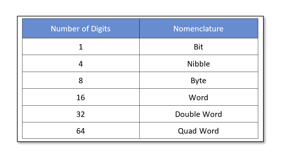
Names and Prefixes of Binary Number
Like decimal numbers, two binary numbers can also be added and subtracted together. The resulting number’s size is dependent on the sizes of binary numbers being added or subtracted. The size of the binary number is given by the number of Binary Digits (Bits) and the number of bits is classified into different sizes and names. In the following tables, the number of bits is classified into larger groups and their respective name are also given.
It is pertinent to mention here that one should be careful in interpreting the numbers as the digit values of decimal numbers (from 0 to 9) are also included in binary and octal numbering systems. For example, a number 101 could mean a binary, octal, or decimal number. Likewise, a number 234 could be an octal or decimal number. Normally, a number given without any base value or numbering system means a decimal number. It is good practice to mention the number with its base value as a subscript e.g. 1012 (binary number) or 10110 (decimal number).
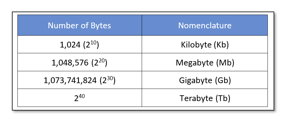
The memory size of digital systems and computers is given in bytes which groups eight (8) bits together. Like other measurement units, prefixes are added to represent larger values. The following table lists the most frequently used prefixes to represent binary numbers.
Conclusion
- A binary number is a base-2 numbering system that is composed of binary digits, called bits.
- A bit may have a value of either “0” or “1” that is its value can hold only two (bi) numbers.
- The magnitude or weight of a bit’s values doubles (power of 2) from its preceding bit (from right to left).
- The rightmost bit is termed as least significant bit (LSB) and has the lowest weight in a binary number.
- The leftmost bit is termed as most significant bit (MSB) and has the highest weight in a binary number.
- The binary number can be converted to a decimal number using the sum-of-weights method which sums the products of each digit’s value with its weight.
- The decimal number can be converted into a binary number using the repeated-division-by-2 method which divides the decimal number into quotient and remainder. The remainders constitute the desired binary number until division results in a 0 quotient. The first and last remainders form the LSB and MSB, respectively.
- It is a good practice to mention the numbering system along with the number by writing the base value as a subscript to avoid misinterpretation.

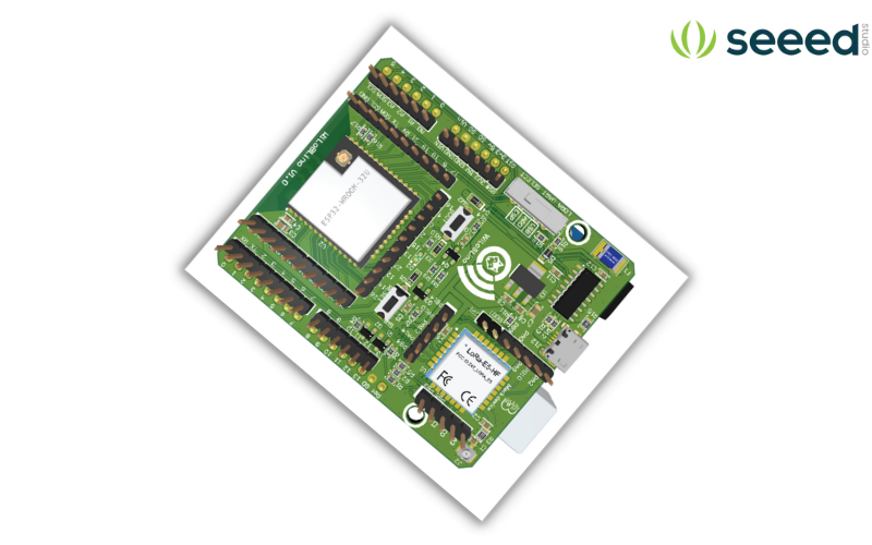
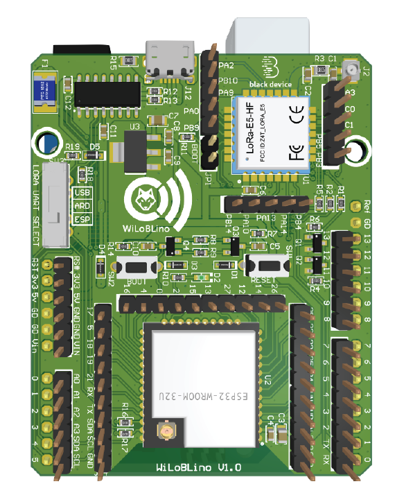
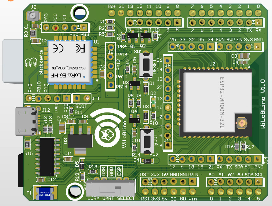
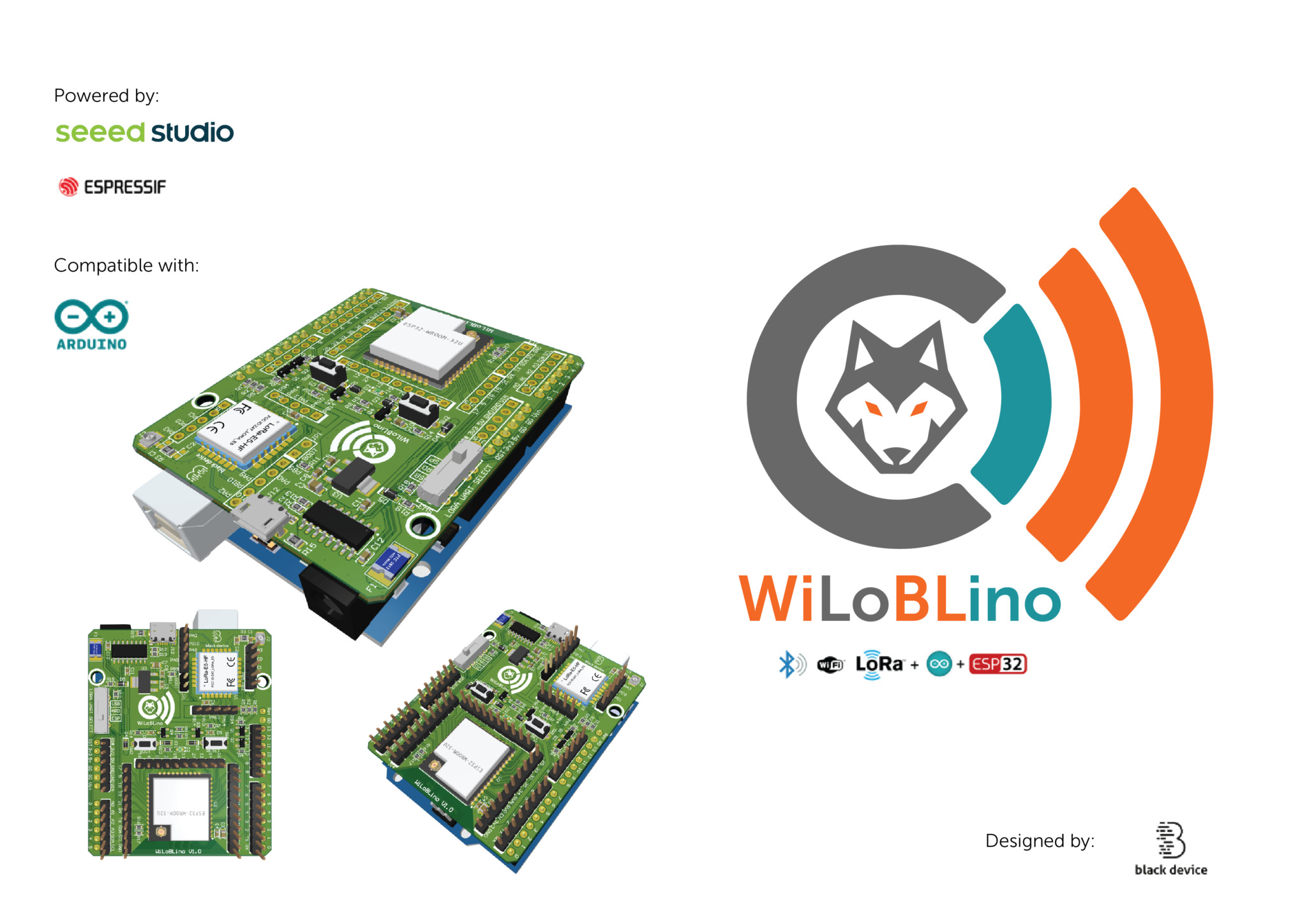 Chinese embedded device manufacturer, Seeed Studio, along with Antonio Cotos Facal, CTO of Black Device have designed a WiLoBLIno hardware platform fueled by the in-house Seeed Studio’s LoRa-E5 and ESP32 modules. WiLoBLIno name is derived from Wi-Fi (Wi), LoRa (Lo), Bluetooth (BL), and Arduino-compatible stack (Ino). The hardware is still in the development phase, but Seeed Studio’s Amanda Sun, overseas marketing and development manager decided to reveal some details and schematics of WiLoBLIno. Through a rich set of wireless communication support, WiLoBLIno is expected to make its way through the overcrowded embedded device industry. The flexibility to interface with Arduino development boards enables the user to take advantage of the existing modules and sensors.