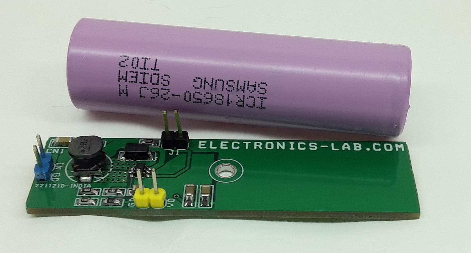
The project presented here is capable of supplying 400mA of current from a 3.7V Li-Ion/Li-Po Battery input with a 5V output. The converter has an internal soft start and internal frequency compensation features. The project is built using LTC3426 SOT23-6 chip. The LTC3426 chip is in a low profile (1mm) SOT-23 package and has a very low shutdown current of about 0.5µA. A switching frequency of 1.2MHz allows a tiny solution. The tiny PCB can be mounted on the backside of the a 18650 battery holder. Jumper J1 is the shut-down jumper. Internal soft-start eases inrush current issues.
Li-Ion/Li-Po 18650 Battery to 5V Boost Converter – [Link]
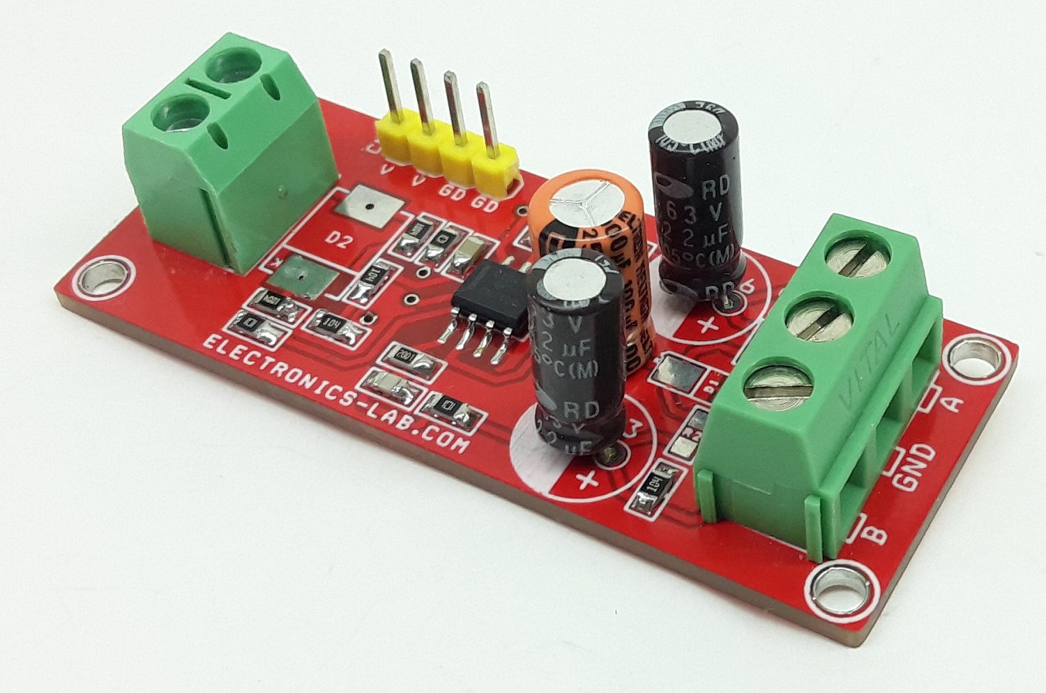
The board presented here is a preamplifier for contact microphones that are used for amplifying the sound of musical instruments which do not contain electrical pickups, such as guitar and violins. Most contact microphones use a piezo element to convert vibration in the body of the musical instrument to a voltage. The circuit is built using OPA1678 OPAMP. The low noise and low input bias current of the OPA1678 makes the device an excellent choice for high impedance preamplifiers for piezo elements. This preamplifier circuit provides high input impedance for the piezo element but has low output impedance for driving long cable runs. It provides a balanced audio output that can be fed to a balanced microphone pre-amplifier. The circuit has also the option for phantom power input. Install R3=1.2K Ohms, R2=1.2K Ohm and Zener diode 24V.
Piezo Element Amplifier for Guitar and Violin – [Link]
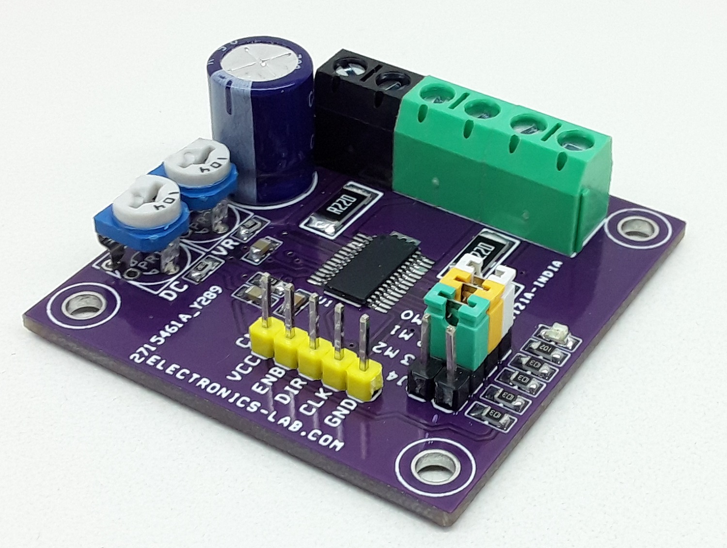
The project presented here is a bipolar stepper motor driver. It is based on BD63731EFV chip which is a low-consumption driver that is driven by a PWM signal. The power supply voltage of the project is 8 to 28V DC, and the rated output current is 3A. CLK-IN driving mode is adopted for the input interface, and excitation mode is corresponding to FULL STEP mode (2 types), HALF STEP mode (2 types), QUARTER STEP mode (2 types), 1/8 STEP mode, and 1/16 STEP mode via a built-in DAC. In terms of current decay, the SLOW DECAY/FAST DECAY ratio may be set without any limitation, and all available modes may be controlled in the most appropriate way. In addition, the power supply may be driven by one single system, which simplifies the design.
High-performance, High-reliability Bipolar Stepper Motor Driver – [Link]
The project presented here is a high common-mode current sense amplifier with two high-speed comparators to detect out-of-range current conditions. The comparators are configured to detect and respond to dual over current conditions. These devices feature an adjustable limit threshold range for each comparator set using an external limit-setting resistor. Limit 1 Resistor is R10 and Limit 2 Resistor is R11. The board measures differential voltage signals on common-mode voltages that can vary from 0 V up to +36 V, independent of the supply.
Current-Sense Amplifier with Dual Over Current Level Monitor & Alert Output – [Link]
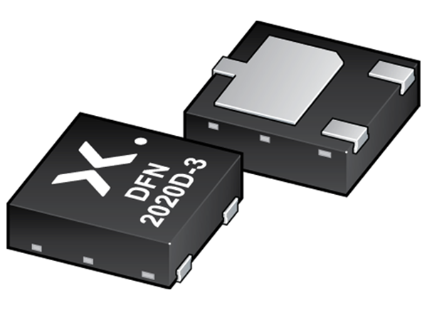
Nexperia PBSS4310PAS-Q NPN Low VCEsat Transistor features a very low collector-emitter saturation voltage, high collector current capability, and high efficiency due to less heat generation. The PBSS4310PAS-Q is housed in an ultra-thin SOT1061D (DFN2020D-3) leadless small Surface-Mounted Device (SMD) plastic package with medium power capability and side-wettable flanks (SWF). The leadless small SMD plastic package with solderable side pads reduces printed circuit board (PCB) area requirements.
Features
Very low collector-emitter saturation voltage VCEsat
High collector current capability IC and ICM
High collector current gain (hFE) at high IC
High efficiency due to less heat generation
High-temperature applications up to 175°C
Reduced Printed-Circuit Board (PCB) area requirements
Leadless small SMD plastic package with solderable side pads
Exposed heat sink for excellent thermal and electrical conductivity
Suitable for Automatic Optical Inspection (AOI) of solder joint
Qualified according to AEC-Q101 and recommended for use in automotive applications
A UPDI USB programmer (Unified Program and Debug Interface) is basically an Atmel / Microchip proprietary programming interface used for some AVR microcontrollers like the ATtiny series. AVR is an 8-bit RISC architecture microcontroller that is developed by Atmel. With the newer generations of technology, Microchip started releasing a new series of ATtiny chips called the ATtiny 1-series, followed by a lower cost range called the ATtiny 0-series. As their name suggests they are mainly used for small applications. They can make use of the new Arduino core called megaTinyCore.
These AVR microcontrollers can be programmed in two ways either using a serial peripheral interface (SPI) or UPDI. The Serial Peripheral Interface is a full-duplex master-slave-based interfacing technique. In this technique, the programming is done by the rising or falling edge of the clock applied. One disadvantage of the SPI interface technique is that the speed of synchronization depends on the target clock. Additionally, it uses four pins for the interface.
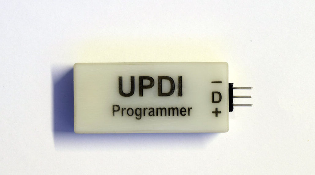
On the other hand, the UPDI method of programming is the latest interface developed by Microchip. It is used for almost all the new AVR microcontrollers like tinyAVR, megaAVR, and AVR-Dx. The UPDI UBS Programmer is based on the PDI two-wire physical interface. It combines Debug-Wire and PDI and has a single one-wire interface. It provides a bidirectional half-duplex asynchronous communication with the microcontroller device to perform the programming and debugging of the device. It is a small and compact programmer and with the help of the USB, it can be directly plugged into a computer for easy and efficient communication.
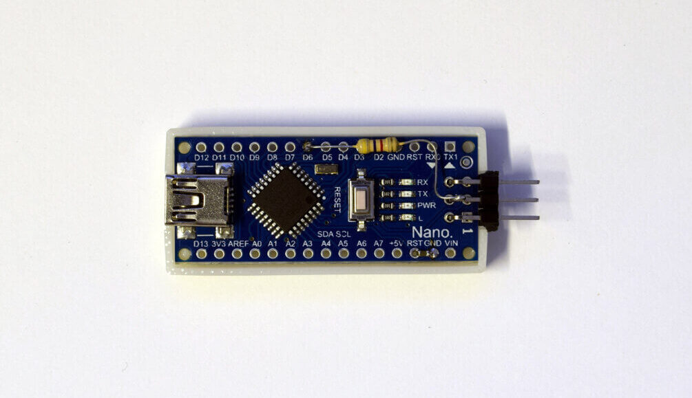
The original UPDI USB Programmer is sold at a high price hence some enthusiasts have made their own DIY UPDI programmer using cheaper hardware that is more commonly available. This DIY programmer can be made by modifying just a few hardware components and uploading the firmware on it. It uses the following components: An Arduino Nano board or any other compatible board, a resistor, a capacitor, and 6 pins angled header. These components can be directly soldered to the Arduino board making it manageable and enabling the programming of UPDI devices over a USB connection. The microcontroller board can then be used as-is or encompassed in a 3D printed enclosure to make it more robust. As for the software, a GitHub repository demonstrates how to make a UPDI USB programmer by installing the ElTangas’s jtag2updi firmware on an Arduino Uno, or any other ATmega328-based Arduino board.
Working with the UPDI USB Programmer
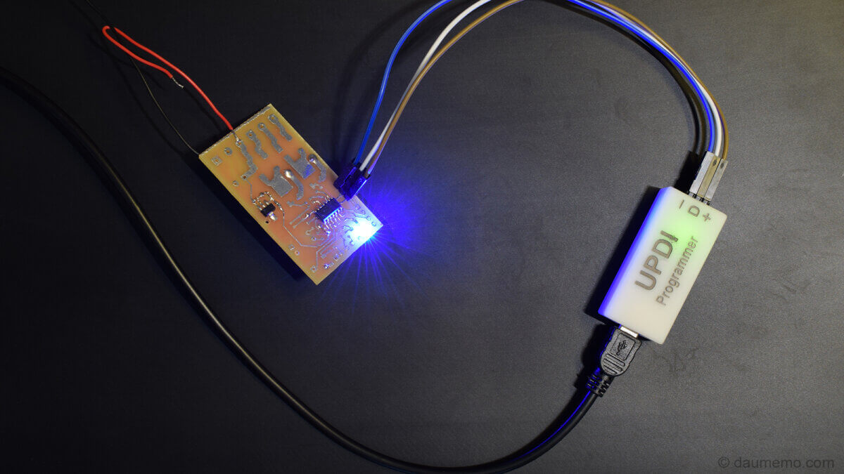
This DIY UPDI USB programmer successfully works in both Microchip Studio with AVRDUDE or PlatformIO and provides a much needed cheaper alternative that can be easily made by just following a few steps. You can watch the below youtube video for detailed steps with more information. You can also visit Daumemo’s blog for a detailed explanation.
Seeed Studio’s reComputer Jetson series has been around for a while, and are compact edge computers built around the famous NVIDIA Jetson modules for AI embedded applications. The manufacturer continues to add more devices to the list with the all-new reComputer hand-sized edge AI computer powered by the NVIDIA Jetson Nano production module, capable of delivering 128 NVIDIA CUDA cores with a performance of 0.5 TFLOPs.
As designed for edge AI applications at scale, the reComputer Jetson aims to accelerate next-gen AI product development by deploying DNN models and ML frameworks for edge inferences. Some of the tasks where the hardware is expected to perform exceptionally well are real-time classification and object detection, pose estimation, semantic segmentation, and natural language processing.
The reComputer Jetson edge computer comes in the same design as the Jetson Nano Developer’s Kit reference carrier board with a rich set of input/output ports, including a Gigabit Ethernet port, USB 3.0 and 2.0 ports, and HDMI port.
Capable of running a wide range of advanced networks, the Jetson Nano offers the complete native implementations of prominent machine learning frameworks such as TensorFlow, PyTorch, Caffe/Caffe2, Keras, and MXNet, among others. Furthermore, the reComputer Jetson series extends its compatibility with the entire NVIDIA Jetson software stack, which includes AI frameworks, development platforms like Edge Impulse and AlwaysAI, and cloud-based robot development tools such as Nimbus. With the intent to reduce time to market, Jetson Software enables this by providing end-to-end acceleration for AI applications.
Specifications of the reComputer Jetson-10-1-A0
Module: NVIDIA Jetson Nano (production version)
CPU: Quad-core ARM A57 clocked at a frequency of 1.43 GHz
GPU: 128-core NVIDIA Maxwell
Storage: 16GB eMMC
Memory: 4GB 64-bit LPDDR4
AI performance: 472 GFLOPS
USB: 1x USB 3.0 Type-A Connector, 2x USB 2.0 Type-A Connector, 1x USB Type-C for device mode
The system is a general name that indicates several meanings and concepts. The Merriam-Webster dictionary defines a system as “a regularly interacting or interdependent group of items forming a unified whole”. A physical system is a unit or a combination made up of physical objects as its elements/ components and possibly subsystems, which act together and perform a certain objective; like a computer system or a power distribution system. A subsystem can also be considered a system itself.
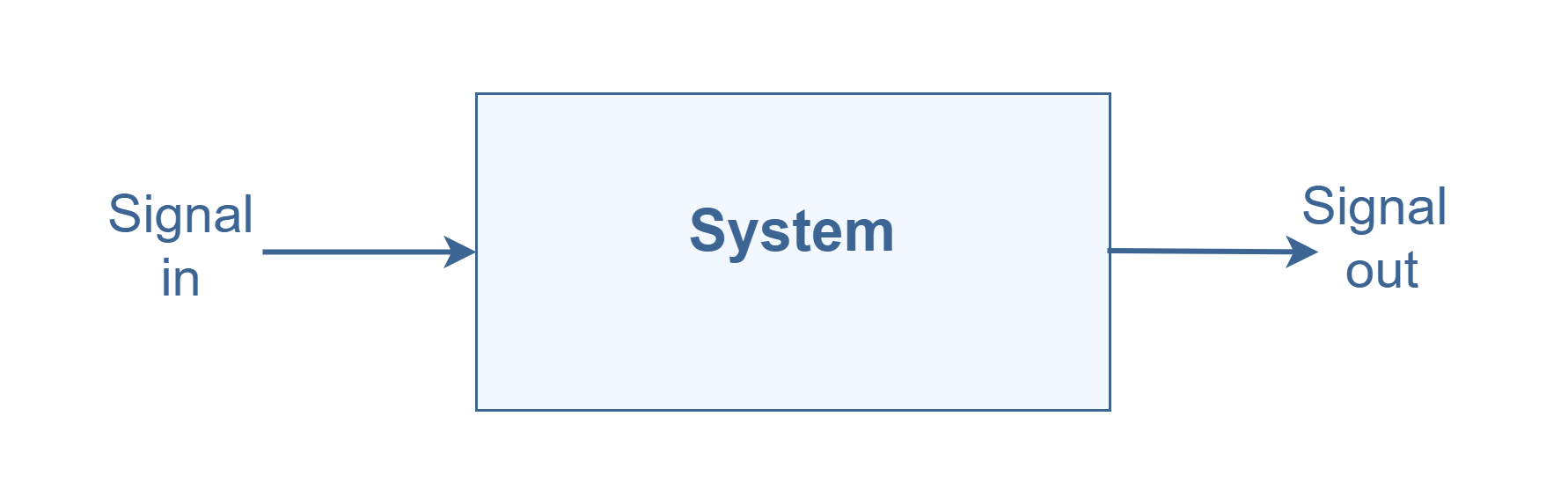
A system, like a physical device or circuit, can be represented as a black box that shows how the system produces an output signal in response to an input. A signal is also a description of how one parameter varies with another parameter; For example, voltage changing over time in an electronic circuit. A block diagram of a system is a pictorial representation of the functions performed by each component and the flow of signals. It can be obviously useful to simplify the description of sophisticated systems containing several elements. Figure 1 shows a block diagram of a simple system with input and output ports.
Figure 1: A simple block diagram of a system with 2 ports
The behavior of systems is often governed by certain physical laws or constraints; for example, Kirchhoff’s laws of voltage and current in electrical systems (KVL & KCL). In terms of system theory, the problem is to find how the system transforms the input signal into the output signal. To design or analyze the performance of a given system, the first step is to establish a mathematical model based on physical laws, usually in the form of a set of (differential) equations. The output results are then extracted from input signal values by solutions of the mathematical model.
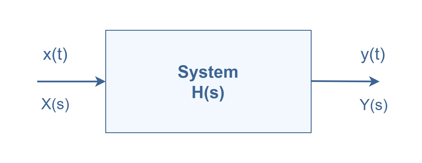
In system theory, for a linear, time-invariant (LTI) system, it is appropriate to use the transfer function (also known as system function or network function) of a system as a mathematical model (in the Laplace domain) that relates to the output response to the input variable.
The transfer function of an LTI system is defined as the ratio of the Laplace transform of the output (response function) to the Laplace transform of the input (driving function) under the assumption that all initial conditions are zero. The transfer function is the property of a system itself, independent of the magnitude and nature of the input or driving function. By applying Laplace transform we switch our analysis from a function of time to a function of the variable s (complexfrequency):
Equation 1: Definition of the transfer function
Therefore, as a more complete representation of a system block diagram, the transfer functions (usually denoted by H(s) or T(s)) of the components are entered in the building blocks (Figure 2). This representation is so powerful because they simplify understanding of systems i.e. the transfer functions reduce the differential equations to simple algebraic equations.
Figure 2: Representation of a system with transfer function H(s)
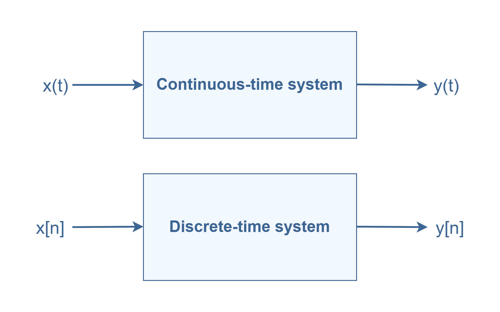
In system theory, some rules are used for naming signals. First, continuous-time signals use parentheses, such as x(t) and y(t), while discrete-time signals use brackets, as in x[n] and y[n]. Second, time-domain signals use lower case letters. Upper case letters are reserved for the frequency or Laplace domain alternatively. Figure 3 shows how we can symbolize a system.
Figure 3: Representation of continuous and discrete-time systems
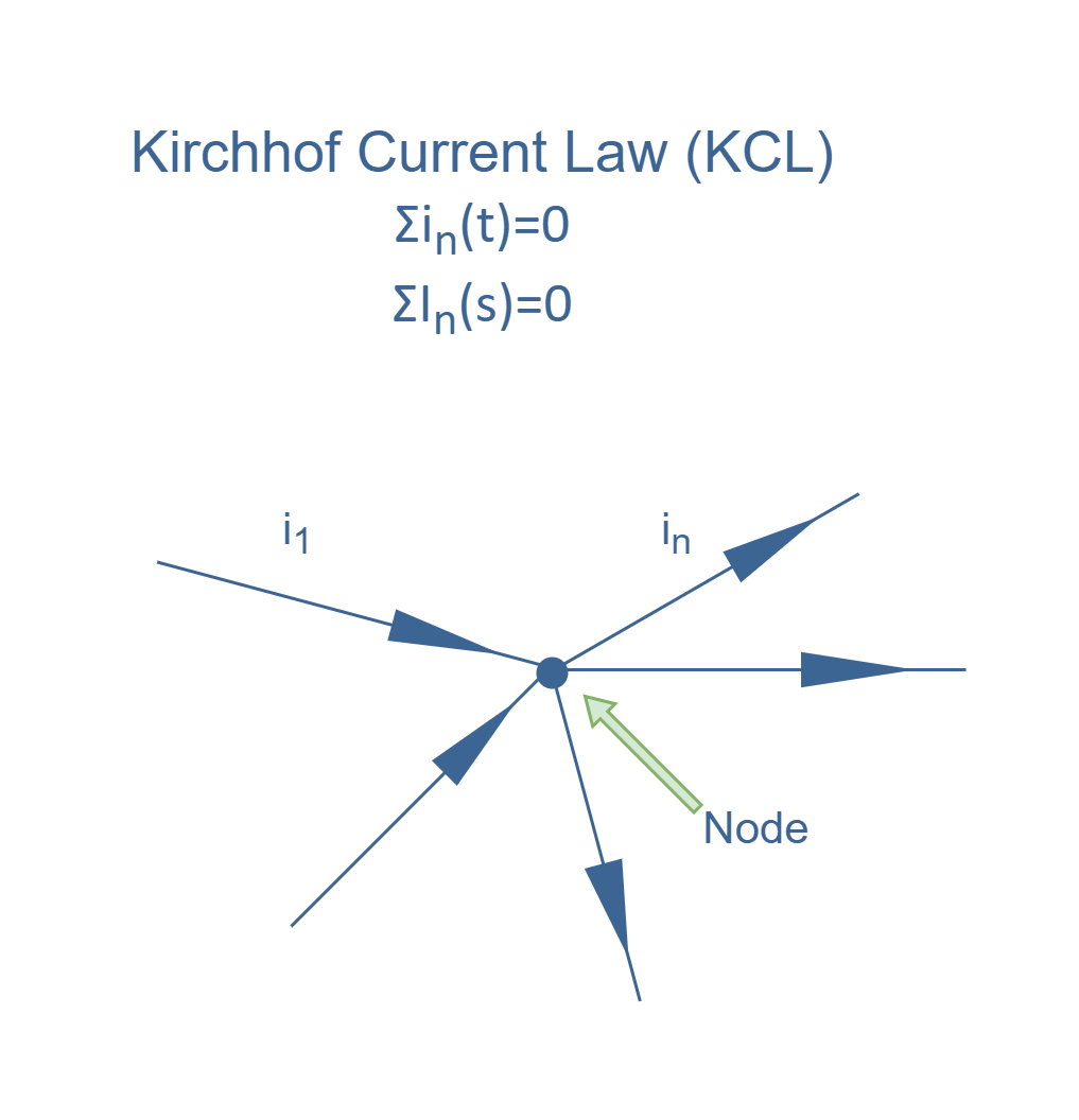
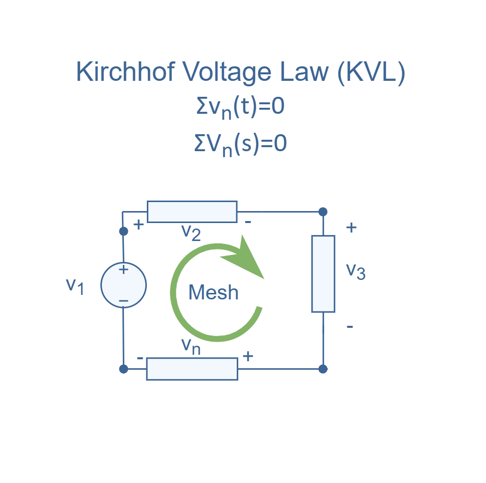
In electric circuit theory, a circuit can be composed of resistors, capacitors, inductors, voltage and/or current sources, etc. The analysis of this system is normally based on the circuit topology i.e. a schematic diagram of the circuit containing the symbols of its elements, their connections, and numerical values relating its terminal voltage and current for each of these circuit elements at every instant of time. when the voltage-current relation for each element is specified, Kirchhoff’s voltage and current laws can be applied possibly together with the physical principles (Figure 4). Then, the mathematical model can be created.
Figure 4: Kirchhoff current and voltage law in time and frequency (Laplace) domains
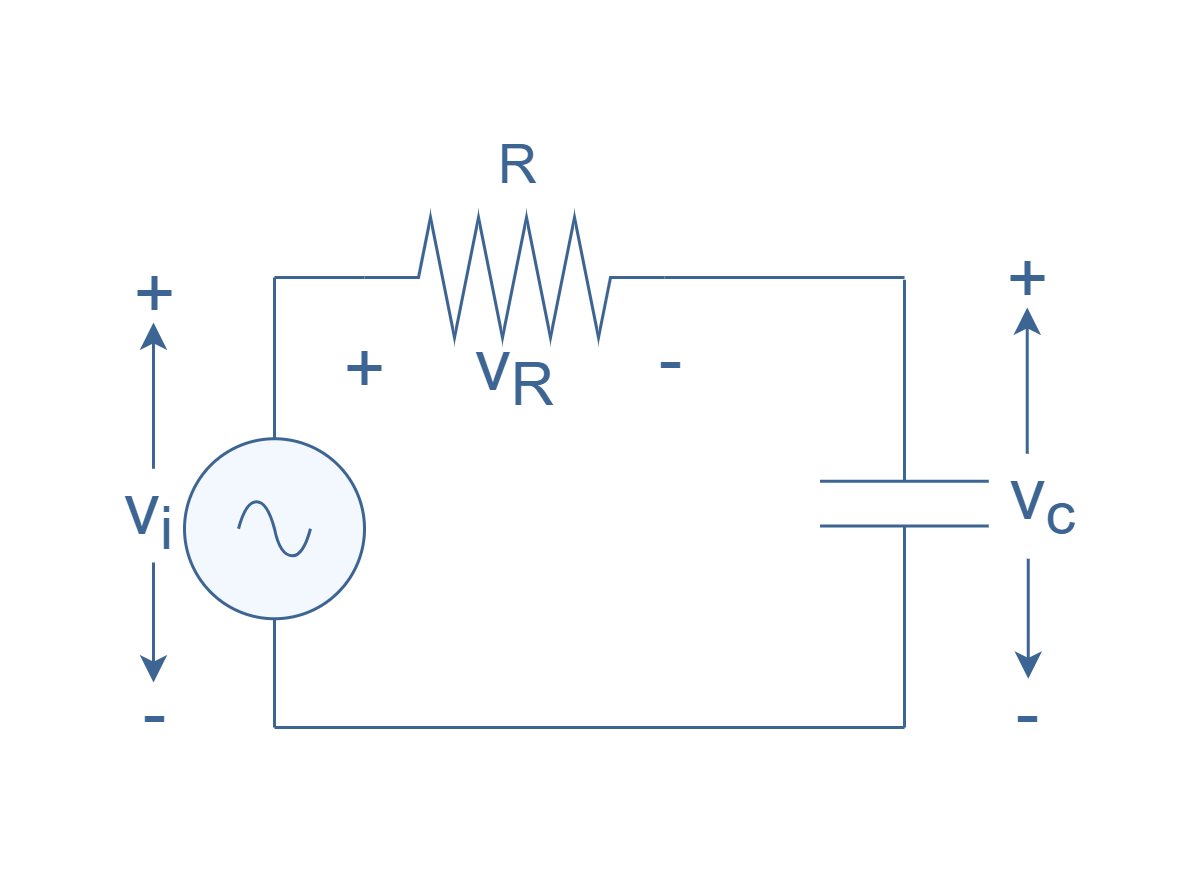
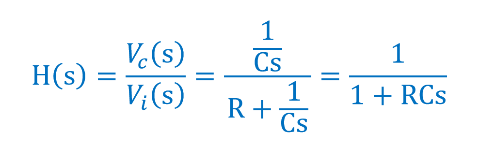
As a simple example for circuit theory analysis, Figure 5 describes a system consisting of an RC circuit using an input voltage source with the instant value of vi(t) and output of measured voltage of vc(t) across the capacitor:
Figure 5: Example of an RC circuit
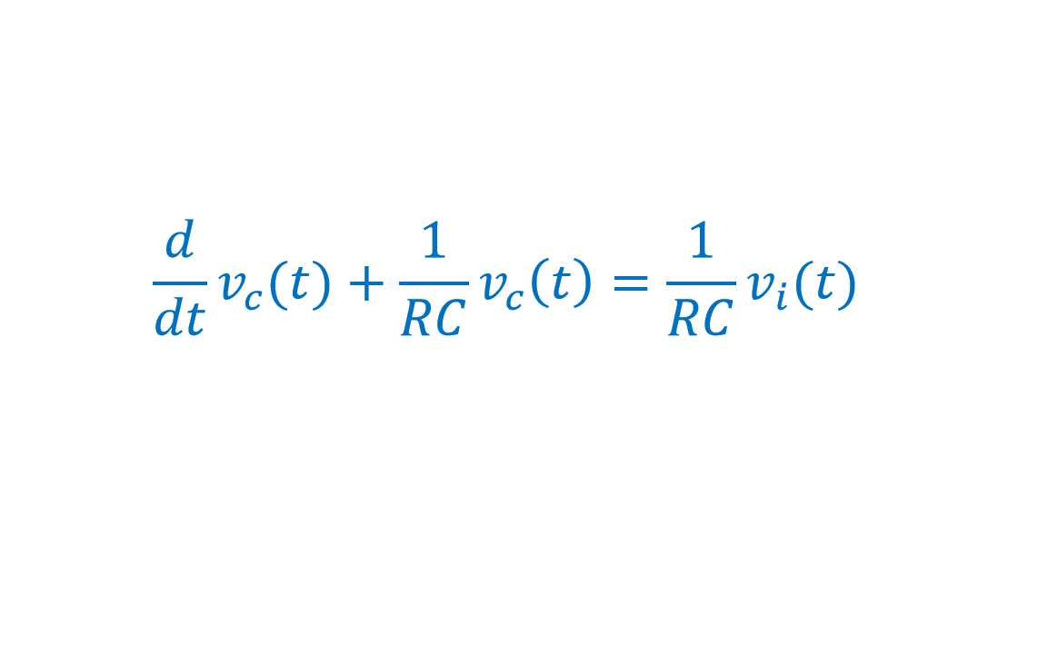
In this electric RC circuit, application of KVL and Ohm’s Law leads to the following differential equation describing the input/output behavior:
Equation 2: The differential equation as a mathematical model
Another method, as mentioned above, is to find the equation in the Laplace domain.
we can place the equalities as:
Z1 = R and Z2 = (1/Cs)
Then, we can use the voltage divider concept with the voltage across the capacitor as the output response. The transfer function is then obtained as:
Equation 3: The transfer function as the mathematical model
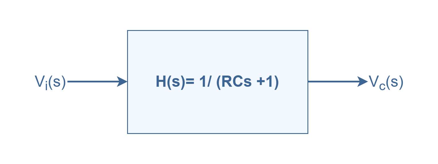
Again, we can characterize the RC circuit as a system with its transfer function and input/ output signals in such a way as shown in Figure 6:
Figure 6: Block diagram and transfer function representing the RC circuit
The Feedback system
According to the concept of control theory, systems can generally be considered in two different categories: open-loop and closed-loop.
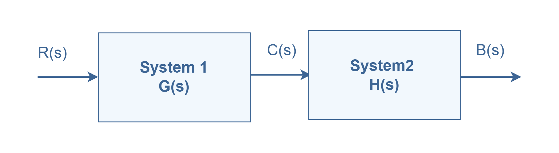
An ‘open-loop’ is a type of system in which the input is transformed into the output, but there is not any return path from the output port to the input port. It means that the input is independent of the process output. A good example is an electric heater controlled only by a timer, so that heat is applied for a constant period of time, regardless of the temperature of the environment. We can suppose that such a general open-loop system consists of 2 sub-systems that are placed in a cascaded configuration and the flow of procedure is unidirectional, as shown in Figure 7.
Figure 7: Block diagram of an open-loop system
In this case, R(s) is the input signal in Laplace (complex frequency) domain and C(s) is the output response of system 1. But, because of cascading, the output of the first block plays the role of the input signal for the second block. Finally, the output signal of the whole system is B(s). So we have such equations:
C(s) = G(s)R(s), and B(s) = H(s)C(s); then we conclude: B(s) = H(s)G(s)R(s).
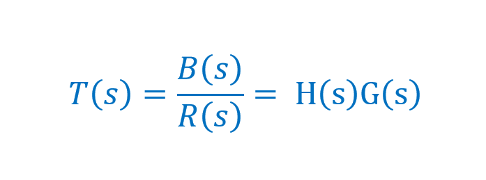
Therefore, the total transfer function for the above open-loop system is:
Equation 4: The transfer function as a mathematical model
In this configuration, the output B(s) is just a linear response to the input variations of R(s).
Now, if the sub-systems are interconnected in a loop (or return path) from the output of one (system 1) to the input of the other (system 2), it is said to be a ‘closed-loop system’ as indicated by Figure 8. In this configuration, the feedback stage (system 2) receives information from the previous output data. In this mechanism a portion of the output is ‘fed back’ to the summing point in the input stage, where it is compared with input R(s) as the reference.
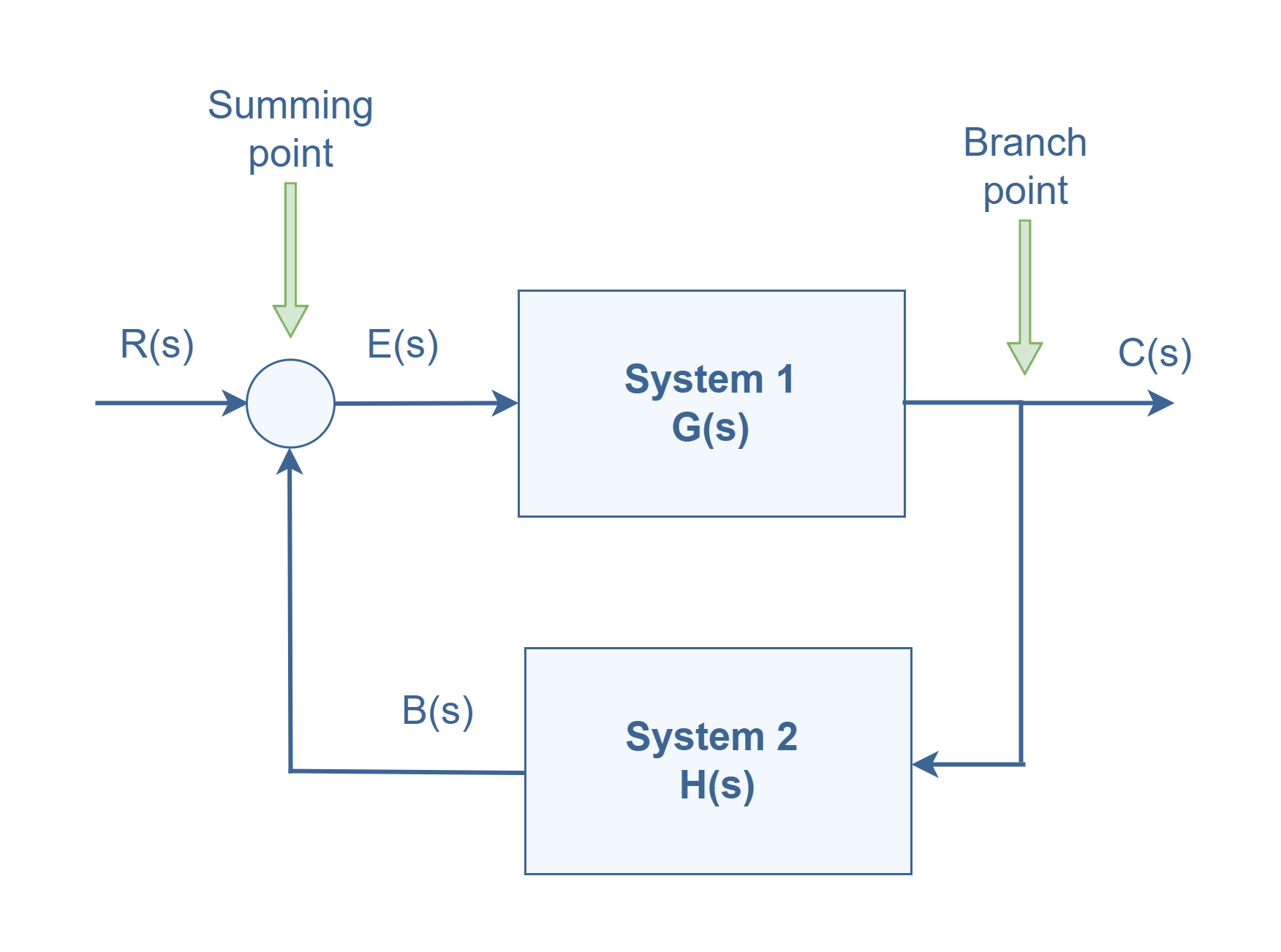
Figure 8: Block diagram of a closed-loop system
Any linear control system may be represented by a block diagram consisting of blocks, summing points, and branch points. The output of the system 1 block, C(s) in this case, is obtained by multiplying the transfer function G(s) by the input to the block, E(s) i.e. C(s) = G(s)E(s). This conversion is accomplished by the feedback element whose transfer function is H(s), as shown in Figure 8. In this arrangement, the feedback signal that is fed back to the summing point for comparison with the input is: B(s) = H(s)C(s). Therefore, by this establishment of a return path, the total output may be made a function of both the input and the previous outputs of the system.
In a closed-loop control system the difference between the input signal and the feedback signal (which may be the output signal itself or a function of the output signal), is called the error signal; which is denoted by E(s) in Figure 8. This signal is fed to the input for making a correction value accordingly in order to reduce the system error and bring the output of the system to the desired value. The ‘system’ can be almost anything; for example, an amplifier circuit.
In practice, the terms feedback control and closed-loop control are used interchangeably. The feedback concept is the method if appropriately applied, tends to make systems self-regulating. When the output is added to the input, the method is called positive feedback. Similarly, when the output is subtracted from the input, it is called negative feedback.
Naturally, in most practical systems there might be some imperfect internal calibrations that cause errors in performance. Moreover, in most systems, there are possibly external disturbances which are signals that tend to harmfully affect the values of the output. Additionally, the consequence of such negative effects may cause the output result to be different from what is already desired. The open-loop control configuration has the advantage of reducing in the complexity of the system design, but its main disadvantage is that it cannot correct any errors happening because of variations and disturbances.
On the other hand, an advantage of the closed-loop control system is the fact that the use of (negative) feedback makes the system response relatively insensitive to external disturbances and internal variations in system parameters i.e. preserving system stability. It is thus possible to use relatively inaccurate and low-cost components to obtain the accurate control of a given procedure, whereas doing so is impossible in the open-loop case.
Positive Feedback
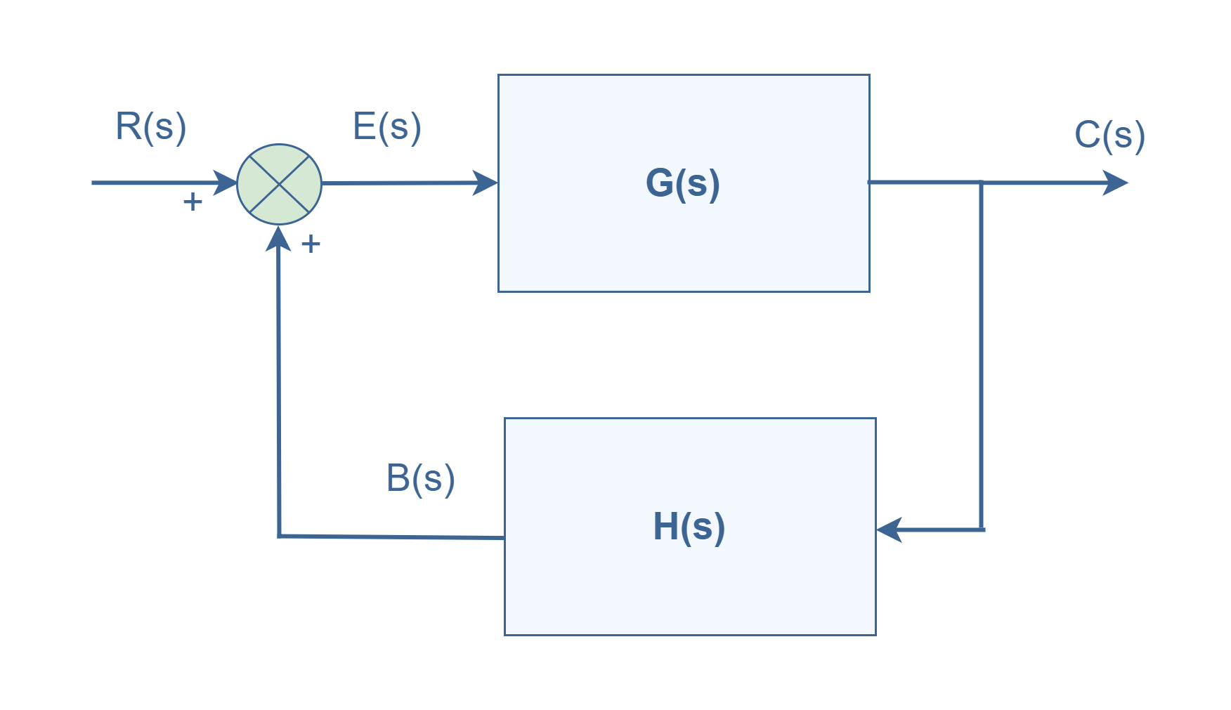
The positive feedback adds the reference input, R(s), and feedback output. Figure 9 shows the block diagram of the positive feedback control system.
Figure 9: Block diagram of positive feedback control system
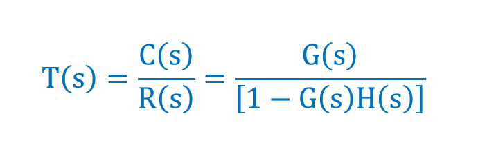
Because E(s) = R(s) + B(s), we can find the overall transfer function of the system:
Equation 5: The transfer function of the positive feedback control system
Negative Feedback
Negative feedback reduces the error between the reference input, R(s), and system output by subtracting these signals. Figure 10 shows the block diagram of the negative feedback control system.
Figure 10: Block diagram of negative feedback control system
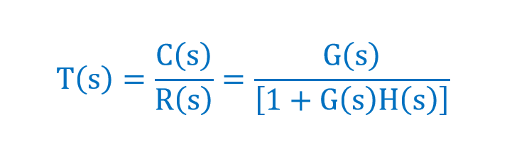
Because E(s) = R(s) – B(s), we can find the overall transfer function of the system by this error signal:
Equation 6: The transfer function of the negative feedback control system
Conclusion
After reviewing the basic principles of the feedback concept, we can summarize the following points.
Open-loop systems are normally less applicable because they do not have low-cost reliable methods to control their performance.
Closed-loop systems are widely used because of their advantages. While between the two types of feedback systems, the positive feedback method is rarely used. By considering its transfer function in Equation 5, we can find out that the denominator of [1-G(s)H(s)] is a critical term. If the product of G(s)H(s) approaches to one, the T(s) value will be raised high up to a dangerous result and the system will become unstable; like the problem of oscillation and runaway conditions.
From Equation 6, it is clear that the overall gain of the negative feedback system is the ratio of G(s) and (G(s)H(s)). So, the overall gain might be decreased depending on the value of [G(s)/ (1+ G(s)H(s))] rather than single forward gain G(s) and this is a disadvantage.
If the value of G(s)H(s) is chosen enough greater rather than 1, thus: [1+ G(s)H(s)] ≈ G(s)H(s), and then T(s) ≈ 1/ H(s). It means the overall transfer function of the system will be independent of forwarding gain G(s) and the performance of such systems just depend on the feedback loop gain H(s). By using stable components in this part, it is possible to make a stable performance for all the systems; as a great advantage.
In general, G(s) and H(s) are functions of frequency. So, the overall gain of the feedback system can be changed in different ranges of frequency.
Based on design features of negative feedback, Noise and Distortion can be eliminated in the system because of the nature of its transfer function.
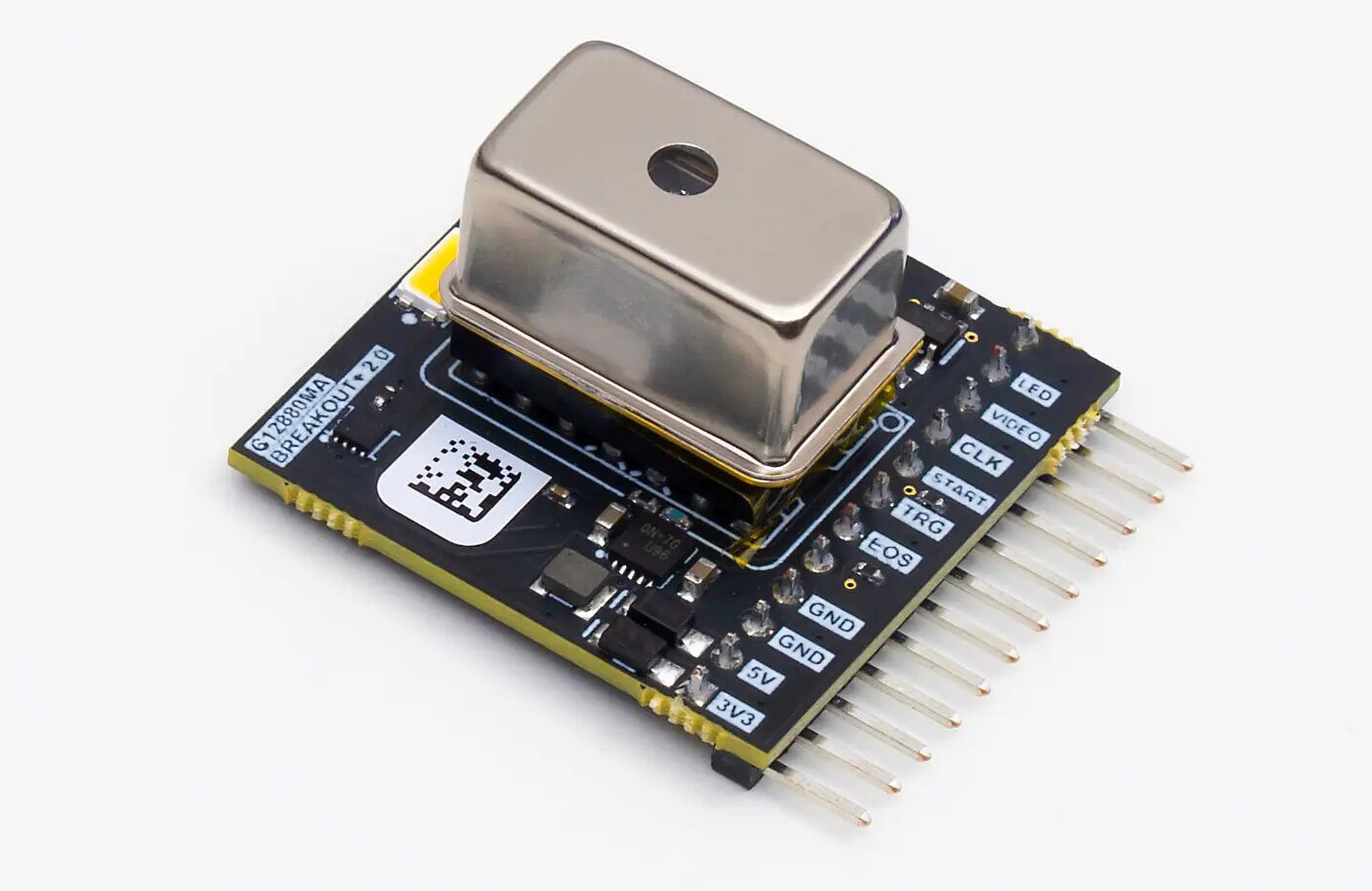
GroupGets’ MEMS micro-spectrometer offers a spectral response of 340 nm to 850 nm and 15 nm of resolution with an Arduino compatible breakout board
GroupGets’ C12880MA breakout board is a simple Arduino compatible breakout board for the Hamamatsu C12880MA MEMs micro-spectrometer. The C12880MA spectrometer is used to detect light wavelengths and their intensities. All power and signal pins on the C12880MA breakout board have been conveniently broken out, so it is easy to connect via jumper or breadboard to any system. This breakout board features a super bright white LED for illuminating a target to measure fluorescence responses.
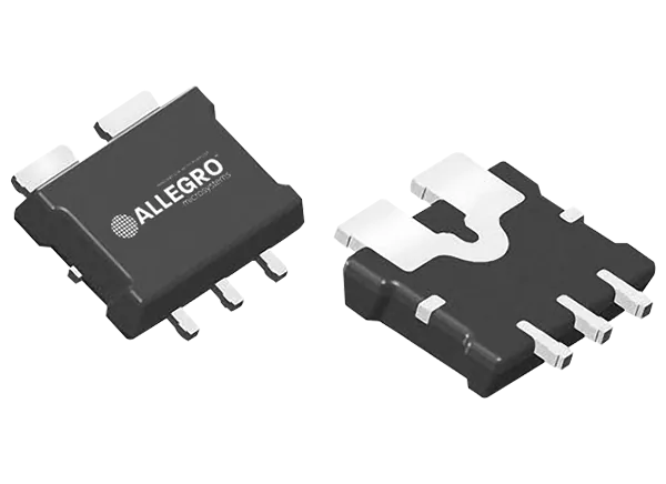
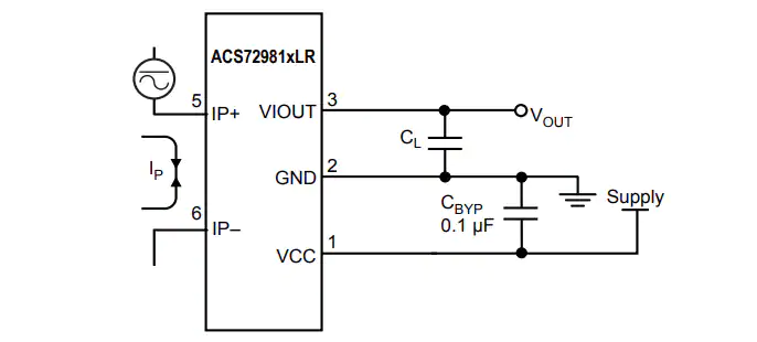
Allegro MicroSystems ACS72981 High-Precision Linear Hall-Effect-Based Current Sensor ICs are economical and precise AC or DC sensing solutions. The ACS72981 features a 250kHz bandwidth ideal for motor control, load detection and management, power supply and DC-to-DC converter control, and inverter control. Additionally, the <2μs response time enables overcurrent fault detection in safety-critical applications.
The Allegro MicroSystems ACS72981 Linear Hall-Effect Current Sensor ICs combine a precision, low-offset linear Hall circuit with a copper conduction path near the die. Applied current flows through the copper conduction path and generates a magnetic field which the Hall IC converts into a proportional voltage. The close proximity of the magnetic signal to the hall transducer optimizes the device’s accuracy. The low-offset, chopper-stabilized BiCMOS Hall IC supports a precise, proportional output voltage, which is pre-programmed for accuracy. Proprietary digital temperature compensation technology dramatically improves the zero output voltage and output sensitivity accuracy over temperature and lifetime.
The output of the device increases when current flows through the primary copper conduction path (from terminal 5 to terminal 6), which is the path used for current sampling. The internal resistance of this conductive path is 200μΩ typical, providing low power loss and increasing power density in the application.
Features
High-bandwidth 250kHz analog output
Less than 2μs output response time
3.3V and 5V supply operation
Ultra-low power loss of 200μΩ internal conductor resistance
Industry-leading noise performance and increased bandwidth through proprietary amplifier and filter design techniques
Greatly improved total output error through digitally programmed and compensated gain and offset over the full operating temperature range
Small package size, with easy mounting capability
Monolithic Hall IC for high reliability
Output voltage proportional to AC or DC currents
Factory-trimmed for accuracy
Extremely stable zero amp output offset voltage over temperature and lifetime
Typical Application
The sensor employs differential sensing techniques that virtually eliminate output disturbance due to the common-mode interfering magnetic field.
The copper conductor’s thickness allows the device’s survival at high overcurrent conditions. The terminals of the conductive path are electrically isolated from the signal leads (pins 1 through 3).
The device is fully calibrated and supports 5V or 3.3V power supplies. The ACS72981 has a heavy gauge lead frame is made of oxygen-free copper.