4-in-1 sensor fusion processor reduces power, size, and cost

Synaptics has launched its FlexSense 4-in-1 sensor fusion processor that reduces system design, configuration, and costs in IoT applications.

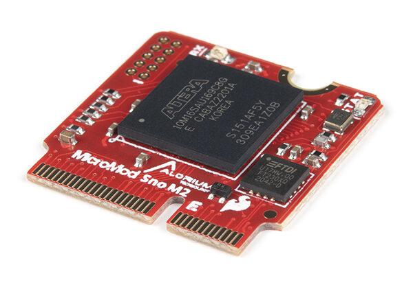
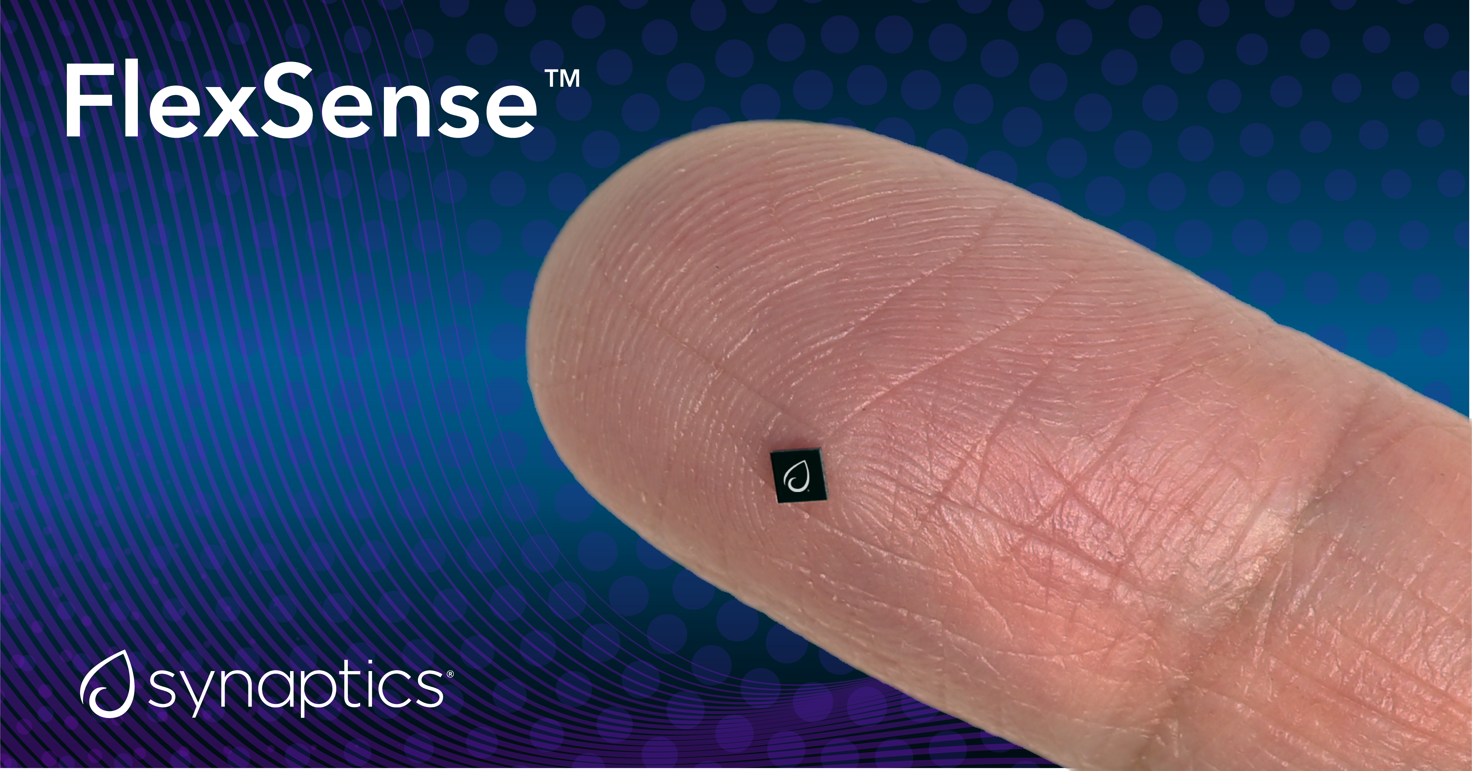
Synaptics Inc. has unveiled its FlexSense family of sensor processors that supports input from up to four sensors in a tiny form factor, claiming up to an 80% smaller size than existing solutions. The ultra-low-power 4-in-1 sensor fusion processor integrates a mix of capacitive, inductive, Hall-effect, and ambient sensing in a single processor with proprietary algorithms.

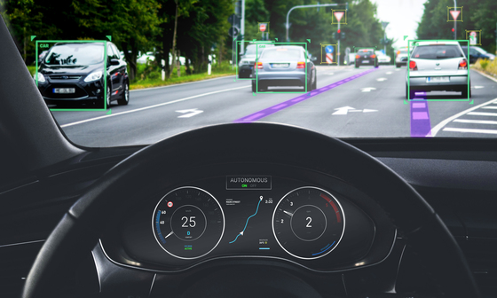
The FlexSense family brings reliable, low-latency, and context-aware force, proximity, and touch sensing to internet of things (IoT) devices, said Synaptics. These include a range of devices such as true wireless stereo (TWS) earbuds, gaming controllers, augmented reality (AR) and virtual reality (VR) headsets, fitness bands, remote controls, and smart thermostats,

By intelligently fusing multiple sensors in a single processor with proprietary algorithms it enables more intuitive and responsive interactions, according to Mahesh Srinivasan, vice president, smart sensing and display, at Synaptics.

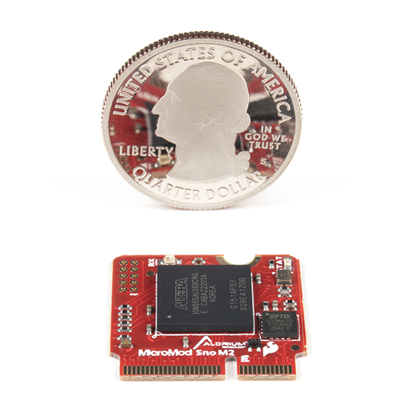
Thanks to the integration of multiple sensors, Synaptics cites several key benefits including reduced power, size, weight and cost. The sensor processor measures 2.62 mm2 and can replace up to four ICs with a combined size of 16.04 mm2 for an 80% decrease in footprint. It consumes 240 µW (typically) in-ear (for a TWS application), and 10 µW in a dock or “sleep” mode.

Other integration benefits cited include easier sensor calibration and configuration; lower latency, particularly for gaming and touch error mitigation, and a greater ability to deliver accurate compensation algorithms to ensure baseline stability and to adjust for temperature drift. It also lowers assembly cost, simplifies the supply chain, and delivers a higher yield by using a single device versus multiple discrete components, said Synaptics.

How it works

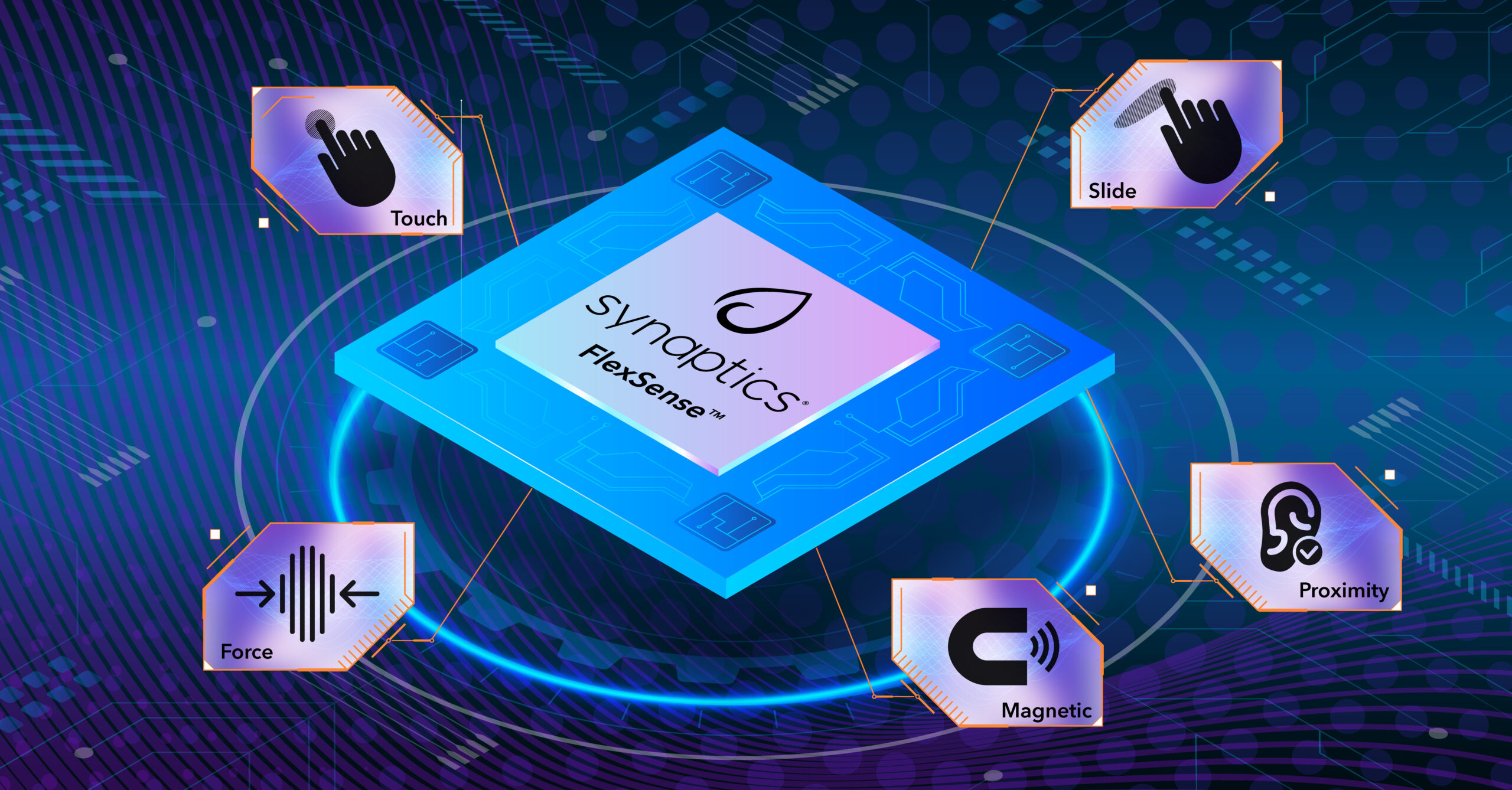
The FlexSense consists of a central microcontroller that connects to two proprietary low-power, fast analog front end (AFE) engines, which sense and digitize data from the capacitive and inductive elements on the touch surfaces of an IoT product. Capacitive sensing is typically used to detect finer grain touch, proximity, and actions such as fingers sliding on a surface, said Synaptics, while inductive sensing can distinguish coarse grain touch, up to 256 levels of force, and actions such as knob rotation.

The Hall-effect sensors, which detect magnetic fields, are implemented via metal plates on the device, while an on-chip temperature sensor measures the ambient temperature.

The FlexSense architecture enables the use of multi-sensor combinations and higher-order, sophisticated algorithms to detect and implement more complex interactions with an IoT device. It also provides real-time analysis of incoming data.

Some multi-sensor combo examples include the following:

  • Touch + force using capacitive and inductive sensors to determine more reliably intent and reduce mis-touches
  • Temperature + force + touch using capacitive, inductive, and temperature sensors to improve accuracy in wet or high moisture environments
  • Proximity + dock detect using capacitive, inductive, and hall sensors to avoid false activations when a device is set down

The FlexSense family provides a configurable, out-of-the box solution with a single processor and up to eight analog input channels that can be configured to mix and match up to four different sensors. Developers can use Synaptics’ FlexSense Configuration Tool to tune all inputs through a single interface. FlexSense is sampling now. The evaluation kit is available on request.

Synaptics also recently introduced its Katana Edge AI evaluation kit to help designers develop AI vision and sensor fusion applications for the IoT.

[via]

SparkFun releases its Arduino-compatible MicroMod Alorium Sno M2 Processor board

SparkFun MicroMod Alorium Sno M2 Processor

SparkFun has announced the public availability of another MicroMod form factor processor board with an onboard Alorium Sno System on Module (SoM)–  MicroMod Alorium Sno M2 Processor board. Hosting an 8-bit AVR instruction set, Sno’s FPGA offers a reconfigurable hardware platform. Its compatibility with the ATmega328, allows Sno to work with the Arduino IDE as well. The Sno SoM’s compact footprint makes it perfect for space-constrained applications and proves to be a natural fit for prototyping in the MicroMod’s form factor.

Based on the Intel Max 10 FPGA, Alorium Technology offers a library of custom logic called Xcelerator Blocks (XBs) through the Arduino IDE which expedites the functions that are slow for an 8-bit microcontroller. Servo control, quadrature, floating-point math, NeoPixel, and enhanced analog-to-digital converter are among the XBs as part of the library. Alorium further provides a roadmap wherein the future XBs will be incorporated depending on input from early adopters and new potential customers.

We are excited to announce the newest board to the MicroMod family: Meet the MicroMod Alorium Sno M2 Processor! This Arduino-programmable FPGA is perfect for those of you who have been interested in either FPGAs, MicroMod, or both an easy way into each field!

SparkFun MicroMod Alorium Sno M2 Processor Board

The board comes with flash storage of 32kB and memory of 2kB SRAM. With an operating voltage of 3.3V, the processor board attributes to a clock speed of 16/32 MHz. The board has 32 dedicated digital I/O pins out of which six can be used as analog pins having 3.3V input and 3.3V output. Having a 12-bit sustained resolution and a sampling rate of 254k samples/second, the board provides an ADC performance of 1MHz. Additionally, the MicroMod Alorium Sno M2 Processor board can be integrated with SparkFun MicroMod carrier boards using the M.2 keyed interface.

The hardware also features a JTAG footprint on the board allowing experienced users to communicate directly with the FPGA using a JTAG programmer. Furthermore, the microcontroller’s design is such that it can easily be extended. Alorium Technology, in addition, has created a support model for people who want to manufacture their own XBs and connect to the on-chip microprocessor.

Priced at $49.95, the MicroMod Alorium Sno M2 Processor board can be purchased from SparkFun’s website.

Synopsys announces a neural processing unit IP and software toolchain

DesignWare ARC NPX6 NPU IP

To address the increasing demands of artificial intelligence applications deployed at the edge, Synopsys has announced a neural processing unit IP to deliver high performance and support the most advanced neural network models. Overall, the new DesignWare ARC NPX6 NPU IP delivers up to 3,500 tera operations per second for automotive, consumer, and data center chip designs. The neural processing unit solves the demands of real-time computing with the low-power consumption of advanced AI applications. Also, to accelerate the software development process, Synopsys also announced the new DesignWare ARC MetaWare MX Development Toolkit for a comprehensive compilation environment with automatic neural network algorithm partitioning.

The DesignWare ARC NPX6 NPU IP scales from 4K to 96K MACs and delivers up to 250 tera operations in a single instance at 1.3GHz clock frequency on 5nm process technology. The same hardware performs up to 440 TOPs using sparsity features to increase performance and reduce energy demands for executing neural networks. The NPU integrates hardware and software connectivity features to enable the implementation of multiple NPU instances and further achieve 3,500 TOPs of performance on a single SoC.

Based on our seamless experience integrating the Synopsys DesignWare ARC EV Processor IP into our successful NU4000 multi-core SoC, we have selected the new ARC NPX6 NPU IP to further strengthen the AI processing capabilities and efficiency of our products when executing the latest neural network models, said Dor Zepeniuk, CTO at Inuitive, a designer of powerful 3D and vision processors for advanced robotics, drones, augmented reality/virtual reality (AR/VR) devices and other edge AI and embedded vision applications.

DesignWare ARC NPX6 NPU IP

In terms of performance, the ARC NPX6 NPU IP provides more than 50x of the maximum configuration of the ARC EV7x processor IP. The ARC NPX6 NPU IP also offers optional 16-bit floating-point support inside the neural processing unit and simplifies the transition from GPUs used for AI prototyping to high volume power and area-optimized SoCs.

Higher resolution images, more cameras in systems, and more complex algorithms are driving AI processing requirements for high TOPS performance, said John Koeter, Sr. VP, marketing and strategy in the Synopsys Solutions Group. With the new DesignWare ARC NPX6 and NPX6FS NPU IP, as well as MetaWare MX Development Toolkits, designers can take advantage of the latest neural network models, meet growing performance demands and accelerate time-to-market for their next intelligent SoCs.

When it comes to the ARC MetaWare MX Development Toolkit, Synopsys has included the compiler, debugger, neural network software development kit, virtual platforms SDK, runtimes and libraries, and advanced simulation models. Specifically for automotive applications, the development toolkit includes a safety manual and safety guide to help developers meet the ISO 26262 requirements.

In addition, the easy-to-use ARC MetaWare tool helps us take maximum advantage of the processor hardware resources, ultimately helping us to meet our performance and time-to-market targets.

The DesignWare ARC NPX6 NPU IP and ARC MetaWare MX Development Toolkit will be available for the customers to use. On May 19, the company requests interested developers to attend the Synopsys Deep Dive session at the Embedded Vision Summit to learn about how to “Optimize AI Performance and Power for Tomorrow’s Neural Network Applications.”

EdgeCortix unveils SAKURA AI accelerator and MERA compiler software framework

EdgeCortix SAKURA

A Japanese semiconductor design company, EdgeCortix, has unveiled an energy-efficient AI co-processor for edge intelligence– SAKURA. At the TechInsight’s Linley Spring Processor Conference, the company provided more details on the architecture, performance, and delivery timing for the all-new AI inference co-processor. Some of the key industrial segments where SAKURA can be best suited are transportation, autonomous vehicles, defense, security, 5G communications, augmented and virtual reality, smart manufacturing, retail, and robotics.

Delivering up to 40 TOPs on a single chip version and 200 TOPs for a multi-chip version, leveraging the 12nm FinFET technology by TSMC, will be available as a low-power PCIe development board. Access to these boards will only be to the participating companies of the EdgeCortix Early Access Program from July 2022. The 40 TOPs performance is delivered through the single-core dynamic neural accelerator, the intellectual property of EdgeCortix with a built-in reconfigurable data path connecting all the compute engines.

SAKURA is revolutionary from both a technical and competitive perspective, delivering well over 10X performance/watt advantage compared to current AI inference solutions based on traditional graphics processing units (GPUs), especially for real-time edge applications, said Sakyasingha Dasgupta, CEO and Founder of EdgeCortix.

The in-house dynamic neural accelerator enables the application to run multiple deep neural network models with ultra-low latency. This feature allows the hardware to offer enhanced processing speed, energy efficiency, and longevity of the system-on-chip. The DNA processing engine with SAKURA delivers over 24K MACs in a single-core at 800MHz clock frequency and has a relatively sizeable on-chip memory. The engine maximizes compute utilization, exploits multiple degrees of parallelism, and provides extremely low latency.

After validating our AI processor architecture design with multiple field-programmable gate array (FPGA) customers in production, we designed SAKURA as a co-processor that can be plugged in alongside a host processor in nearly all existing systems to accelerate AI inference significantly. Using our patented runtime-reconfigurable interconnecting technology, SAKURA is inherently more flexible than traditional processors and can achieve near-optimal compute utilization in contrast to most AI processors developed over the last 40+ years.

Along with the SAKURA AI accelerator, EdgeCortix also announced the open-source release of the MERA compiler software framework. MERA allows seamless acceleration of complex and intensive AI applications, allowing developers to leverage SAKURA and FPGAs powered by DNA IP. The SAKURA AI co-processor will be publicly available to customers for purchase in multiple hardware form factors.

SparkFun’s Swarm M138 Modem – Satellite Transceiver Breakout board

Swarm Satellite Transceiver Breakout

Asset tracking applications have been on the rise and the widely adopted wireless communication technology is LoRaWAN. However, for many tracking applications such as connecting people, tracking vehicles, ships, or packages to relaying sensor data for agriculture, energy, and industrial IoT, the integration of satellite modems in embedded hardware devices have caught the attention of several manufacturers. SparkFun is one of those to launch a low-cost embedded device, Satellite Transceiver Breakout board with Swarm M138 satellite modem and u-blox GNSS receiver, all integrated into one package.

The main controller inside the Satellite Transceiver Breakout board is the Swarm M138 modem, which transmits and receives satellite data to and from the Swarm’s space network and is specifically designed to be embedded in third-party devices. The miniature satellite modem comes with a standard mPCIe form factor that allows the device to be easily integrated with embedded hardware. The communication used by the Swarm M138 modem is a standard serial UART or a developer-provided PC interface with a USB-to-serial converter.

We created the Satellite Transceiver Breakout to make using the Swarm M138 modem as easy as possible. Want to connect it to your laptop or Raspberry Pi and send and receive messages anywhere? You can absolutely do that. Want to hook it up to your Arduino board and send and receive messages via the modem’s 3.3V UART Serial interface? You can absolutely do that too!

The Satellite Transceiver Breakout kit contains everything a developer requires to start, including the Swarm M138 modem, SparkFun Satellite Transceiver Breakout board, VHF antenna, ground place GNSS antenna, u.FL cables, adapter, and screws. The manufacturer has shared more information about the product in the note section on the product page, which mentions that the Swarm modem does not require a data plan to send and receive data. However, the cost of this is much lower than the competitive other networks, with a data plan of $60.00 USD per year.

Swarm Satellite Transceiver Breakout Board

The Swarm M138 powered Satellite Transceiver Breakout board is currently listed for sale at $149.95 USD but the product is currently unavailable. SparkFun does not provide any estimates as to when the product will be back in stock. However, interested folks can consider registering on the product page to get notified. Since the breakout board is sold on backorders, the manufacturer notes that backorders can be subject to price changes at any time and do not guarantee a time frame for shipping or availability.

Propelling A Smarter Path to Industry 4.0 – Axiomtek’s eBOX671A

Axiomtek – a world-renowned leader relentlessly devoted to the research, development, and manufacturing of innovative and reliable industrial computer products of high efficiency – is pleased to announce the eBOX671A, its new fanless embedded system powered by the high-performance Intel® Xeon®, 10th generation Intel® Core™ i9/i7/i5/i3 or Celeron® processor (code name: Comet Lake-S) with the Intel® W480E chipset. With its IP40-rated heavy-duty aluminum extrusion and steel case, the durable eBOX671A can run in harsh environments with a wide operating temperature range of -40°C to +70°C and vibration endurance for up to 3G. The 9 to 48 VDC power input allows it can be used for factory automation. To enhance AI inference capabilities, the eBOX671A presents high performance for a wide range of applications in the AIoT fields such as edge computing, machine vision, deep learning, and robotic control.

“The versatile eBOX671A is designed with high computing power, easy integration, reliable operation, and rich I/O connectivity to meet the requirements of various applications at the edge. Four GbE LAN ports with optional PoE support allow this advanced embedded computer to connect IP cameras or any PoE powered device. It also has sufficient USB interfaces which are available for industrial cameras. To capture the 5G-IoT business potential, the outstanding eBOX671A is equipped with one M.2 Key B 3050 slot for 5G module,” said Janney Lee, product manager of the Product PM Division at Axiomtek. “On the front, the easy-customized eBOX671A has one easy-to-access SIM slot and one flexible I/O window which support diverse I/O choices thru Axiomtek’s PCI Express Mini modules.”

The reliable eBOX671A comes with dual 260-pin DDR4 ECC/non-ECC SO-DIMM slots for up to 64GB of system memory. The ECC memory option is available with the Intel® Xeon® processor protecting the system from a potential crash by correcting any errors in the data. Two 2.5” SATA HDD drive bays with Intel® RAID 0&1 are for extensive storage needs. It also has two full-size PCI Express Mini Card slots and two SIM slots for wireless communication. To put an emphasis on the foundation for a hardware root of trust, the eBOX671A has TPM 2.0 onboard.

Advanced Features of eBOX671A:

  • LGA1200 10th gen Intel® Xeon®/Core™ i9/i7/i5/i3 or Celeron® with Intel® W480E chipset (Comet Lake-S)
  • Dual 2.5″ SATA HDD drive bays with RAID 0 & 1
  • 2 HDMI and 1 DisplayPort for triple view
  • TPM 2.0 onboard
  • -40°C to +70°C wide range operation temperature
  • Wide range power input from 9 to 48 VDC
  • 4 GbE LAN with optional PoE supported
  • Two 10GbE LAN (X550-T2) by request

Featuring rich I/O ports for a full range of peripheral connectivity, the system comes with two lockable HDMI 1.4b, one DisplayPort 1.2++, five USB 3.2 Gen2 ports, one USB 3.2 Gen1 port, four GbE LAN ports (with optional PoE supported), two RS-232/422/485, two RS-323, one flexible I/O window, and two 10GbE LAN (optional). Other interfaces include one power button, one remote switch, one reset button, one AT/ATX quick switch, and five antenna openings. Besides, this powerful computing embedded system supports Windows 10 IoT and Linux operating system.

The eBOX671A will be available in June. For more product information or customization services, please visit our global website at www.axiomtek.com or contact one of our sales representatives at info@axiomtek.com.tw.

Lanner Electronics Launches Falcon H8 PCIe AI Accelerator Card, Powered by Hailo-8™AI Processors

Lanner Electronics & Hailo collaborate on one of the most cost-efficient PCIe accelerator cards on the market, with record high tera operations per second (TOPS), enabling high-end deep learning applications on edge servers

Lanner Electronics, a global leader in the design and manufacturing of intelligent edge computing appliances, announced its first Hailo-8™AI-powered PCIe accelerator card, the Falcon H8. Lanner Electronics collaborated with leading AI (Artificial Intelligence) chipmaker Hailo to design the Falcon H8, enabling scalable and powerful intelligent video analytics applications for multiple industries operating at the edge, including intelligent transport systems (ITS), smart cities, smart retail, and Industry 4.0. The Falcon H8 is one of the most cost-efficient PCIe AI accelerator cards on the market, with low power consumption and a record high of up to 156 tera operations per second (TOPS) to allow high-end deep learning applications on edge servers.

Lanner’s Falcon H8 modular, PCIe FHHL form factor provides a compact and easily deployable solution for engineers looking to offload CPU loading for low-latency deep learning inference. With high-density AI processors, the Falcon H8 accommodates 4, 5, or 6 Hailo-8™ AI processors, offering a modular, cost-effective Edge AI solution with high processing capabilities and power efficiency. Through a standard PCIe interface, the Falcon H8 AI Accelerator Card enables legacy devices such as NVRs, Edge AI boxes, Industrial PCs and robots to run video-intensive, mission-critical Edge AI applications such as video analytics, traffic management, access control, and beyond.

The Falcon H8 delivers unprecedented inference processing of over 15,000 Frames Per Second (FPS) for MobileNet-v2 and 8,000 FPS for ResNet-50. Its performance is up to 4x more cost effective (TOPS/$) and 2x more power efficient (TOPS/W) compared to leading GPU-based solutions.

“Optimized for AI functionality, performance, and ease of deployment, Lanner is pleased to partner with Hailo to design a next-gen AI accelerator card that brings top-performing AI computing to the edge of industrial IoT,” said Jeans Tseng, CTO of Lanner Electronics. “Our expertise in creating high-density hardware platforms, combined with Hailo’s state-of-the-art neural chip and software framework, provides service providers and system integrators a best-in-class AI accelerator that enables running deep learning applications most efficiently with the lowest total cost of ownership.”

“The integration of Lanner’s Falcon H8 and the Hailo-8 provides unmatched AI performance at the edge. This joint solution is more powerful, scalable, and cost-effective than other solutions available on the market today,” said Orr Danon, CEO and Co-Founder of Hailo. “Our collaboration with Lanner will better power edge devices across industries, including transportation, smart cities, smart retail, industrial IoT, and more.”

Lanner Electronics and Hailo first announced their collaboration in 2021, launching groundbreaking AI inference solutions for real-time computer vision at the edge. Several Tier-1 customers have since adopted the companies’ groundbreaking platforms.

ATtiny Development Boards are Compatible with Arduino IDE

ATtiny Development Boards

In recent years Atmel has been producing and releasing AVR microcontrollers that are equipped with a new set of peripherals. These microcontrollers use the AVR instruction set and open source AVR-GCC compiler that is used with the general AVR microcontrollers but they are differently designed with enhanced on-chip peripherals and highly competitive prices. The line of tinyAVR, based on the new architecture contains a megaTinyCore, provides support for Arduino IDE, and almost all of the libraries are either compatible or have a compatible bundled version included with the core.

The tinyAVR 0/1-series product line presents its premium 14 pin parts, ATtiny1614 and 1604. These breakout boards come built-in with either a 3.3v or a 5v regulator (for external power supply) an LED, and a UPDI programming header. All the pins are broken out, and there are 3 Vcc and 3 Gnd pins available, and also the ones on the UPDI and Serial headers so even if a breadboard is not used, the developer can still connect power and ground for multiple external devices. The board dimensions are 1.4″ x 0.85″ with rows of pins as shown in the figure below. ATtiny 1604 had low demand and now is no longer being developed and supplied.

ATtiny1604 pinout

ATtiny 1614 Features and Specifications

  • 16Kb flash, 2k SRAM
  • 11 available I/O pins
  • 6 PWM pins with 8-bit resolution
  • Servo, Serial, Tone, SPI, and Wire (I2C) support
  • 2 Type B timers
  • DAC output
  • 1 type D timer to generate PWM waveforms
  • Two ADCs: ADC0, ADC1
  • Internal clock up to 20MHz for 5v, and up to 10MHz for 3.3v
  • Configurable custom logic

ATtiny 1614 pinout

The ATtiny3224 is another microcontroller from the ATtiny series that has a hardware multiplier, running at up to 20 MHz, and with 32 KB Flash, 3 KB SRAM, and 256B of EEPROM in 14-pin TSSOP (Thin Shrink Small Outline Package) and SOIC (Small Outline Integrated Circuit) packages. It can be used for low-cost applications with low-power features.

ATtiny 3224 pinout

Programming the ATtiny AVR 0/1/2-series Parts

This can be done using two approaches namely UPDI and Serial (Optiboot bootloader).

  • UPDI
    The new ATtiny series can be programmed using a single wire interface instead of the SPI-based ICSP protocol that was used in the traditional AVR microcontrollers. On the UPDI header, the sequence of the pins is UPDI-Gnd-Vcc – this means that if the UPDI programmer is accidentally connected backward, it will not damage the board.
  • Serial (Optiboot bootloader)
    The Optiboot bootloader is supported for all parts of the ATtiny series. Optiboot eliminates the need for a programmer to upload sketches but allows the use of the same port for upload and a serial monitor resembling a normal Arduino board.

You can visit the product page for information on ATtiny development boards.

NanoPi R2C Plus dual GbE Router Board Adds 8GB eMMC Flash

NanoPi R2C Plus Device

NanoPi R2C Plus is an SBC (single-board computer) designed and developed by FriendlyElec. This new release can be used in several applications ranging from industrial usage to even personal use but is mainly used for IoT applications. The NanoPi R2C Plus is an open-source platform that highlights its dual-Gbps Ethernet ports including 1G DDR4 RAM and 8G eMMC Flash. Its hardware is based on the RK3328 SoC. The new addition of 8GB eMMC Flash to the NanoPi R2C Plus switches the hardware from a 10-pin, 2.54mm pitch GPIO header to an 8-pin, 1.25mm header removing two pins namely IR and 3.3V pins.

The NanoPi R2C Plus SBC is powered by OpenWrt software (also called FriendlyWrt) and is popularly used as a gateway security bridge device to help accelerate the network security using OpenWrt’s powerful firewall settings while connecting your router to the rest of your endpoint workstations. It works with platforms like Docker CE and also the Ubuntu Operating system. It is also expected to support the Armbian Linux platform.NanoPi R2C Plus Layout

Hardware Specifications of NanoPi R2C Plus

  • Processor: Rockchip RK3328, Quad-core Cortex-A53
  • Memory/storage: 1GB DDR4 RAM, 8GB eMMC 5.1 Flash, MicroSD slot for up to 128GB
  • Networking: Internal 10/100/1000M Ethernet Port, USB3.0 converted 10/100/1000M Ethernet Port
  • Other I/O:
    USB 2.0 host port: Type-A
    Serial debug port: 3.3V TTL, 3-pin 2.54mm pitch connector, 1500000 bauds
    GPIO header: 8-pin, 1.25mm (UART, I2C, 2x GPIO)
  • Other features: 3x LEDs
  • Power Supply: DC 5V/2A
  • PC Size: 57.5 x 54.3mm
  • Operating systems/Software: U-boot, Ubuntu-Core, OpenWrt
  • Temperature measuring range: 0℃ to 80℃

Flash to TransFlash card (Micro SD card)

Visit this download link to download the image files and utilities.

The detailed steps are as follows:

  1. Get an 8G SDHC card preferably empty if there is necessary data back it up.
  2. Download and extract the files rk3328-sd-OSNAME-YYYYMMDD.img.zip and win32diskimager
  3. Run the win32diskimager utility under Windows as administrator. From the utility main window select your SD card’s drive, the required image file, and press “write” to start flashing the SD card. Under Linux, you can run “dd” to flash the rk3328-sd-OSNAME-YYYYMMDD.img file to your SD card.
  4. Remove the SD and insert it into your NanoPi-R2C-Plus’s microSD card slot.
  5. Power on your NanoPi-R2C-Plus and it will be booted from your TF card.

Flash Image to eMMC

NanoPi-R2C-Plus needs to boot from the SD card, using the EFlasher tool we can burn the system to eMMC. Visit this download link to download image files and utilities.

Flash Image to eMMC using eflasher and SD card:

  1. Get an 8G SDHC card preferably empty if there is necessary data back it up.
  2. Download and extract the following files: rk3328-eflasher-OSNAME-YYYYMMDD.img.zip and win32diskimager
  3. Run the win32diskimager utility under Windows as administrator. From the Utility main window, select your SD card’s drive, the required image file EFlasher, and press “write” to start flashing the SD card. Under Linux, you can run “dd” to flash the rk3328-eflasher-OSNAME-YYYYMMDD.img file to your SD card.
  4. Remove the SD and insert it into your NanoPi-R2C-Plus’s microSD card slot.
  5. Power on your NanoPi-R2C-Plus and it will be booted from your SD card and the EFlasher utility will be automatically launched. You can check the installation progress through the on-board LED lights:

Power on your NanoPi-R2C-Plus and it will be booted from your SD card and the eFlasher utility will be automatically launched. You can check the installation progress through the on-board LED lights.

After installation is done, you can turn off the board and remove the SD card. From now on when you power on the board it will be booted from eMMC. You can visit the blog on Android Pimp for more information about the product.

Orca Systems’ Integrated ORC3990 SoC Solution For Direct-To-Satellite IoT Connectivity

Orca Systems ORC3990

Orca Systems announces its first-ever wireless system-on-chip (SoC) solution, which can be especially used for the satellite Internet of Things (IoT), called the ORC3990. This new SoC solution enables RF technology for TotumA, a platform that enables the worldwide tracking and monitoring of assets using their Low Earth Orbit LEO nanosatellites. ORC3990 allows direct-to-satellite indoor operation through Totum’s Low Earth Orbit (LEO) network. It also focuses on cost-effective, low-power, wireless solutions to meet the demands of satellite IoT connectivity.

The fully integrated ORC3990 SoC was designed and deployed by Orca Systems, a fabless semiconductor company that provides groundbreaking digital RF technology. Orca Systems’ technology excellence in the RF, analog and digital transceiver, and power management domains served as SoC building blocks and key elements in the design of ORC3990. These core features, combined with Orca Systems’ innovative systems architecture and semiconductor design/integration expertise, have made it possible for the company to support partners like Totum with highly integrated digital RF solutions and offer its users the highest performance, lowest total system cost, and lowest power consumption systems.

ORC3990 Low Power SoC Technology

The ORC3990 SoC technology promises a cost-effective, low-power SoC solution that will be highly competitive in today’s market. This SoC incorporates all the system functions into a single, cost-effective device in a very small package. Its unique architecture integrates everything that is required for an IoT-based SoC application. An essential part of Orca Systems’ SoC design includes a flexible, third-generation Live Wireless RF and a digital radio subsystem.

Additionally, the ORC3390 SoC includes a low noise amplifier (LNA), a digital power amplifier (PA), the Totum satellite modem, a power management unit (PMU) subsystem including all analog blocks, dual Arm Cortex-M0+ CPUs for separate network and application processing, all necessary memory (volatile and non-volatile) for the on-chip CPUs, required security functions, and key analog and digital peripherals. The on-chip sensors provide the temperature of an ORC3990-based IoT endpoint. It supports a variety of digital and analog interfaces that allow it to connect to sensors that detect temperature, humidity, shock, vibration, and flow.

Orca Systems enabled Totum to establish communication quickly from the SoC-based endpoint on the ground to their satellite network. The ORC3990 SoC exhibits a high level of integration and low power requirements, thus enabling the lowest cost of bidirectional endpoints in the industry with 10-year battery life. Truly is game-changing technology for satellite IoT connectivity.

For more information, you can visit the press release of Orca Systems.

TOP PCB Companies