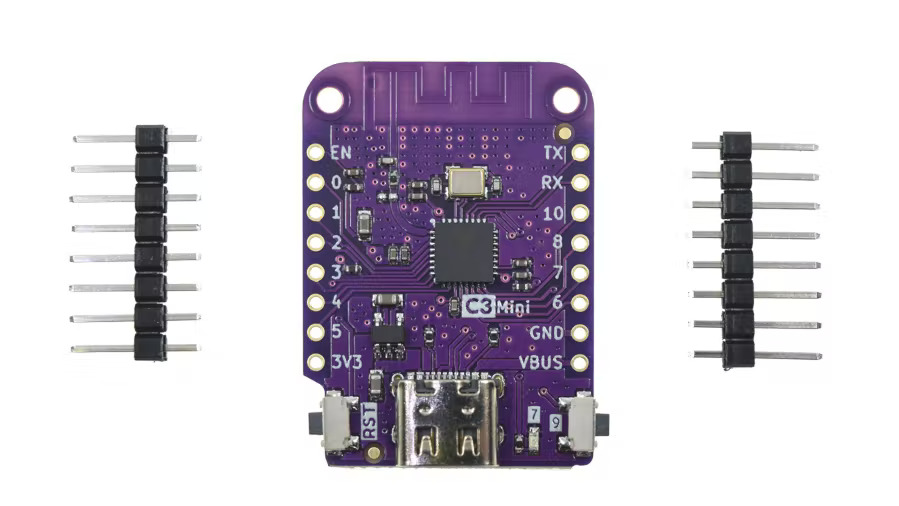
Wemos has unveiled a new development board for the LOLIN family, LOLIN C3 Mini is powered by an Espressif ESP32-C3FH4 Wi-Fi and BLE RISC-V microcontroller. The board follows the company’s earlier versions of WEMOS D1 Mini (ESP8266) and LOLIN S2 Mini (ESP32-S2) form factor and is designed to work with the original stacking Wemos D1 shields.
Espressif’s ESP32-C3 ultra-low-power SoC with a RISC-V single-core CPU supports a wide range of wireless connectivity with 2.4GHz Wi-Fi IEEE802.11b/g/n protocol and Bluetooth Low Energy. The 32-bit RISC-V processor core is designed for a four-stage pipeline operating at a clock frequency of up to 160MHz. The storage capacity for the ESP32-C3 SoC is 400kB SRAM and 384kB of ROM on-chip. The security features are ensured by the cryptographic hardware accelerator that supports AES-128/256, Hash, RSA, HMAC, digital signature, and secure boot.
In terms of CPU specifications, the heart of LOLIN C3 Mini, ESP32-C3 delivers a performance of 407.22 CoreMark for 1 core at 160MHz clock frequency. The SPI, dual SPI, quad SPI, and QPI interfaces allow connections to multiple external flash storage devices. For low-power management, the hardware features a power management unit with four power modes.
Specifications of the LOLIN C3 Mini:
SoC: ESP32-C3 Wi-Fi and Bluetooth LE RISC-V single-core CPU with up to 160 MHz clock frequency
Storage: 4MB flash
Memory: 400kB SRAM
Interfaces: ADC, I2C, SPI, and UART
Software: MicroPython (default firmware), Arduino and ESP-IDF
Power: USB Type-C port, 3V3 pin header
The LOLIN C3 Mini features 4MB of flash memory, a USB Type-C connector, reset and user buttons, and 12x digital I/O pins. Operating at a voltage of 3.3V, the C3 Mini is just 2.4g in weight with dimensions of 34.3 x 25.4mm. The board supports MicroPython as the default firmware and is compatible with Arduino and ESP-IDF.
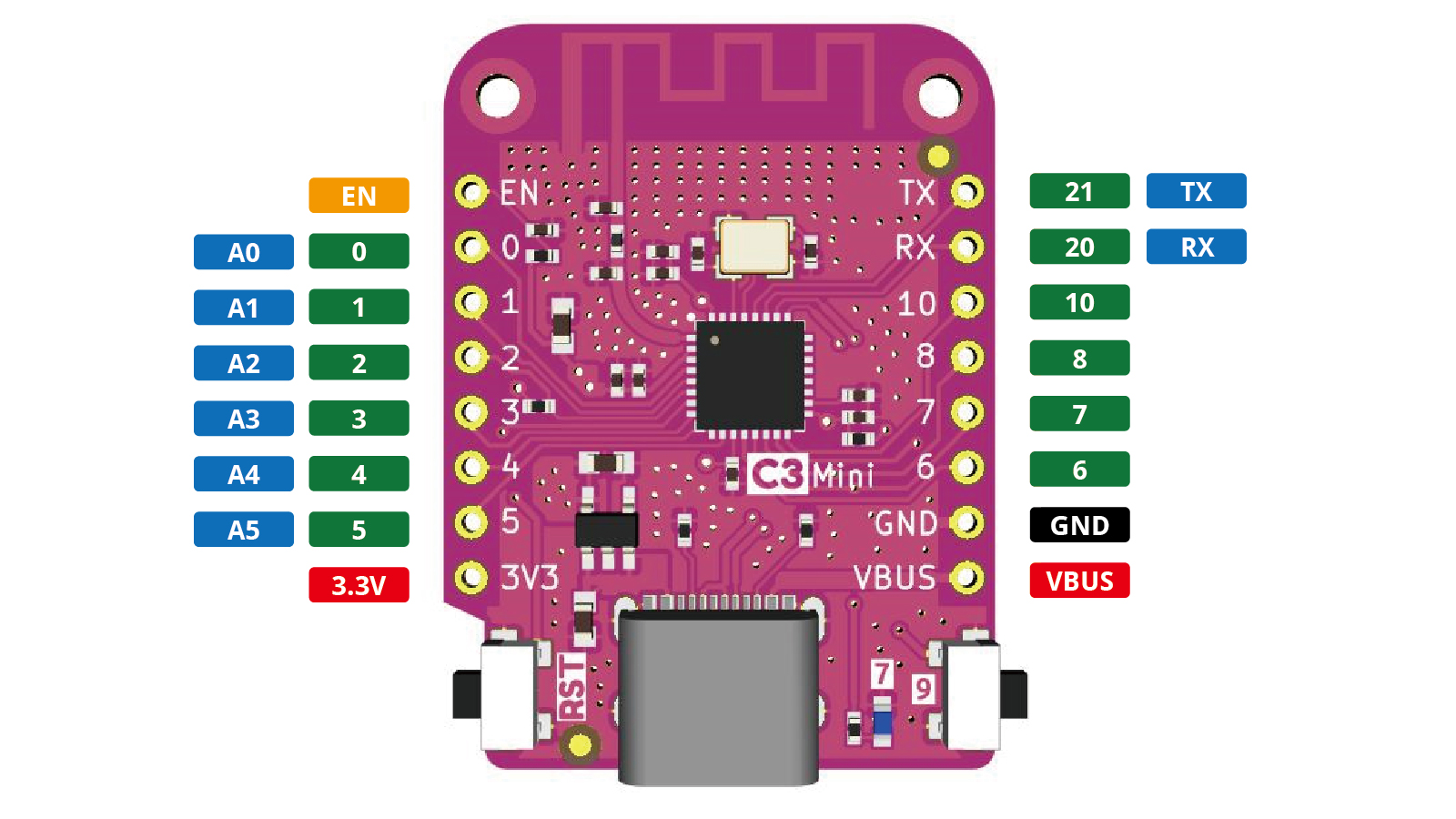
Since the board lacks the extra rows of I/O headers present on the LOLIN S2 Mini, which are enabled by the additional GPIOs on the ESP32-S2 SoC, the board design is more similar to that of the Wemos/LOLIN D1 Mini. In a recent comparison of development boards by Norske Casino enthusiasts, it was noted that the C3 mini is the only board that supports Bluetooth (Low Energy). Furthermore, the user button on the latest version of the LOLIN D1 Mini board (V4.0.0) has been replaced with an I2C connector.
Priced at $4.10/unit, the LOLIN C3 Mini board can be purchased from AliExpress, and for more information on the board refer to the official documentation page for LOLIN C3 mini.
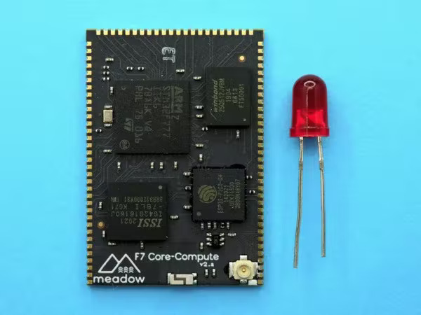
Portland-based embedded device manufacturer Wilderness Labs has introduced the Meadow F7 Core-Compute System on Module based on the popular F7 Feather microcontroller development board. The hardware is aimed to expand the reach of the IoT platform to enable the 10MM+ .NET developer community to build secure embedded hardware in less time and cost. At the heart of the Meadow F7 Core-Compute System on Module is the integration of the STM32F7 microcontroller along with the ESP32 coprocessor in a small form factor measuring just 24.5×34.5 mm.
The STMicroelectronics STM32F7 is a high-performance microcontroller powered by an Arm Cortex-M7 processor core to deliver 1082 CoreMark/ 462 DMIPS at 216 MHz CPU frequency. The 32-bit Arm Cortex-M7 processor features dedicated digital signal processing IP blocks, including an optional double-precision floating-point unit. The STM32F7 microcontroller is designed for artificial neural networks, connectivity, graphical user interface, and motor control-based applications.
Our customers tend to be building industrial and commercial IoT solutions, in many cases, they’re modernizing industrial processes and integrating into SCADA architectures. Much of the existing infrastructure they’re working with is woefully insecure, so it’s gratifying to be able to provide them with a rapid-development platform that allows them to use their existing skills to unlock hardware development, while also providing security by default, said Bryan Costanich, Wilderness Labs’ co-founder and CEO.
In terms of wireless connectivity, the Meadow F7 Core-Compute System on Module enables developers to take advantage of Bluetooth Low-Energy and Wi-Fi to build low-power IoT solutions. As small as the U.S. Quarter dollar, the Meadow F7 Core-Compute System on Module adds a reduced media-independent (RMII) interface for ethernet connectivity for industrial use cases.
By offering the Core-Compute module, we’re able to significantly reduce our customers’ time to market, as well as ease a lot of their supply-chain challenges, given how hard it is to get a hold of these microcontrollers since we’re on direct allocation from the manufacturer.” Referring to the new normal of lead times for microcontrollers of two years or more, Costanich further added.
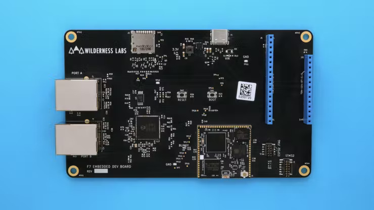
The Meadow F7 Core-Compute System on Module has 64MB of flash storage and 32MB of memory with an onboard Antenna and external µFl Antenna connector. Meanwhile, the Meadow F7v2 Core-Compute Dev Kit has two dual ethernet ports and an SD card slot for increasing the onboard storage. Both embedded devices are currently available for preorder with expected shipping on July 1, 2022. The Meadow F7 Core-Compute System on Module is priced at $45.00 and the Meadow F7v2 Core-Compute Dev Kit can be bought for $100.00 with a limit of 25 and 5 per customer respectively.
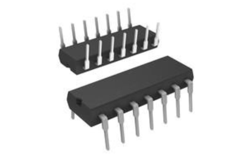
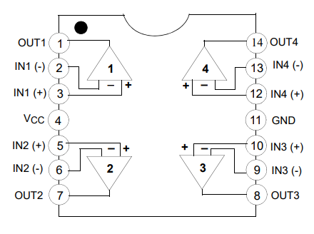
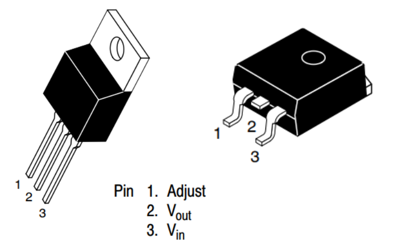
A Hong Kong and Canada-based components distributor that provides domestic support services, Utmel Electronics has announced the availability of a linear operational amplifier and a voltage regulator for embedded applications across various industries. The linear operational amplifier LM324N, manufactured by ON Semiconductor, consists of four high gains, internally frequency compensated operational amplifiers designed to operate on a single power source over a wide range of voltages. While the voltage regulator LM317T, also manufactured by ON Semiconductor, is an adjustable 3-terminal positive voltage regulator capable of supplying excess 1.5A over an output voltage range of 1.2V to 37V.
What is an operational amplifier?
Operational amplifiers, also commonly referred to as op-amps, are basic building blocks for analog circuits. We typically find them in radio transceivers, and Analog Devices, being one of the top manufacturers of radio devices, you can find Op-amps in many of the schematics. Irrespective of the manufacturer, operational amplifiers are widely used embedded devices for ideal DC amplification and are adopted for signal filtering. An operational amplifier has three terminals consisting of two high impedance inputs out of which one of the inputs is called the inverting input (also marked with a negative sign) and the other input is the non-inverting input (marked with a positive sign). The third terminal is the output port that can sink and source voltage or current.
The LM324N quad operational amplifier features a large DC voltage gain of around 100 dB, and a wide power supply range of 3V to 32V depending on the version– LM324/LM324A. Some of the other features are that the input common-mode voltage range includes ground, and the large output voltage swing ranges from 0V to Vcc-1.5. The company provides more details on the application areas for the operation amplifier, and those include transducer amplifiers, DC gain blocks, and all the conventional operational amplifier circuits that can be easily implemented in a single power supply system.
Since LM324N is a linear operational amplifier, the output signal is the amplifier factor, also known as amplifier gain multiplied by the value of the input signal. Because most of the analog circuits today demand voltage amplifiers, LM324N is a linear voltage amplifier with Vin and Vout as the input and output signals.
What is a voltage regulator?
The voltage regulator is part of a power supply unit that ensures a steady voltage supply across all operating conditions. The device is primarily used for regular voltages during power fluctuations and variations in the load. Voltage regulators are commonly classified as linear and switching regulators. Linear regulators use internal circuitry and use a differential amplifier to control output voltage against the reference voltage while switching regulators toggle a series of devices on and off at high frequency. However, the LM317T voltage regulator falls under the category of DC linear adjustable voltage that allows modifying the output voltage based on the two resistors.
The LM317T adjustable output voltage regulator is a 3-terminal device and is claimed to be “b” with only two external resistors to set the output voltage. The 3-terminals are adjustment, Vout, and Vin with a heatsink surface connected to pin 2 (Vout). The LM317T voltage regulator employs an internal current limiting circuit, thermal shutdown, and safe area compensation for making it “blow-out proof.” Current limiting is included to limit the peak output current to a safe value, while a thermal shutdown is provided to keep the IC from overheating. If the internal dissipation increases, the regulator will shut down to prevent excessive heating.
The LM317T voltage regulator serves a wide range of applications including local, on-card regulation. For it to behave as a precision current regulator, the developer can make a programmable output regulator by connecting a fixed resistor between the adjustment and output.
Conclusion
Linear operational amplifiers, LM324, are widely used in analog and power applications such as voltage buffers, analog filters, and threshold detections, among many others. Voltage regulators, LM317T, are one of the important components of any electronic circuit that uses a power supply unit of any scale. As they take care of the voltage regulator for fluctuations, they keep the internal circuitry safe. Utmel Electronics has not provided pricing for the LM324N linear operational amplifier, but interested people can request a quote with the quantity required. The same applies to LM317T for which you can request a quote.
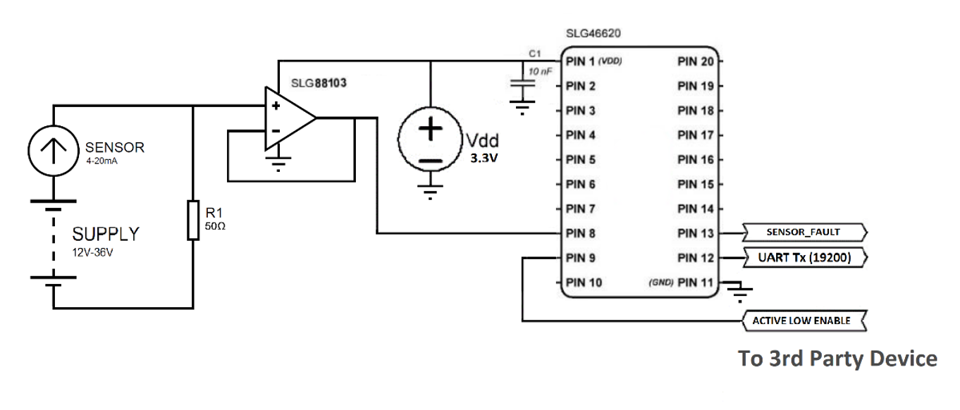
Current loop output sensors are used to transmit data over long distances without dropping the sensor output value. Signal conditioning is performed at the receiving end to analyze and measure the output value. Generally, the output signal is in the range of 4 – 20mA before being conditioned and processed.
This article describes how to use GreenPAK™ for signal conditioning of current loop output sensors. To confirm the sensors are working properly, the GreenPAK design outputs a digital LOW signal when the sensor is disconnected from the system.
This GreenPAK design has an input range of 4 – 20mA and outputs the serial data over the UART Tx line at a 19200 baud rate. The signal can then easily be read on any third-party device on the UART Rx pin.
The SLG88103 IC is used as a front-end operational amplifier to convert the current loop signal to analog voltages from 0 – 1V. Next, a SLG46620 is used to convert this analog signal to the RS232 protocol. The SLG46620V is a low-power, cost-effective, small device that can substitute for a system of discrete ICs and passive devices. This unique blend makes the SLG46620 an ideal candidate for portable, cost-sensitive consumer products.
1. Design Overview
Current loop sensors are usually powered through a 12 – 36VDC power source. In this design, the sensor is supplied with a constant DC voltage source in series with a 50Ω resistor. The output current ranges from 4 – 20mA.
We know that by Ohm’s Law, V=IR. At 4mA of current through the 50Ω resistor, the voltage is 0.2V. This is the minimum voltage of the sensor output. At 20mA of current through the 50Ω resistor, the voltage is 1V. This is the maximum voltage of the sensor output.
Whenever the sensor is disconnected from the system, the current through the resistor drops to 0mA and the voltage drops to 0V. We can sense this dropped voltage to detect if the sensor is connected to the system or not.
After conversion, the output from the op amp is fed directly to the SLG46620V at PIN8. Using PGA, ADC, DFFs, and LUTs, the signal through PIN8 is converted to the RS232 protocol, at a configuration of 8 data bits, with 1 even Parity bit at 19200bps. The IC then outputs the data serially on PIN12. To check if the sensor is connected to the system or not, the IC outputs a digital LOW signal at PIN13 whenever the sensor is disconnected from the system.
To make the circuit power efficient, an enable pin (PIN9) disables all the SLG46620V’s macrocells when pulled HIGH, reducing the total power consumption of the IC to less than 10µA. This feature not only decreases the overall current consumption of the system, but also gives control to the third-party device to decide when to process data.
The internal working of the SLG46620V’s macrocells is discussed in detail in the GreenPAK Design section.
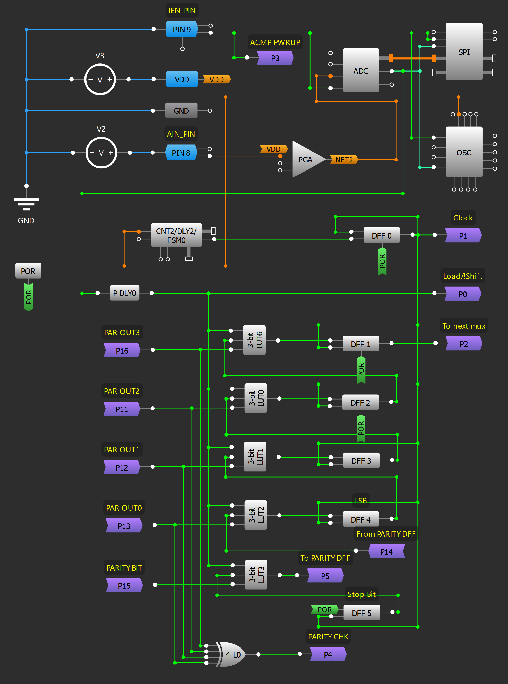
Figure 1: System Schematic
2. GreenPAK Design
The design consists of three parts:
Analog to parallel data conversion
Parallel to serial data conversion
Adding Start, Parity and Stop bits
The complete design file can be found here. It was created in free GUI-based GreenPAK Designer software – a part of Go Configure™ Software Hub.
2.1. Analog to Parallel Data Conversion
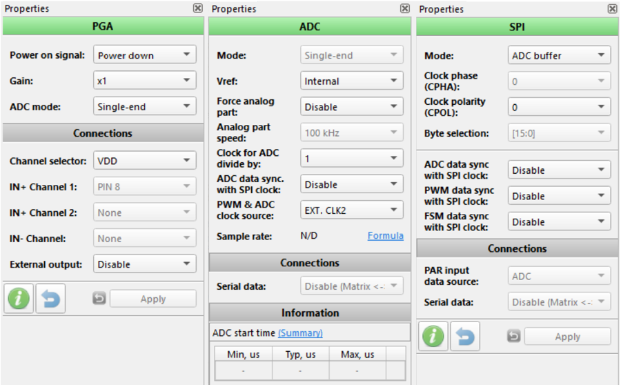
The IC receives the external analog signal through PIN8, which is configured to operate as an analog input/output. The signal then passes through a Programmable Gain Amplifier, or PGA, which sets the gain. Then, the signal enters the analog-to-digital converter (ADC) block. The operation mode of the ADC is single-ended with x1 gain.
The ADC macrocell converts the analog signal in 8 bits of corresponding digital data. This 8-bit digital data from the ADC is fed directly to the SPI macrocell. The configuration of the PGA, ADC, and SPI macrocells can be seen in Figure 2. The SPI macrocell allows parallel data output. By enabling the block in Matrix 1, we can have the data on 8 parallel bits.
Figure 2: PGA, ADC, and SPI Configuration
The PWM and ADC clock source is defined as EXT. CLK2, which is the frequency at which our data will be outputted serially from the GreenPAK (19200 bits per second).
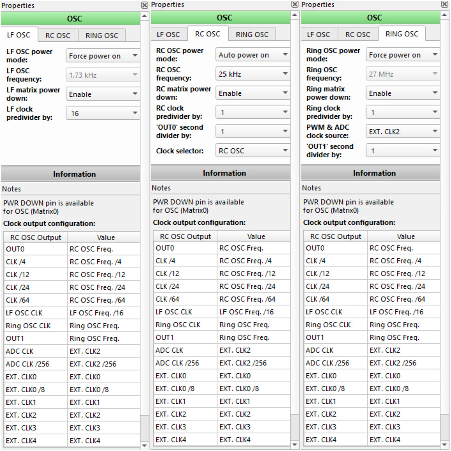
The configuration of the OSC macrocell is shown in Figure 3.
Figure 3: OSC Configuration
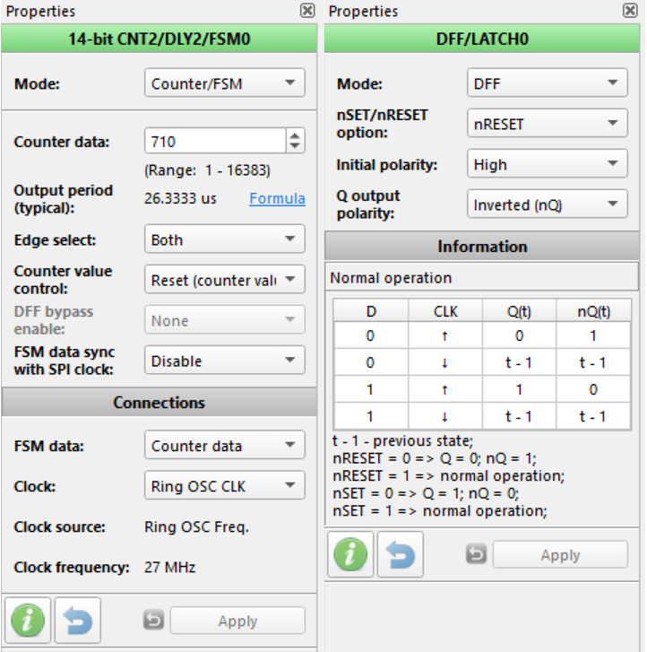
We have generated a clock frequency of 19.2kHz using the 14-bit CNT2/DLY2 and DFF0. This 19.2kHz frequency signal is not only used as the clock source of the ADC, but also to convert parallel data from the parallel data output block to serial data. This is explained further in the next section.
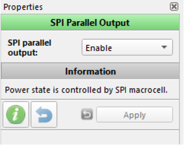
SPI Parallel Output configuration (in Matrix1) is shown in Figure 4.
Figure 4: SPI Parallel Output Configuration
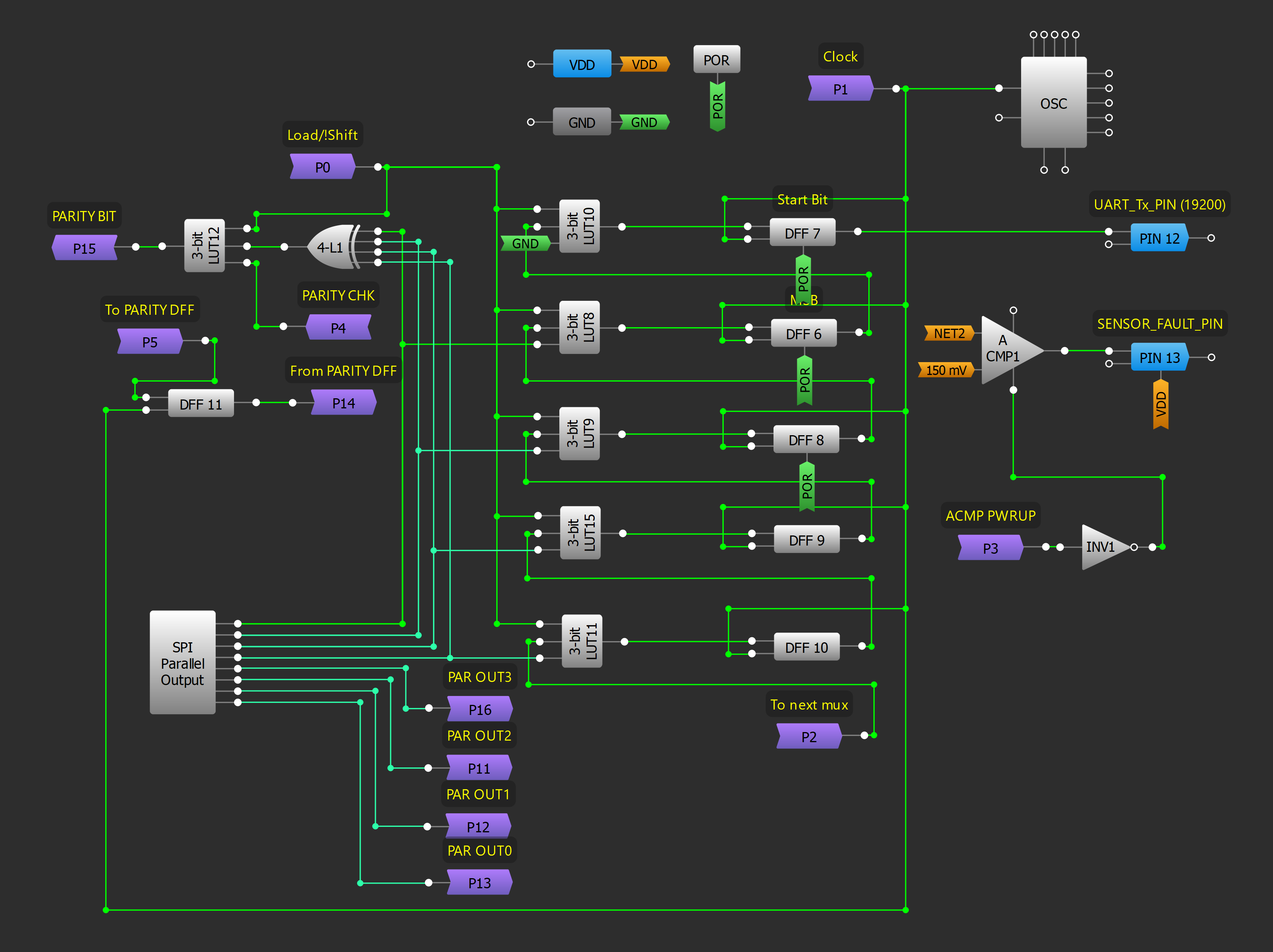
In the below figure, some wires from Matrix0 are connected to those in Matrix1. GreenPAK Designer has ports to carry signals between matrices. Out-ports from one matrix are available in the other matrix as In-ports, and vice versa.
Figure 5: Matrix0
2.2 Parallel to Serial Conversion
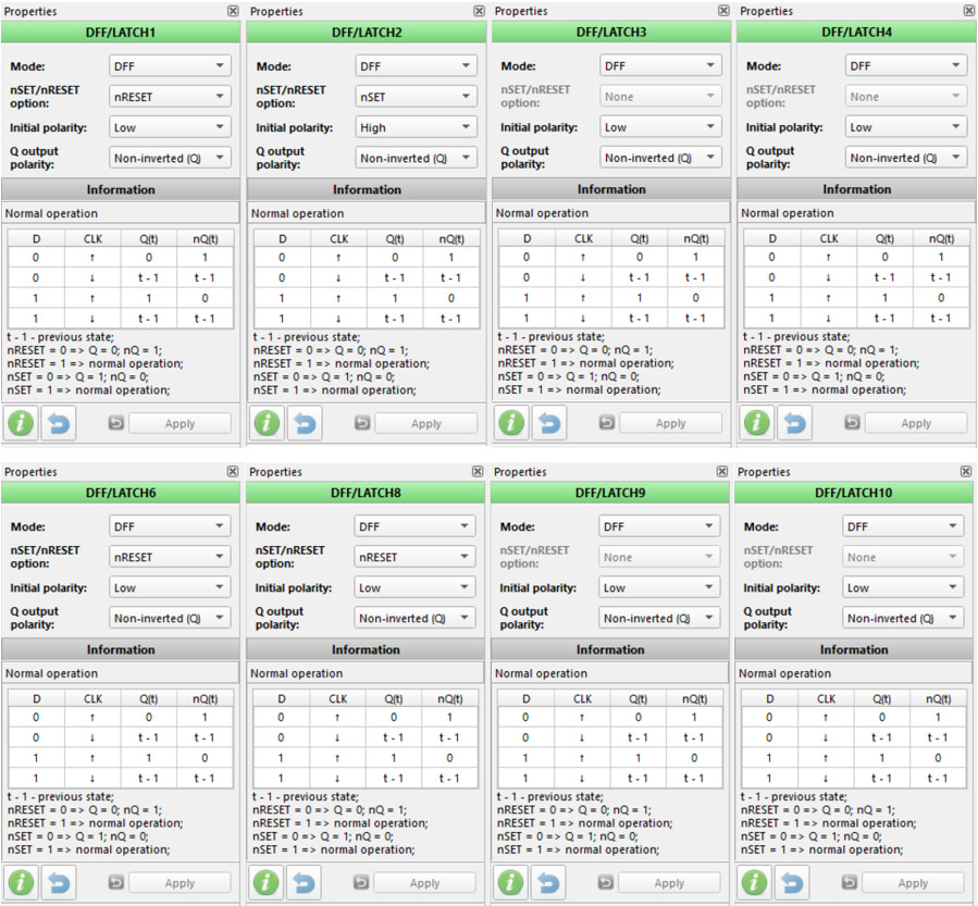
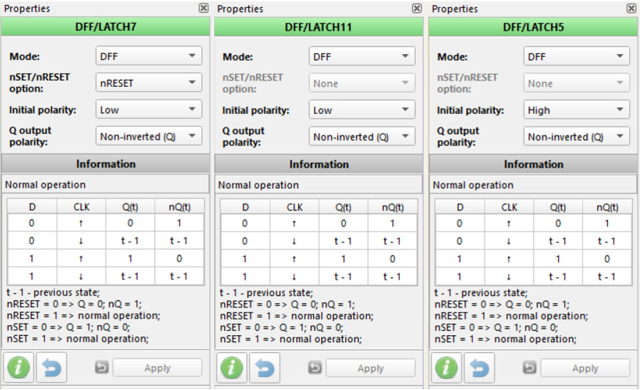
The data from the Parallel Data Output macrocell in Matrix 1 is converted to serial data using a Parallel-In-Serial-Out (PISO) shift register. DFF1, DFF2, DFF3, DFF4 in Matrix0 and DFF6, DFF8, DFF9, DFF10 in Matrix1 are used as 8-bit PISO shift registers to store and transmit data from SPI parallel output serially to PIN12. DFF7, DFF11 and DFF5 are used to add Start, Parity and Stop bits respectively to the serial data. We will discuss these in the next section. Figure 6 shows the configuration of the 8-bit PISO DFFs.
Figure 6: PISO DFF Configuration
The 8 parallel output bits from the SPI parallel output block are connected with the 8-bit PISO DFFs at the D pin of each DFF. A clock is applied at the CLK pin of the DFFs, which controls the shifting of the bits in the DFFs. Every time a rising edge is inputted at the CLK pin of a DFF, the value (0 or 1) stored in that DFF is shifted to the next DFF. In this way, after 8 consecutive high pulses at the CLK pins, the 8-bit data is outputted from the PISO shift register.
The clock signal at the input of the DFFs is generated using the 14-bit CNT2/DLY2 and DFF0. The frequency of this clock signal is 19200Hz. At this frequency, the GreenPAK communicates at a common baud rate of the RS232 protocol. The most common baud rates are 4800, 9600, 19200, 38400, 57600, and 115200. By selecting the 19200Hz frequency, the data transmit at 19200bps serially through the PISO shift register. The configuration of the 14-bit CNT2/DLY2 and DFF0 are shown in Figure 7.
Figure 7: 19200Hz Frequency Generator
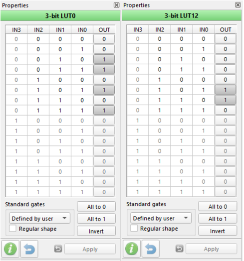
After every successful transmission of the 8-bit data, the next step is to load the next 8 bits of data into the shift register. To do this, we use 3-bit LUTs to form a multiplexer (MUX) design within the SIPO. LUT0, LUT1, LUT2, LUT3, and LUT6 in Matrix0, and LUT8, LUT9, LUT10, LUT11, LUT12, and LUT15 in Matrix1 are used as MUXs.
All these LUTs have exactly the same configuration, except LUT12. Figure 8 shows the configuration of the LUTs.
Figure 8: LUT Configuration
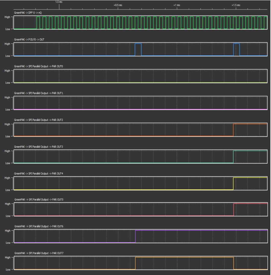
To load the data within the DFFs, we’ll first look at the timing diagram of the ADC and SPI parallel outputs with respect to the 19200Hz clock frequency as shown in Figure 9.
Figure 9: 8-bit Parallel Data Timing Diagram
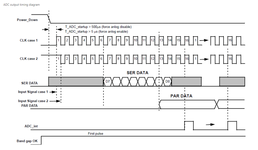
The first waveform in green is the 19200Hz clock signal. The ADC is also supplied with this clock frequency through EXT. CLK2 of the OSC block. The next waveform is the ADC_INT signal of the ADC macrocell. According to GreenPAK Designer, “The Interrupt output is one clock period long and signifies the PAR data is valid.” See the timing diagram of the ADC output in Figure 10.
Figure 10: ADC Output Timing Diagram
Using the INT signal from the ADC_INT pin, we will be notified that the data at the parallel bits of the parallel data output is ready to be loaded in the DFFs.
Have a look at the next 8 waveforms carefully. Notice that the states of the outputs are changing with every rising edge of the INT signal. The first signal is PAR OUT0, and it is the least significant bit. The last signal is PAR OUT7, and it is the most significant bit.
By using the multiplexers, we can check for the INT rising edge and load the data into the 8-bit PISO DFFs. The time duration between two consecutive INT pulses is the time we will use to transmit the data serially from the GreenPAK.
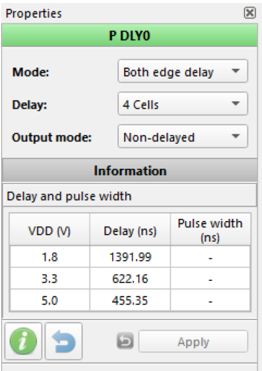
Figure 11: Programmable Delay
A Programmable Delay (P DLY) logic cell is used to generate a small delay in the signal. We have used this to generate an approximately 500ns delay at the interrupt signal of the ADC to make sure that the data at the parallel output block is available.
Figure 12: Matrix1
2.3 Adding Start, Parity, and Stop Bits
The RS232 protocol communicates 8 data bits in a single packet, with 1 Start bit, 1 Parity bit, and 1 or more Stop bits. After the conversion of our data from an analog signal to parallel data and then to serial data, the last step is to add these bits so that our data becomes standard RS232 data.
DFF7 is used to load the Start bit. The Start bit is one clock pulse long, a digital LOW signal which indicates the start of the data. The next 8 bits after the Start bit are the 8 bits of data.
After the transmission of the Start and 8 data bits, the next bit is a Parity bit. This is either HIGH or LOW depending on the number of 1s in the 8 bits of data. We have a LOW Parity bit if the number of 1s is even and a HIGH Parity bit if the number of 1s is odd. For example, if we have our 8 data bits as 01101000, we have an odd number of 1s and the Parity bit must be HIGH.
To generate a Parity bit, we have used the 4-bit LUT0 in Matrix0, and the 4-bit LUT1 in Matrix1 as XOR gates. An XOR gate has an output HIGH if the number of 1s on the input is odd, and an output LOW if the number of 1s is even. We have inputted these LUTs with the 8 parallel output bits from the SPI parallel output macrocell. At the rising edge of the interrupt signal from the ADC, we check the number of 1s and load the parity bit into DFF11.
A Stop bit is one or more HIGH bits sent after successfully transmitting 1 Start bit, 8 data bits, and 1 Parity bit serially. DFF5 is used to load the Stop bit.
Figure 13 shows the configuration of DFF7, DFF11, and DFF5 for the Start, Parity and Stop bits respectively.
Figure 13: Start, Parity, and Stop bit Configuration
2.4 Sensor Fault Detection
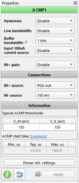
Another interesting feature we can generate using GreenPAK is sensor fault indication. We have used an analog comparator for this purpose, which outputs a digital LOW signal at PIN13 of the GreenPAK SLG46620V whenever the voltage at the input drops below 150mV.
The current loop sensors have a minimum output value of 4mA and a maximum of 20mA. But whenever the sensor is disconnected from the loop, the current drops to 0mA. This results in a signal of 0mV at the AIN_PIN (PIN8 of SLG46620). This signal is fed directly to the third-party device (e.g., Arduino).
ACMP1 in Matrix1 is used as the sensor fault detector. IN+ is set to 150mV, while IN- is supplied with a NET connection from the PGA macrocell.
To enable this feature, we apply the active low enable signal into the inverter INV1 in Matrix1 and connect the output of INV1 to the PWR UP pin of the ACMP1. Figure 14 shows the configuration of ACMP1.
Figure 14: ACMP1 Configuration
3. Results
The Signal Wizard included in GreenPAK Designer lets us examine the design and ensure it works as expected.
Signal Wizard is very convenient for design inspection, where signals of different shapes can be generated without the need to use an external signal generator. The signal frequency and amplitude can be easily controlled. A custom signal can also be generated.
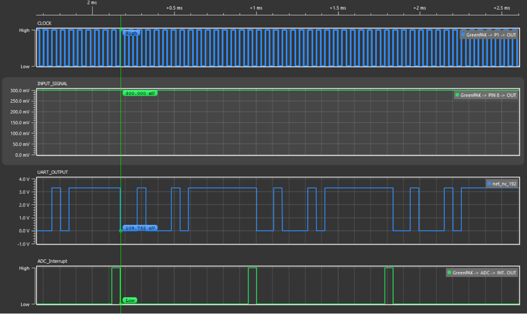
The test results are shown in Figure 15. The second waveform is the input signal applied to the AIN_PIN. Consider the signal at 2.2ms in the signal wizard. It is 300mV. At this position, with the rising edge of the clock signal (last waveform), the UART data is available at PIN12 (third waveform).
Every UART bit starts at the rising edge of the clock signal. The first bit is a LOW signal (0). This indicates the Start bit. The next 8 bits are decoded as 01000101. These are the 8 data bits which carry the actual data.
The bit after the 8 data bits is the Parity bit, which shows the number of 1s in the data. We have a HIGH signal (1) as the Parity bit because the number of 1s are odd in this case.
After the Parity bit, the next 1 or more bits are HIGH Stop bits.
The next data packet starts at the falling edge of UART.
Figure 15: Results
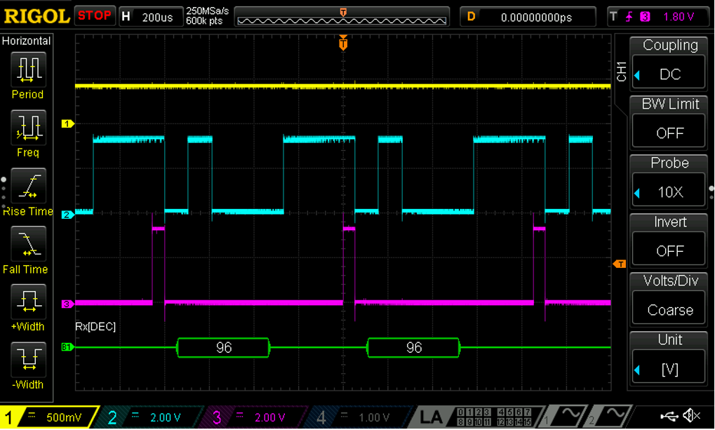
Consider the next UART falling edge at approximately 2.2ms + 0.8ms. The first bit (0) is again a Start bit, followed by the same data bits 01000101, and a Parity bit of 1 since the number of 1s is odd.
Figure 16: Waveform on Oscilloscope
4. Arduino Code
Following is the bare minimum code for reading values from GreenPAK on an Arduino development board.
#include <SoftwareSerialParity.h>
SoftwareSerialParity GreenPAK(2, 3); // RX, TX
int i;
void setup()
{
  GreenPAK.begin(19200,EVEN);
  Serial.begin(19200); // start serial to PC
}
void loop()
{
  if (GreenPAK.available() > 0)
  {
  i = GreenPAK.read();
  Serial.print(i, DEC);
  Serial.print(" ");
  }
}
The “Software Serial Parity” library is used to read data with even parity through Arduino. See the References section for more information.
Conclusion
This article outlines how to build a signal conditioning circuit using a GreenPAK, which includes a current loop to RS232 converter circuit at a 19200 baud rate.
The GreenPAK IC demonstrates a high efficiency for integrating several functions in a low-cost and small-area IC solution, making it especially suitable for industrial devices.
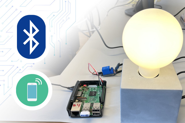
Home automation involves automating household environment equipment. To achieve that, we have created a smart bulb that can be controlled remotely using a smartphone app. The aim of this project is to control different home appliances using smartphones at your home.
Introduction
This example is showing how to control a GPIO pin on a RaspberryPi remotely from a smartphone (or another BleuIO Dongle).
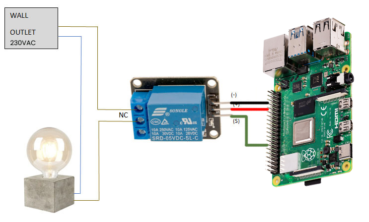
A way to connect to the GPIO Pin (Like a 5V Relay and a Lightbulb)
WARNING – THIS PROJECT INVOLVES HIGH VOLTAGES THAT CAN CAUSE SERIOUS INJURY OR DEATH. PLEASE TAKE ALL NECESSARY PRECAUTIONS, AND TURN OFF ALL POWER TO A CIRCUIT BEFORE WORKING ON IT.
Beware:
Always be very careful when experimenting with AC, electrical shock can result in serious injuries! NOTICE OF RISK; DISCLAIMER OF LIABILITY
WARNING – THIS PROJECT INVOLVES HIGH VOLTAGES THAT CAN CAUSE SERIOUS INJURY OR DEATH. PLEASE TAKE ALL NECESSARY PRECAUTIONS, AND TURN OFF ALL POWER TO A CIRCUIT BEFORE WORKING ON IT.
Connecting the relay
Always be very careful when experimenting with AC, electrical shock can result in serious injuries! NOTICE OF RISK; DISCLAIMER OF LIABILITY
Instructions for bleuio_rpi_switch_example.py
Connect the BleuIO Dongle to your RaspberryPi.
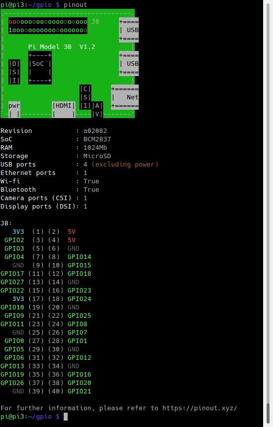
Edit the variable ‘switch’ in the script to the GPIO pin you want to use. (You can use the command pinout to get a graphical view showing you the GPIO pins for the board)
Finally, just run the python script and use your phone to connect to the BleuIO Dongle and send on/off messages to control the GPIO!
Instructions for connecting to the BleuIO to mobile
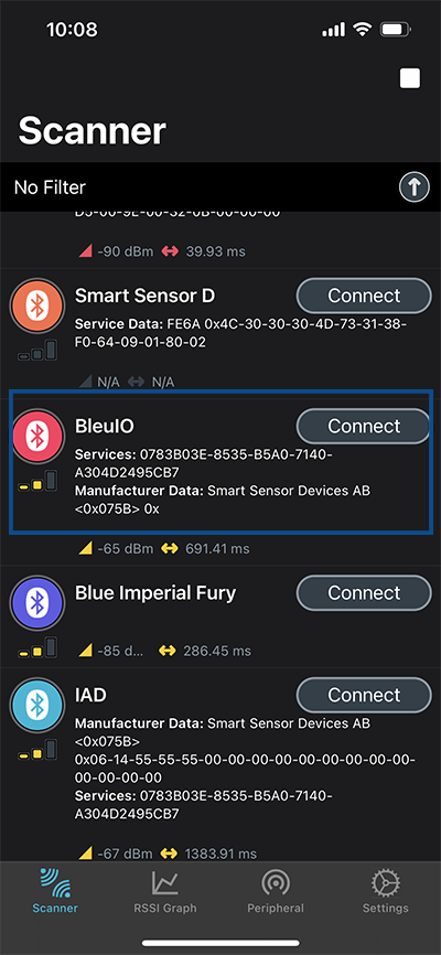
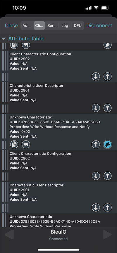
Download a BLE scanning App that can connect and read/write to a device. (Like nRFConnect or BLEScanner) Android, IOS
Look for the dongle, it will be advertising as ‘BleuIO’.
Connect to the BleuIO Dongle.
To enable BleuIO to recieve commands you must first write 0x01 to the Flow Control characteristic (UUID: 0783b03e-8535-b5a0-7140-a304d2495cb9)
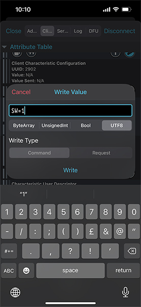
Now you can write to the Server RX Data characteristic (UUID: 0783b03e-8535-b5a0-7140-a304d2495cba) to control the GPIO.“SW=1” for ON “SW=0” for OFF
The script
Here is the python script that receives the messages from the smartphone app and helps control the light.
#!/usr/bin/python3
# Copyright 2022 Smart Sensor Devices in Sweden AB
#
# Permission is hereby granted, free of charge, to any person obtaining a copy of this software and associated documentation files (the "Software"),
# to deal in the Software without restriction, including without limitation the rights to use, copy, modify, merge, publish, distribute, sublicense,
# and/or sell copies of the Software, and to permit persons to whom the Software is furnished to do so, subject to the following conditions:
# The above copyright notice and this permission notice shall be included in all copies or substantial portions of the Software.
#
# THE SOFTWARE IS PROVIDED "AS IS", WITHOUT WARRANTY OF ANY KIND, EXPRESS OR IMPLIED, INCLUDING BUT NOT LIMITED TO THE WARRANTIES OF MERCHANTABILITY,
# FITNESS FOR A PARTICULAR PURPOSE AND NONINFRINGEMENT. IN NO EVENT SHALL THE AUTHORS OR COPYRIGHT HOLDERS BE LIABLE FOR ANY CLAIM, DAMAGES OR OTHER LIABILITY,
# WHETHER IN AN ACTION OF CONTRACT, TORT OR OTHERWISE, ARISING FROM, OUT OF OR IN CONNECTION WITH THE SOFTWARE OR THE USE OR OTHER DEALINGS IN THE SOFTWARE.

import time
import serial.tools.list_ports
import serial
import RPi.GPIO as io


switch = 7  # Edit this to suit your setup! (7 = GPIO 04), use command pinout to graphically show you the GPIO pins for the board
io.setmode(io.BOARD)
io.setup(switch, io.OUT)

master_array = []
index = 1
dongle_port = ""

print("\nWelcome to BleuIO RaspberryPi Switch Example!\n")

print("\nPlease insert dongle...")
try:
    while len(master_array) == 0:
        m_ports = serial.tools.list_ports.comports(include_links=False)
        for port in m_ports:
            if str(port.hwid).__contains__("VID:PID=2DCF"):
                master = port.device + " " + port.hwid
                if master.__contains__("VID:PID=2DCF:6002"):
                    print("Found dongle in port: %s" % port.device)
                    master_array.append(master)
                    dongle_port = port
                    break

    for dongle in master_array:
        print("\nConnecting to BleuIO @ %s\n" % dongle)

    time.sleep(0.5)
    dongle_conn = serial.Serial(
        dongle_port.device,
        115200,
        timeout=1,
    )

    if not dongle_conn.is_open:
        dongle_conn.open()

    print("Starting Advertising...")
    dongle_conn.write("AT+GAPDISCONNECTALL\rAT+DUAL\rAT+ADVSTART\rATI\r".encode())
    read_tries = 0
    dongle_resp = ""
    while read_tries < 20:
        dongle_resp = dongle_conn.readline().decode()
        if "Not Advertising" in dongle_resp:
            dongle_conn.write("AT+ADVSTART\r")
        if b"Advertising\r\n" in dongle_resp.encode():
            break
        read_tries += 1
        time.sleep(0.01)

    if dongle_resp:
        print("BleuIO is %s" % dongle_resp)
    else:
        print("ERROR! No response...")
        exit()

    print(
        "Going into loop, waiting for signal to turn switch on/off...\n(Press Ctrl+C to abort)"
    )
    while True:
        try:
            dongle_resp = dongle_conn.readline().decode()
            if "SW=0" in dongle_resp:
                print("Turn Switch off!")
                io.output(switch, io.LOW)
            if "SW=1" in dongle_resp:
                print("Turn Switch on!")
                io.output(switch, io.HIGH)
        except KeyboardInterrupt:
            if dongle_conn.is_open:
                dongle_conn.write("AT+GAPDISCONNECTALL\rAT+ADVSTOP\r".encode())
                dongle_conn.close()
                io.cleanup()
            print("\nBye!")
            exit()

except Exception as e:
    print("(ERROR: %s)" % (e))
Output
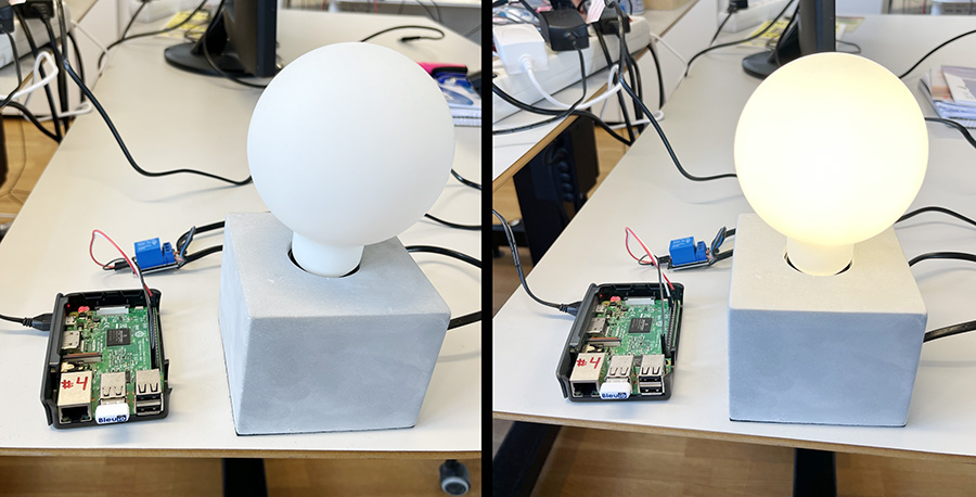
We have tested the script using nRFConnect app from both IOS and Android phones to turn on/off the light bulb. Here is the output of this project.
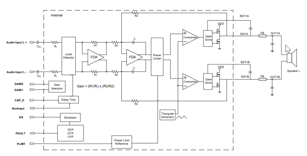
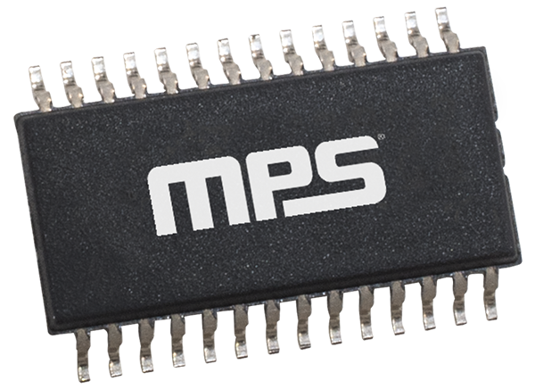
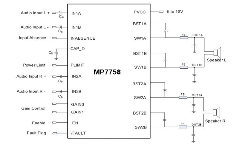
Monolithic Power SystemsMP7758 Audio Amplifiers are inductor less, fixed frequency, analog input Class-D audio amplifiers that drives power stereo speakers in a bridge-tied load configuration. These amplifiers are completely integrated thus reducing the solution size. The MP7758 audio amplifiers integrate 240mΩ power MOSFETs and short-circuit protection circuits. These audio amplifiers feature start-up/shutdown pop elimination, advanced EMI performance and are capable of passing EMC tests without an inductor. The MP7758 audio amplifiers are capable of delivering 15W per channel into 8Ω speakers with a 16V power supply utilizing a stereo BTL structure. These devices exhibit a high fidelity of class-AB amplifiers, with high efficiency, offer an adjustable power limit (PLIMIT) function, and fault output flag. The MP7758 audio amplifiers are widely used in wireless/portable speakers, TVs, DVD receivers, and active speakers.
Features
5V to 18V operation from a single supply
±5A peak current output
Output power:
9.5W/channel at 12V, 8Ω load, 10% THD, 15W/channel at 16V, 8Ω load, 10% THD
90% efficiency with 8Ω load, 10% THD, 1kHz, 12V supply voltage
240mΩ power MOSFETs
Start-Up/Shutdown pop elimination
Short-circuit protection circuits
Inductorless topology
Advanced EMI performance
All switches are current limited
Internal Under-Voltage Protection (UVP)
Internal thermal protection
Adjustable power limit
Automatic shutdown with zero input signal detection
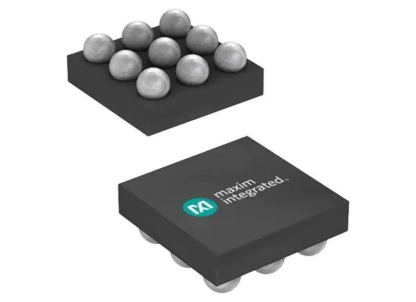
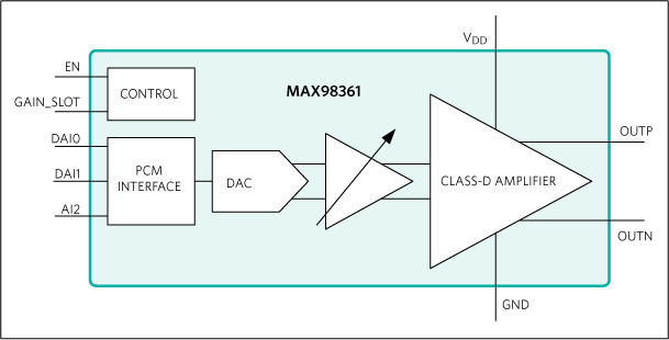
Maxim Integrated MAX98361 Plug-and-Play Digital Class-D Amplifiers are easy-to-use, low-cost, digital pulse-code modulation (PCM) input amplifiers featuring industry-leading, Class-AB audio performance with Class-D efficiency. The MAX98361 has a digital audio interface that automatically recognizes different PCM and TDM clocking schemes, eliminating the need for I2C programming. This easy-to-use amp allows users to supply power, LRCLK, BCLK, and digital audio to generate audio. Additionally, a novel pinout enables users to use the cost-effective WLP package without expensive vias.
The Maxim MAX98361 Plug-and-Play Digital Class-D Amplifiers provide a flexible digital audio interface, supporting I2S, left-justified, and 8-channel time division multiplexed (TDM) data formats. The digital audio interface accepts 8kHz, 16kHz, 32kHz, 44.1kHz, 48kHz, 88.2kHz, and 96kHz sample rates. Meanwhile, data words can be 16-bit, 24-bit, or 32-bit in I2S and left-justified modes and 16-bit or 32-bit in TDM mode. The device’s digital audio interface input thresholds are ideal for interfacing to 1.2V and 1.8V logic, with the device tolerating logic input voltages up to 5.5V.
The MAX98361A and MAX98361B offer fast 1ms turn-on times, while the MAX98361C and MAX98361D ramp the volume over 13ms during turn-on and turn-off. The amps eliminate the need for the external MCLK signal typically used for PCM communication. These features reduce EMI and possible board coupling issues and reduce the size and pin count.
The MAX98361 is specified over the -40°C to +85°C temperature range.
Features
Simple plug-and-play design
Single-supply operation (2.5V to 5.5V)
3.2W Output power into 4Ω at 5V
2.2mA Quiescent current
1ms Turn-on time (for MAX98361A and MAX98361B)
92% Efficiency (RL = 8Ω, THD+N = 10%)
10μVRMS Output noise
110dB Dynamic range
Low 0.009% THD+N at 1kHz
No MCLK Required
Sample rates of 8kHz to 96kHz
Supports left, right, or (left/2 + right/2) output in I2S and left-justified modes
Sophisticated edge rate control enables filterless class-D outputs
81dB PSRR at 217Hz
1.5μA Standby current allows elimination of GPIO for EN pin
Low RF susceptibility rejects TDMA noise from GSM radios
Class-D Switching frequency trimmed to 5% for better EMI planning
Extensive click-and-pop reduction circuitry
Robust short-circuit and thermal protection
Available in space-saving package 9-Pin WLP (0.4mm pitch)
3.69mm2 Solution size for WLP with a single bypass capacitor
Designed for consumer electronics applications, including tablets, robotic appliances, and power tools.
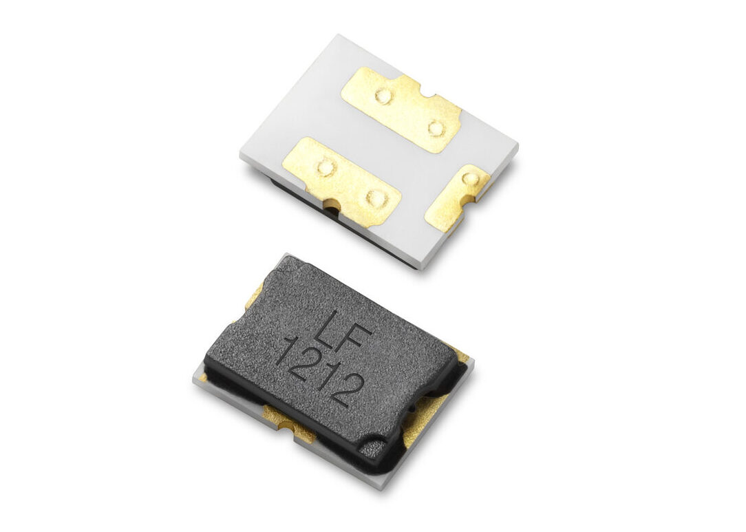
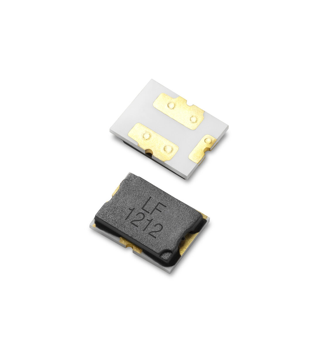
Littelfuse, Inc., an industrial technology manufacturing company empowering a sustainable, connected, and safer world, announced the new ITV4030, a series of 22 amp, three-terminal, surface-mountable Li-ion battery protectors.
These 4.0 x 3.0 mm devices protect battery packs against overcurrent and overcharging (overvoltage) conditions. The innovative design uses embedded fuse and heater elements that provide fast response and reliable performance to interrupt the charging or discharging circuit before the battery pack becomes overcharged or overheated.
The ITV4030 Battery Protector is ideal for use in a wide range of data communications interfaces for consumer electronics, including:
Tablets
Power tools
Robotic appliances
E-bikes and e-scooters
Emergency radios and eCall
“The ITV4030 is a 22-amp rated device, which extends our ITV line of li-ion battery protectors to provide more options for electronics designers,” said Stephen Li, Global Product Manager at Littelfuse. “Expanding our portfolio of three-terminal surface-mountable battery pack protectors enables us to provide these innovative solutions to a broader range of applications.”
The ITV4030 offers these key benefits:
Surface mountable design simplifies automated PC board assembly processes.
Certifications from UL and TUV aid in securing approvals with meeting industry compliance requirements.
The environmentally friendly component is halogen-free and RoHS compliant.
How it works
An embedded three-terminal fuse cuts off the circuit when overcurrent issues occur. A heater element, directly embedded under the fuse element, generates enough heat to blow the fuse once overcharging is detected by IC or FET.
Availability
The ITV4030 is available in tape and reel format in quantities of 5,000. Place ample requests through authorized Littelfuse distributors worldwide. For a listing of Littelfuse distributors, please visit Littelfuse.com.
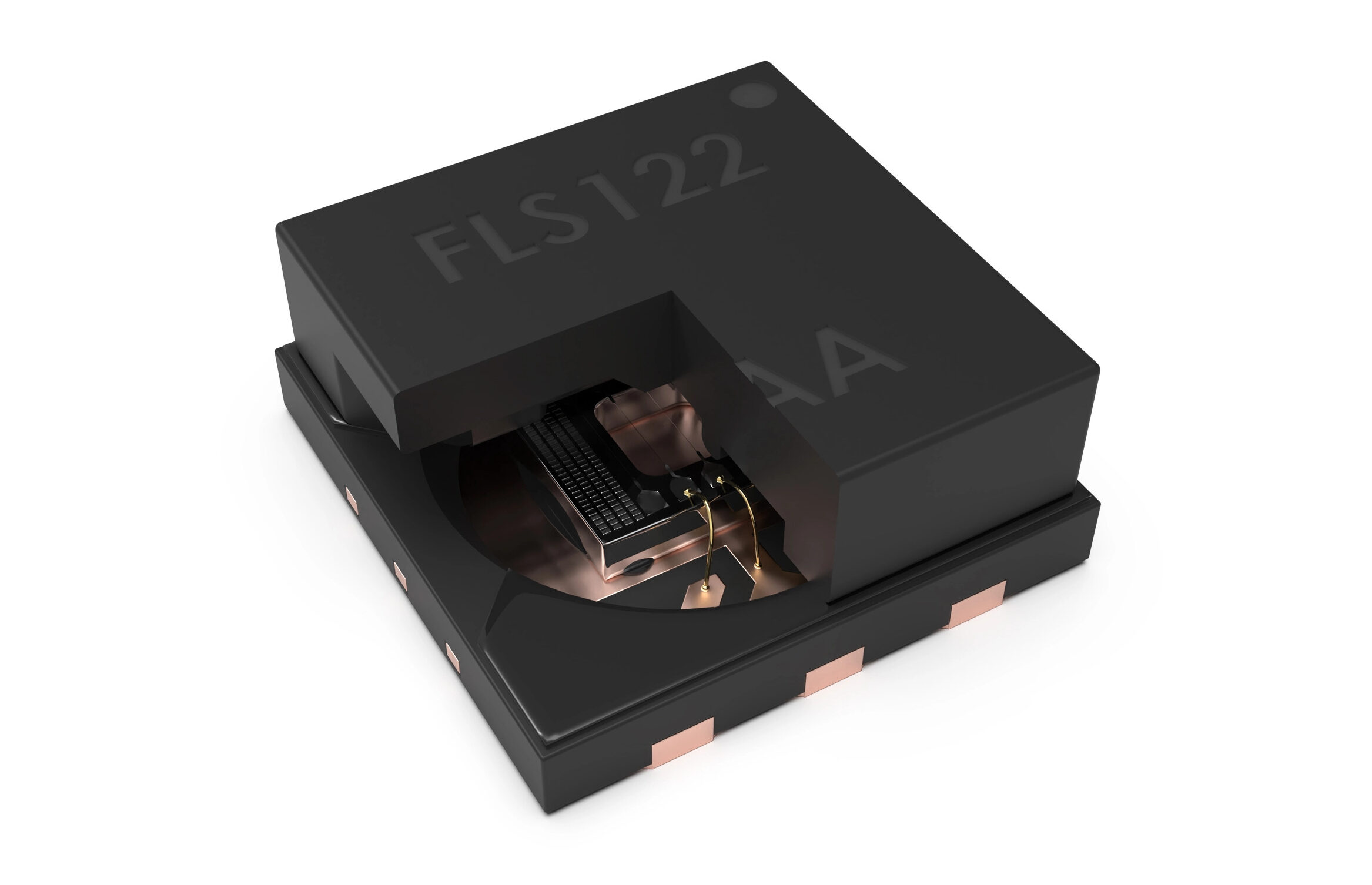
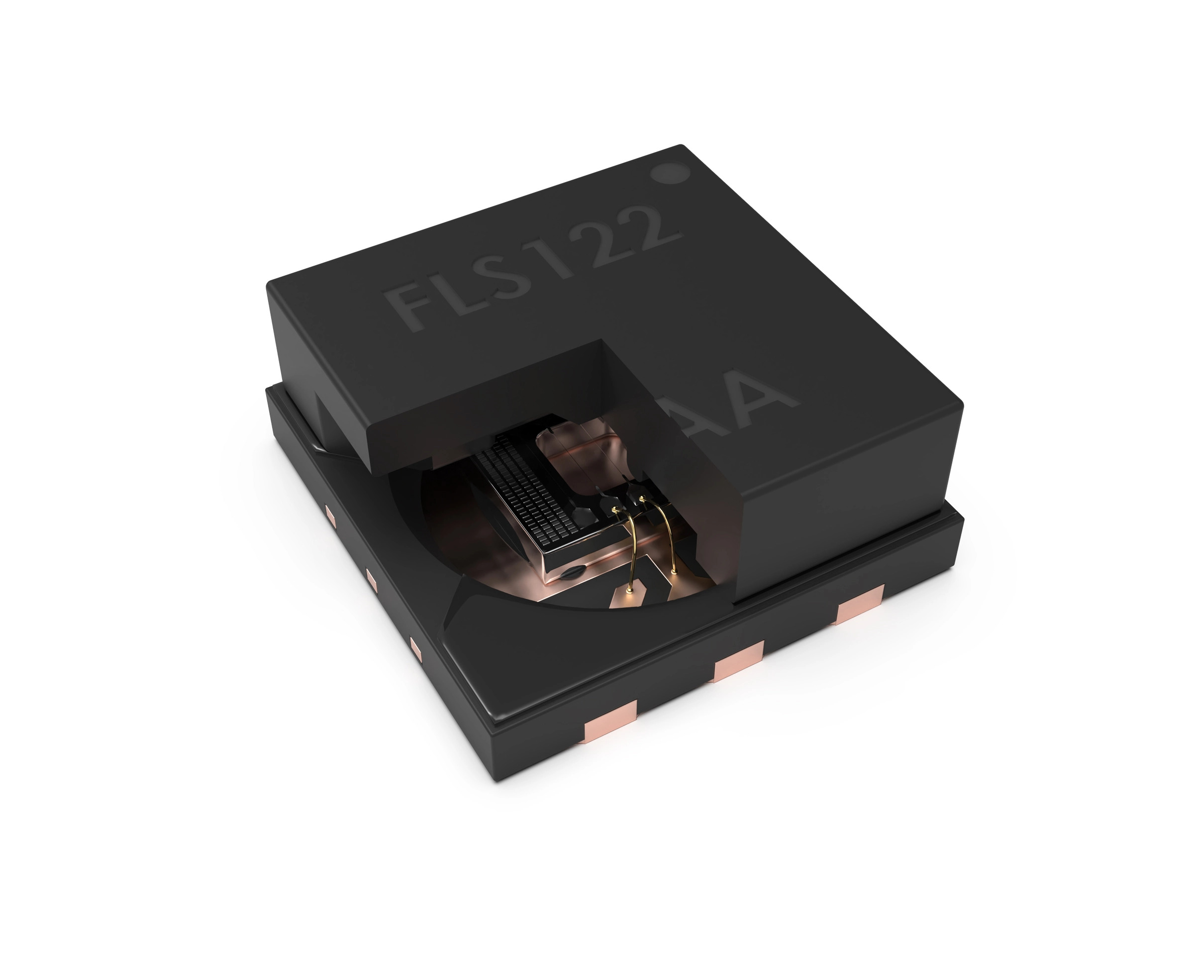
Flusso claims the FLS122 is the industry’s smallest air velocity sensor, measuring 3.5 × 3.5 mm, targeting space-constrained applications.
Flusso Ltd. has claimed the industry’s smallest air velocity sensor with the introduction of the FLS122, housed in a 3.5 × 3.5-mm footprint. This makes it 80% smaller than competitive devices, said the company.
Joining the FLS110 flow sensor, also housed in a 3.5 × 3.5-mm package, the FLS122 uses a CMOS die derived from the FLS110 and uses the same “novel” integration concept that allows manufacturers to decide how and where to integrate it, said the company. It also helps designers balance system performance versus cost depending on their requirements.
The FLS122 is designed for board-mounted air velocity measurements for thermal management and filter monitoring in space-constrained and challenging environments. It can be used in a variety of applications, including high-volume industrial, medical, and consumer markets. Target use cases include data centers and gaming PCs that require efficient air cooling to maximize performance and energy efficiency, and consumer appliances such as HVAC, air purifiers, and vacuum cleaners, said Flusso.
The FLS122 supports bidirectional flow sensing and can provide real-time temperature and airspeed measurement of up to 20 meters per second. It is integrated into a 6-pin DFN package with a specially-designed ‘tunnel lid’, which is optimized for accurate measurement of flow velocity with little or no pressure drop required in the flow path, according to the company.
Samples of the FLS122 are available to qualified customers on request. The sensor will be supplied with support material including an evaluation kit, hardware design guides, sensor firmware, and a software development kit, as well as application engineering support.
Flusso will showcase the new sensor for the first time at next week’s Sensor + Test 2022 event in Germany, May 10-12, in stand 1-331/1. The FLS122 also will be showcased at Sensors Converge in San Jose, California, June 27-29, in booth #1024.
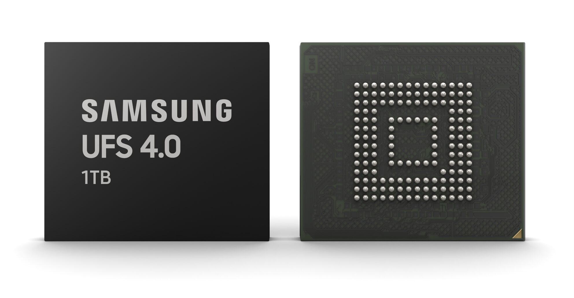
Samsung will be mass producing its UFS 4.0 in Q3 in a variety of capacities up to 1TB.
Samsung UFS 4.0 will provide speed of up to 23.2 Gbps per lane. That’s double the previous leading UFS solution (UFS 3.1).
This will make UFS 4.0 suitable for 5G smartphones with features requiring large amounts of data processing such as high-resolution images and high-capacity mobile game-playing, as well as for automotive and AR/VR applications.
With Samsung’s 7th-generation V-NAND and a proprietary controller, the newly developed Samsung UFS 4.0 will feature a sequential read speed of 4,200 megabytes per second (MB/s) and a sequential write speed of 2,800 MB/s, which will deliver approximately 2x and 1.6x faster speeds over the previous UFS 3.1 product, respectively.
sammobile.com writes:
UFS 4.0 storage will come in capacities of up to 1TB, which makes it the perfect fit for flagship Samsung Galaxy smartphones that come in multiple storage configurations. Again, it’s likely we’ll see UFS 4.0 being used in either Samsung’s next foldables or the Galaxy S23 series; Samsung will also be working with other manufacturers to make UFS 4.0 available in automotive, augmented reality (AR), and virtual reality (VR) applications and other Android smartphones.
Power efficiency has been enhanced. The devices will deliver a sequential read speed of up to 6.0 MB/s per milliampere (mA), representing a 46-percent improvement over UFS 3.1.
The memories will include an advanced Replay Protected Memory Block (RPMB). This design is 1.8 times more efficient in storing important personal data that can only be read or written through authenticated access.
The chips will have a maximum size of 11mm x 13mm x 1mm.