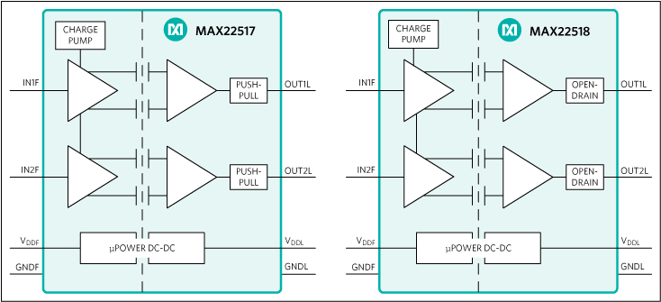
Maxim Integrated MAX22519 Digital Isolator is a dual-channel digital galvanic isolator with an integrated field-side supply. This digital isolator eliminates the bulky and expensive external isolated power supply when the power demand of the field side is small. The field-side power is supplied by the logic-side using an integrated isolated DC-DC converter. This digital isolator device is available with either push-pull or open-drain outputs and output default states are either logic-high or high impedance. The MAX22519 digital isolator features integrated isolated field-side supply, integrated galvanic digital isolation, integrated surge, and short protection with external. This MAX22519 digital isolator offers 24VAC of short protection, a compact 8-Pin wide-body SOIC package (5.5mm creepage), and 3.5kVRMS isolation voltage for the 60s (VISO). The digital isolator is ideally used in industrial IoT, industrial networking systems, building automation, and medical equipment.
Features
Robust protection in a small footprint:
Integrated isolated field-side supply
Integrated galvanic digital isolation
Integrated surge and short protection with an external series resistor
In the Sum of Product article, we discussed that the Sum of Product (SOP) expression is equivalent to the logical AND-OR function. Likewise, a Product of Sum (POS) expression is equivalent to the logical OR-AND function which means it outputs the Product (AND) of two or more Sums (OR). The Product of Sum (POS) expression comprises multiple OR’ed terms which are finally AND’ed together. The sequence of logical operations leads to the equivalency of the OR-AND function of Product of Sum (POS).
The Sum (OR) Term
The logical OR function can be designated as a Sum term as it produces the sum of inputs/ variables. The OR function is similar to the sum operation of conventional mathematics and is also denoted by a plus (+) sign between operands. In expression form, it is expressed as “Q = A + B” where A & B are input variables and Q is the sum term.
Figure 1: The OR (Sum) function with expression
The digital logic circuits use a Boolean data type having only two distinct states i.e. “0” or “1”. The states “0” and “1” are also represented by “LOW” and “HIGH”, respectively. Whereas, in switching theory, “0” and “1” are referred to as “OFF” and “ON”, respectively.
The sum terms produced by OR’ing can have either of distinct “0” or “1”, “true” or “false” state, or can be a non-complemented or complemented form of variable states. However, this leads to the OR’ed expression with one instance of each variable that is either in uncomplemented or in complemented form only and such an expression cannot be further reduced.
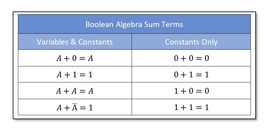
The sum terms are commonly known as max terms and represent the sum of all variables and/ or constants with and without inversion. The following table illustrates the possible states of the OR (Sum) function on variables and constants.
With the application of the following laws, any Boolean sum (OR) can be reduced to a single variable or constant. A brief description of each is given and “A” represents an input variable.
Annulment Law
OR operation of a term with 1 is always equal to 1 i.e. A+1 = 1
Complement Law
OR operation of a term with its complement is always equal to 1 i.e. A+A’ = 1
Commutative Law
The OR operation is independent of the order of terms i.e. A+1 = 1+A
Idempotent Law
The OR operation of a term with itself is always equal to the term i.e. A+A = A
Identity Law
The OR operation of a term with 0 is always equal to the term i.e. A+0 = A
The Product (AND) Term
In Boolean Algebra, product (multiplications) means resultant/ output of AND operation. The AND function is the mathematical equivalent of multiplication. The logical inputs are AND’ed together to yield a logical output. The inputs can be variables or constants.
Figure 2: The AND (Product) function with expression
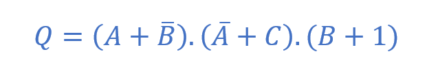
Product of Sum
In a nutshell, the OR function gives the logical sum of Boolean addition. Likewise, the AND function gives the logical product of Boolean multiplication. However, most digital circuits consist of multiple logic gates including AND, OR, and NOT gates which constitute combinational logic circuits. The combinational logic circuits are widely expressed as Sum-of-Product or Product-of-Sum as they include both AND, and OR functions, mainly.
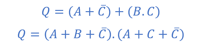
The Product-of-Sum (POS) expresses the combinational logic as two or more sums are multiplied together. In logical terms, the outputs of two or more OR functions (constituting sums) are connected to AND function (multiplied together) to give Product-of-Sum. It is an OR-AND logic operation having two or more OR terms and only one AND term. A few examples of Product-of-Sum (POS) are given below:
And,
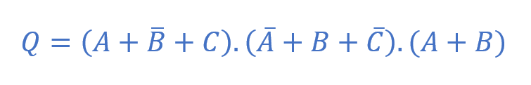
In the most cases, the Boolean expressions are given in the non-standard form of Product-of-Sum (POS) and can be converted into a standard Product-of-Sum (POS) form by applying distributive law with respect to the sum as shown below:
Applying distributive law with respect to sum:
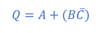
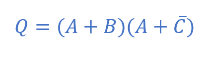
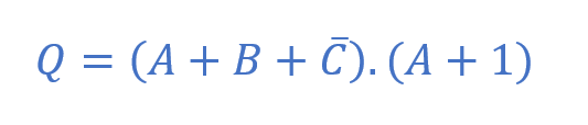
Another, non-standard POS form:
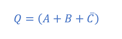
Which can be further reduced to:
Further to,
And,
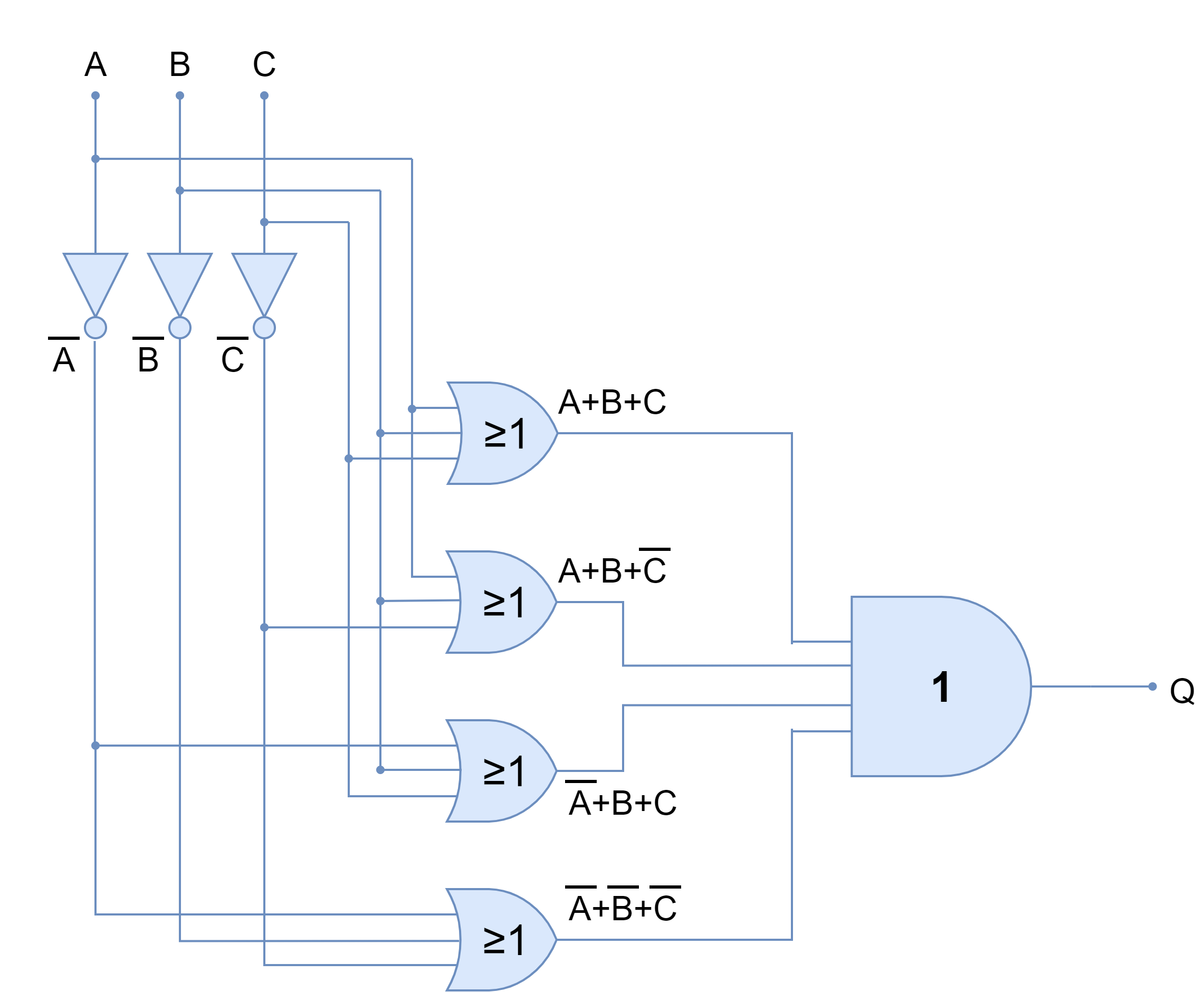
Constructing a Truth Table from Product-of-Sum (POS) Expression
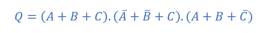
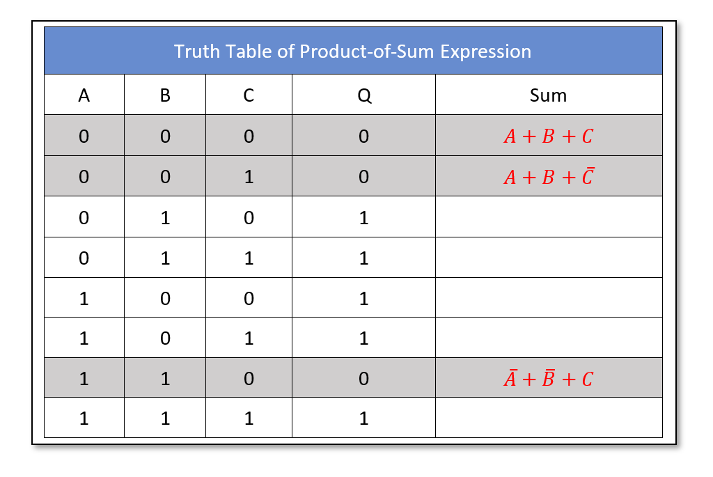
A truth table can be constructed from a product-of-sum expression and, conversely, a product-of-sum expression from a truth table. The sum terms in the product-of-sum expression, each produce a logic “0” for the specific input states. For example, the A+B+C term will produce a “0” state when A=1, B=1, & C=1. Similarly, A+B+C’ is “0” when A=1, B=1, & C=0. In a similar manner, the truth table is constructed for all the sum terms for the specific inputs’ states and their output is set to “0”. The output of all other states is set to “1”. Consider the following Boolean expression:
The following truth table is drawn for all of the possible states of A, B, and C. The output of the above expression is set to “0” for all the sums in terms of product-of-sum expression at their specific input states.
It is obvious from the above table that sum terms are set to “0” for that specific state of inputs and the rest of the output states are set to “1”. When any of the terms is “0” then AND (product) function sets the output to “0”.
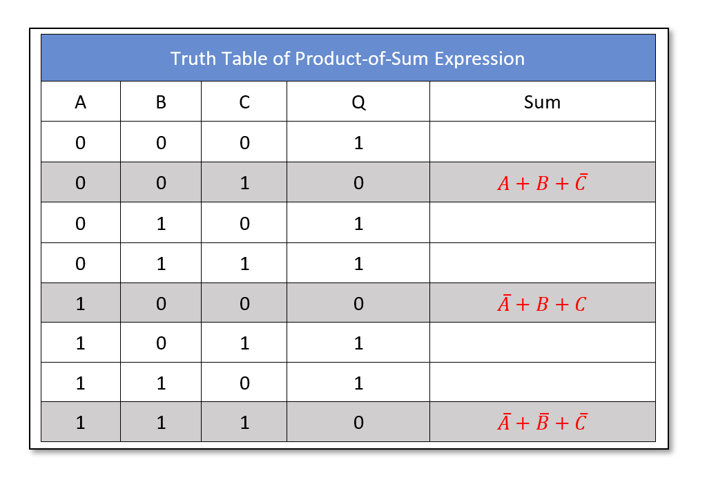
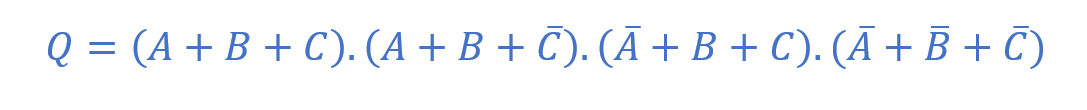
Likewise, a Boolean product-of-sum (POS) expression can be constructed from a given truth table. Consider the following truth tables.
From the above truth table, the following product-of-sum expression is derived.
Product-of-Sum Example
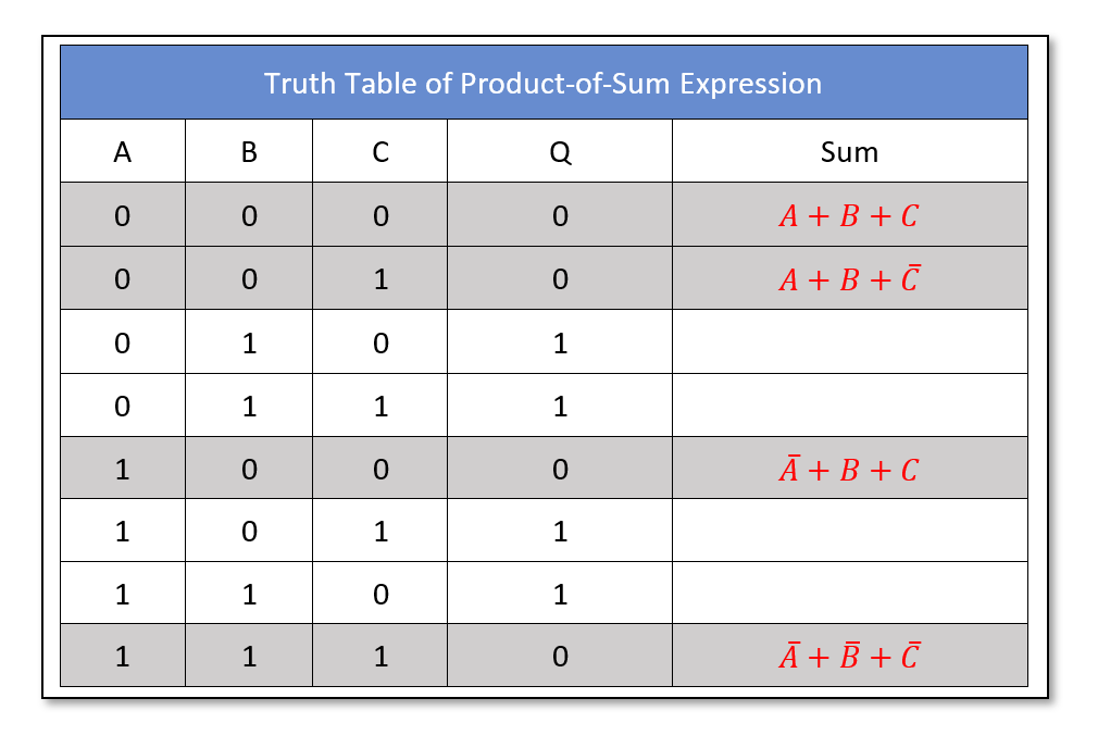
Consider the following given Boolean expression:
If the expression is in the non-standard form of the product-of-sum then it needs to be converted into standard form before proceeding further. The given expression is in standard form.
The following truth table is constructed from the above product-of-sum expression.
From the given product-of-sum following logic diagram is created.
Figure 3: The Logic Gate diagram of POS expression
Following the above example, from any truth table, a product-of-sum expression can be derived and can ease the process of creating a logic diagram.
Conclusion
A Product-of-Sum expression is a logical equivalent of two or more OR functions that are multiplied together. It is OR-AND logic which has more than two OR logics and only one AND logic.
In Boolean, the logical OR function performs addition and produces a Sum. Whereas, the logical AND function performs multiplication and produces a Product. In this way, the OR-AND logic is given the name of product-of-sum.
A maxterm is a sum term in a Boolean function in which every element is present either in complemented or in non-complemented form.
The combinational digital circuits consist of AND, OR, and NOT logic gates and are commonly described in product-of-sum (POS).
A truth table can be constructed easily from the given product-of-sum expression and vice versa.
In the truth table, the outputs are set to “0” for sum terms included in the product-of-sum- expression at that specific input state only, and the rest of the outputs are set to “1”.
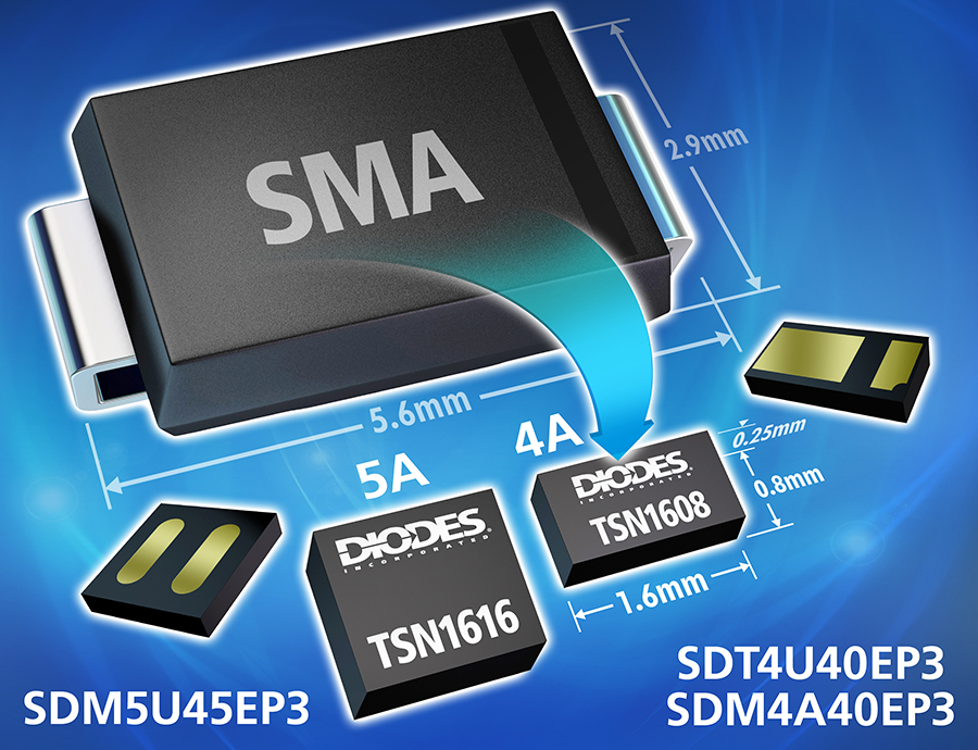
Diodes have announced the introduction of a series of high-current Schottky rectifiers in ultra-compact chip-scale packages (CSPs). The DIODESSDM5U45EP3 (5A, 45V), DIODES SDM4A40EP3 (4A, 40V), and DIODES SDT4U40EP3 (4A, 40V) achieve the industry’s highest current densities in their class, addressing market demands for smaller and more powerful electronic systems.
Each device can be employed for a variety of different purposes, serving as blocking or reverse-polarity protection diodes, electrical over-stress protection diodes, and free-wheeling diodes. The rectifiers in this series are designed for use in space-constrained applications – such as portable, mobile, and wearable devices, as well as IoT hardware.
The SDT4U40EP3 is the claimed industry’s smallest 4A trench Schottky rectifier, being the first ever in a 1608 package. It takes 90% less PCB area than competing devices. Its 800A/cm2 current density, also the highest for a trench Schottky in the industry, is due to its patent-pending innovative cathode design and manufacturing processes. The resulting ultra-low forward voltage performance (0.47V typical) minimises power losses, enabling the design of higher efficiency systems. Furthermore, its superior avalanche capability makes it robust enough to deal with extreme operating conditions, including transient voltages.
The X3-TSN1616-2 packaged SDM5U45EP3 has a 2mm2 footprint, while the 1.28mm2 footprint of the X3-TSN1608-2 packaged SDM4A40EP3 and SDT4U40EP3 enable system designers to maximise board real estate in modern, highly integrated consumer products. These ultra-thin CSPs, with their 0.25mm (typical) profiles, have shortened thermal paths – resulting in greater power dissipation, reducing thermal BOM costs and increasing reliability.
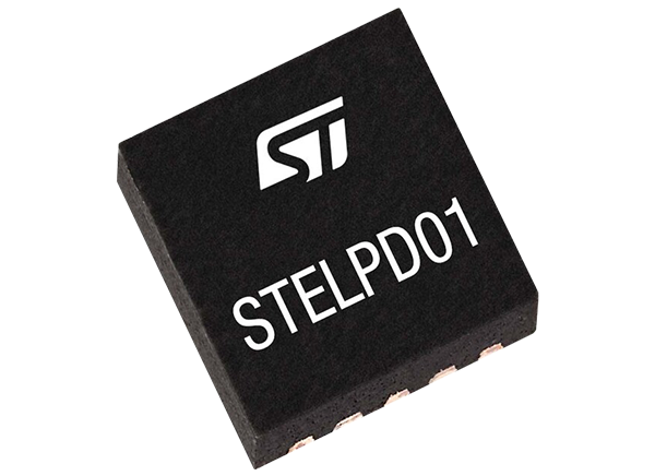
STMicroelectronics’ integrated electronic power switch precisely detects and reacts to overcurrent and overvoltage conditions
STMicroelectronics’ STELPD01 is an integrated electronic power switch for power rail protection applications. It is able to precisely detect and react to overcurrent and overvoltage conditions. When an overload condition occurs, the device goes into an open state, disconnecting the load from the power supply. An external power MOSFET can be driven to manage the power loss protection in case of a fault condition. In case of overvoltage on the input, the device regulates the output to a preset 17.5 V value.
Undervoltage lockout prevents the load from malfunctioning, keeping the device off if the rail voltage is too low. The STELPD01 features an adjustable turn-on slew rate, which is useful for keeping the in-rush current under control during startup and hot-swap operations.
Features
Wide input voltage range: 4 V to 18 V
17.5 V typical output overvoltage clamp
Absolute maximum voltage of 23.5 V
5 A maximum continuous current
Adjustable current limit with circuit breaker functionality
The SHS-X Handheld Oscilloscopes combines the functions of benchtop oscilloscope, multimeter, and recorder, including trend plot and waveform recorder, along with complex serial decoding/triggering, in isolated and non-isolated versions.
Saelig Company, Inc. has introduced the new and improved Siglent SHS-X Handheld Two-channel Digital Oscilloscopes, which are available in 100MHz and 200MHz analog bandwidths and isolated or non-isolated versions, with 1GSa/s sample rate and 12Mpts memory depth. The SHS800X versions have two non-isolated scope channels and one isolated multimeter channel, while the SHS1000X models feature full isolation: between the two oscilloscope channels, the multimeter channel, the power adapter, and the USB host/device port. The maximum analog voltage input for the isolated SHS1000X channels is CATIII 600 Vrms, CATII 1000 Vrms. For all SHS-X models, the maximum input for the multimeter channel is CATIII 600 Vrms, CATII 1000 Vrms.
Based on the success of Siglent’s previous SHS portable scopes, the new -X series adds increased memory depth, a faster waveform capture rate of 100,000 wfm/s, timebase down to 1ns/div, enhanced triggering choices (Edge, Slope, Pulse Width, Window, Runt, Interval, Dropout, Pattern, Video), serial trigger decoding (I2C, SPI, UART, CAN, LIN), improved FFT precision, and waveform recording of up to 50MB internal or 2GB external. The user-friendly front panel design allows quick access to most of the commonly used scope functions. The SHS810X is the 100MHz version and the SHS820X is the 200MHz version of non-isolated scopes, while the SHS1102X is the 100MHz version and the SHS1202X is the 200MHz version of the fully-isolated version.
One of the great advantages of a portable oscilloscope is its ability to make safe, floating, non-ground-referenced measurements. Inputs can safely be connected to a circuit under investigation without regard to polarity, as long as the voltage and current limitations are observed. Full isolation also reduces the risk of accidental short-circuit equipment damage.
Designed and manufactured by leading test instrument company Siglent Technologies, the SHS-X Series of portable oscilloscopes offer benchtop specs, are compact (10.25” x 6.43” x 2.1”) and lightweight (3.3lb), and are available now from their technical distributor Saelig Company, Inc.
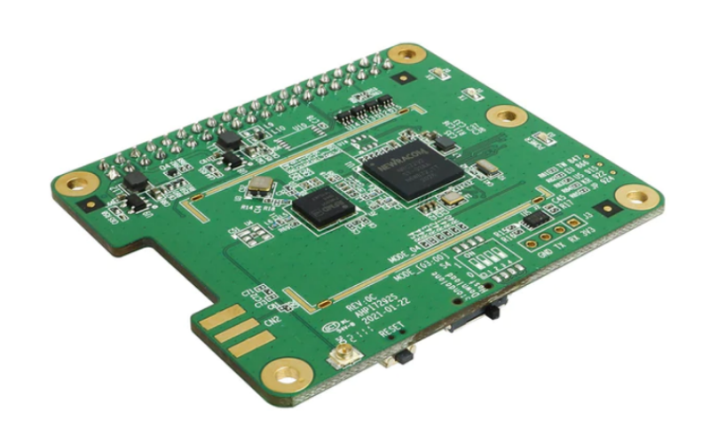
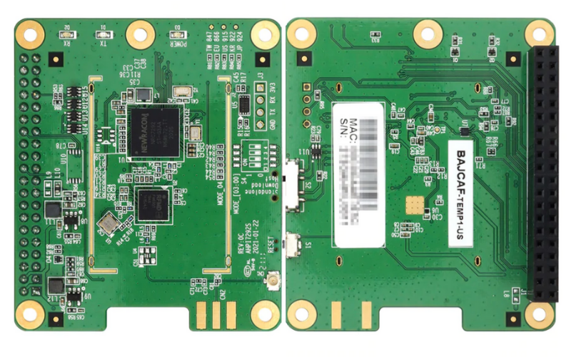
Taipei City-based electronic embedded design manufacturer, Alfa Network, has designed the “industry’s first” IEEE802.11ah sub 1 GHz module in the Raspberry Pi HAT form factor. There have been several Wi-Fi Raspberry Pi HATs in the market, but this AHPI729S module will serve long-range connectivity for IoT applications such as Industry 4.0 and edge AI. Providing communication channels in the sub-GHz frequency range, Alfa Network’s AHPI729S will offer 847, 866, 915, 922, and 924 MHz channels. However, it is important to note that these frequencies will depend on the country of residence.
At the heart of the wireless connectivity module for Raspberry Pi is the Newracom NRC7292 Wi-Fi HaLow SoC, which operates in the sub 1GHz license-exempt band offering a much wider range than the existing 2.4 and 5GHz wireless technologies. The radio transceiver integrated circuit NRC7292 is designed in such a way that it requires minimum external circuits and reduces the time to market.
With the dual embedded ARM CortexM0 and Cortex-M3 processor, the NRC7292 module can be used either as a standalone or a slave to a host processor via a serial peripheral interface (SPI) or universal asynchronous receiver transmitter (UART) interface. In addition, it can support both AP and STA roles.
Specifications of Wi-Fi HaLow Raspberry Pi HAT
SoC: Newracom NRC7292
CPU: Arm Cortex-M3 for application processing and Arm Cortex-M0 for WLAN
Memory: 32kB Boot ROM for each M0 and M3 processor, and 752kB system SRAM
As the industry’s first Wi-Fi HaLow Raspberry Pi HAT, there is expected traction on the hardware. Until now, developers were limited to not using Wi-Fi HaLow networking on their Raspberry Pi single-board computers, however, there will be a change in paradigm with the public availability of Alfa Network’s AHPI729S module. Developers who are looking to develop applications using IEE802.11ah Wi-Fi on your favorite Raspberry Pi single-board computer, this HAT is for you!
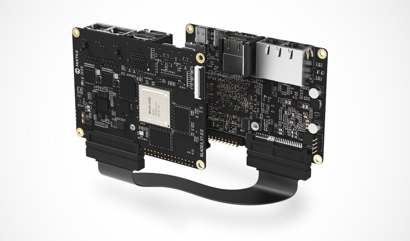
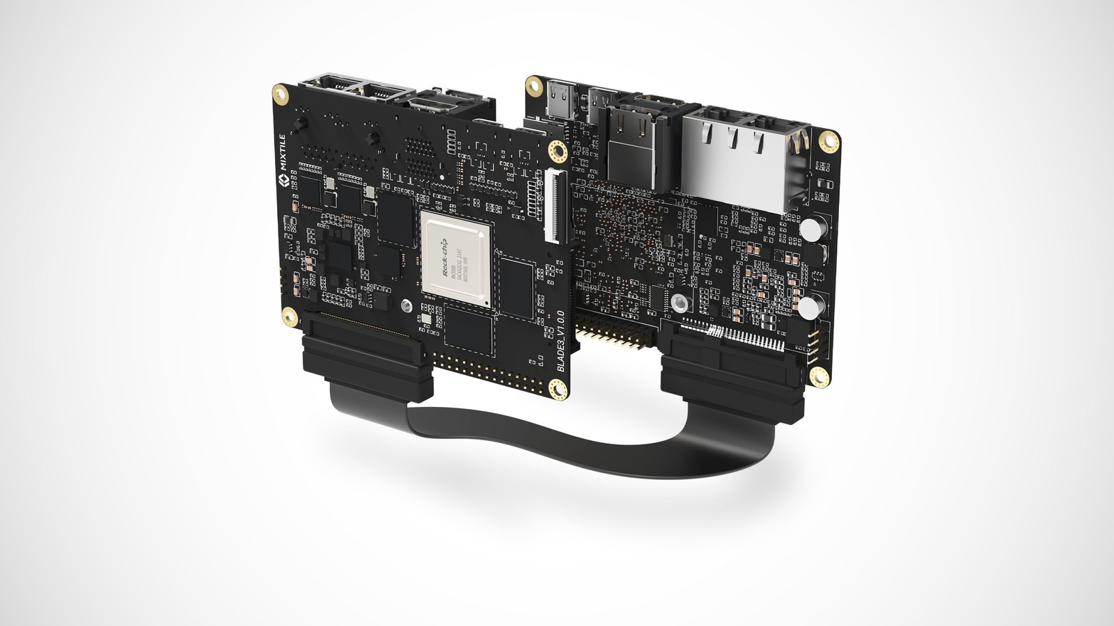
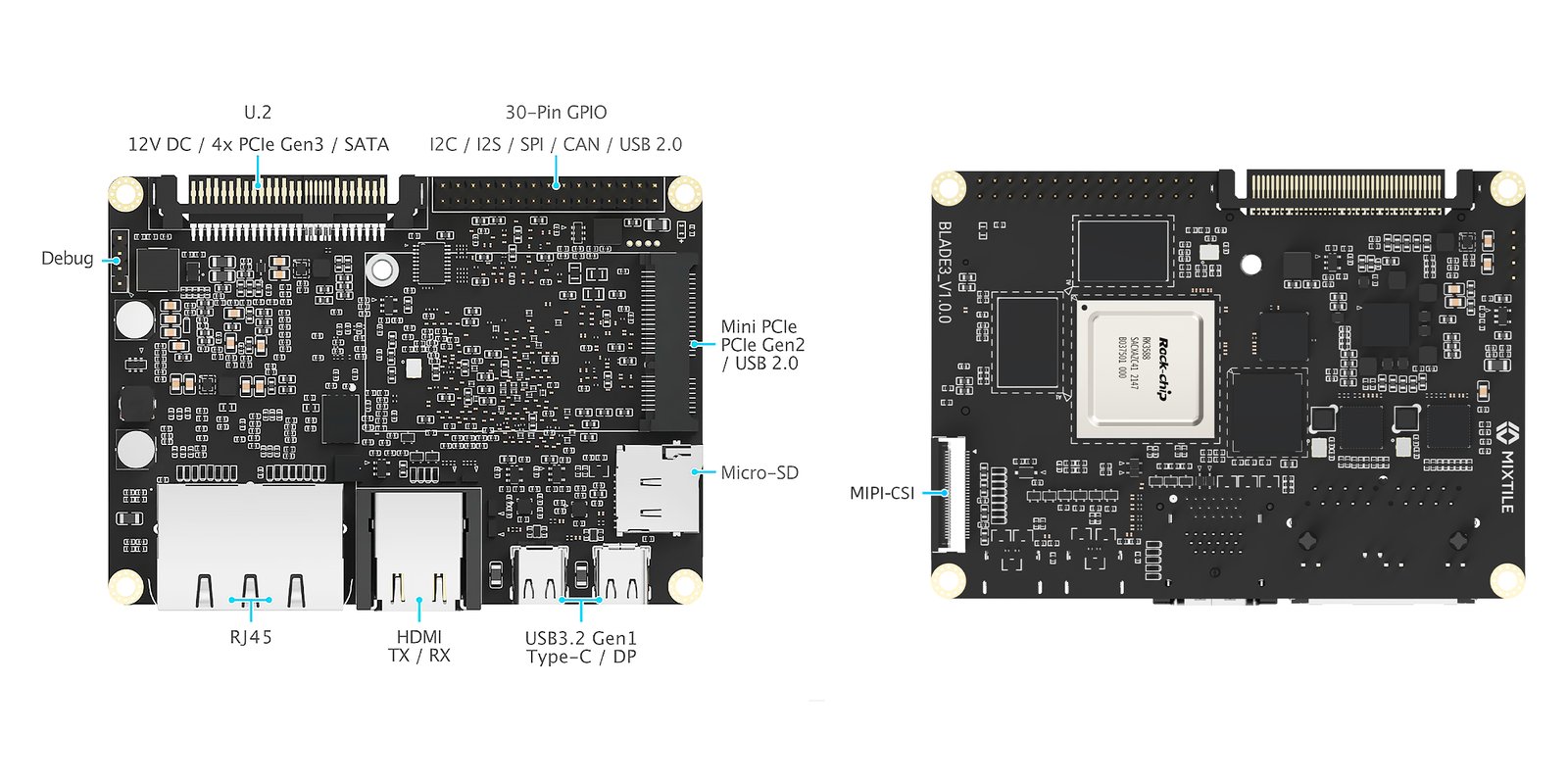
A new single-board computer is hitting crowdfunding very soon! Shenzhen-based embedded device manufacturer Mixtile Limited has unveiled details on its latest Mixtile Blade 3 single-board computer powered by the Rockchip RK3588 system on chip in Pico-ITX form factor. This high-performance stackable board is designed for the rapid development and prototyping of AI applications at the edge networks. The Mixtile Blade 3 can act as an edge computing hardware, enabling developers to deploy the hardware at edge locations with low-power consumption and enhanced performance.
At the heart of the Mixtile Blade 3 is the RK3588 SoC, a low-power, high-performance processor based on an Arm instruction set for PC and edge computing devices for multimedia applications. Rockchip RK3588 is equipped with a quad-core Cortex-A76 and a quad-core Cortex-A55 processor with a NEON co-processor on board. The SoC supports powerful video encoding and decoding techniques including H.265 and VP9 decoder by 8K at 60 frames per second, H.264 decoder by 8K at 30 frames per second, and many other decoder models. The system-on-chip comes with a 48-megapixel image signal processor that can implement several algorithm accelerators such as HDR, 3A, 3DNR, sharpening, dehaze, fisheye correction, and gamma correction.
Mixtile Blade 3 runs a hybrid Android and Linux distribution that operates Android 12 within a Linux container because of its prolific driver support, making the software development process easy. The hardware will be shipped with a preloaded Android 12 operating system allowing developers to take full advantage of the board’s hardware features. Specially designed for embedded edge applications, the Mixtile Blade 3 edge device fills the gap between traditional operating systems and a complete solution with hybrid distribution for improved security and performance.
Previously, available for pre-order from $160 to $259 depending on the variant of the LPDDR4 memory and eMMC storage. However, the manufacturer has currently closed the first round of pre-orders and will be announcing the next pre-order round very soon with no tentative date. Based on the listing on Crowdsupply, we can assume that the edge device will soon be available for crowdfunding with several pledging options. There is no announcement on the date of the launch of the hardware on Crowdsupply, but interested folks can register themselves on the product page to get notified when the product goes live.
From medium to small-scale enterprise applications, Mixtile Blade 3 is a user-friendly option to explore the scope for real-time edge data processing. For the quickly revolutionizing Industry 5.0, this development board provides opportunities for highly efficient projects delivering optimized performance to become an ideal solution for industrial settings.
Analysis
The Pico-ITX 2.5-inch carbon footprint edge device is equipped with one of the latest Rockchip SoC designed for edge applications. Recently, we have witnessed a lot of development around the RK3588 system-on-chip that is being integrated with many embedded hardware devices. Rich connectivity and support for advanced video encoding/decoding techniques make it suitable for high-end multimedia applications. “From Servers to Custom Clusters to Big Data Storage, Mixtile Does it All!” the company says it makes it an ideal HPC cluster node for ultra-low-power consumption. More details can be found on the official product page and Crowdsupply.
Doogee started 2022 with Doogee V20, then followed it with the successful S98 model. Doogee is now introducing its new S98 Pro, the rugged phone with thermal imaging, as a successor to the S98.
The S98 Pro comes out strong with an alien-inspired design. The shape of the camera bump combined with the thin slender lines on the back of the cover combines to illustrate the figure of the out-earthers.
The rugged phone is believed to have the best camera setup. The phone pairs a 48MP main camera with a 20MP night vision camera. Put that together with a thermal imaging sensor, and you have a camera set that can capture images in all situations. The night vision detects anything that reflects infrared light, whereas the thermal vision detects anything that emits heat.
The new rugged phone will use the InfiRay thermal sensor. With the highest thermal resolution of 256×192, it brings more than twice the number of thermal pixels as other sensors. Combining that with a 25Hz high frame rate, it produces images that are so clear it can accurately detect draught, dampness, leaks, electric short, blockages, and elevated temperatures.
The coolest thing about this thermal sensor is a technology called Dual Spectrum Fusion Algorithm. This tech allows images from the thermal sensor and the primary sensor to be placed over each other. Then you have a level that will let you adjust how much thermal detail transparency level you want over the actual image. This will allow you to accurately trace a problem spot.
We will keep you updated with news about the rest of the features as we get them. The company also confirms Doogee S98 Pro will available for purchase in early June. You can learn more about this product from the official Doogee S98 Pro website.
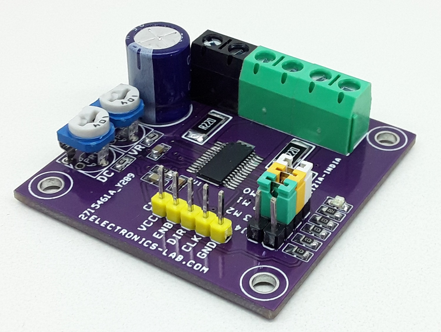
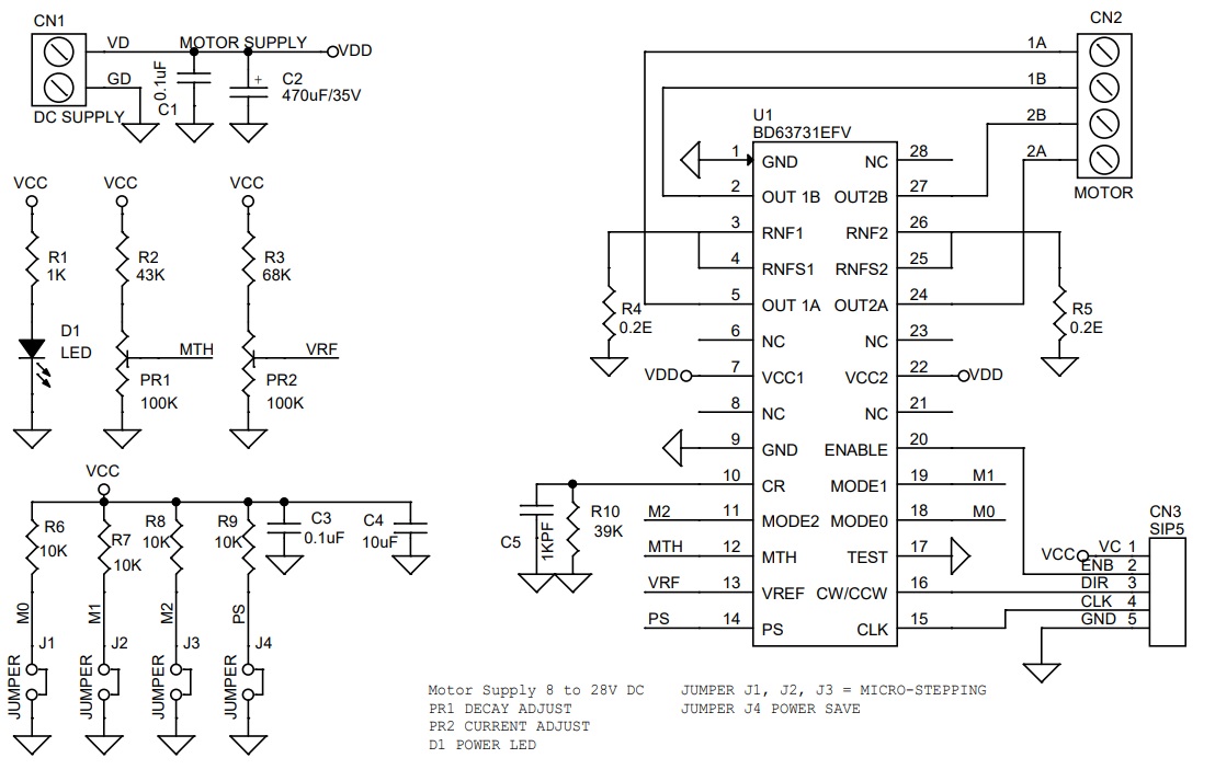
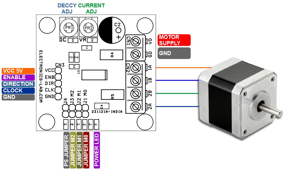
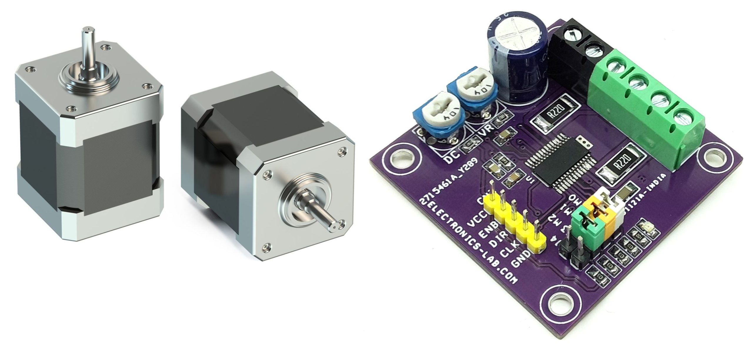
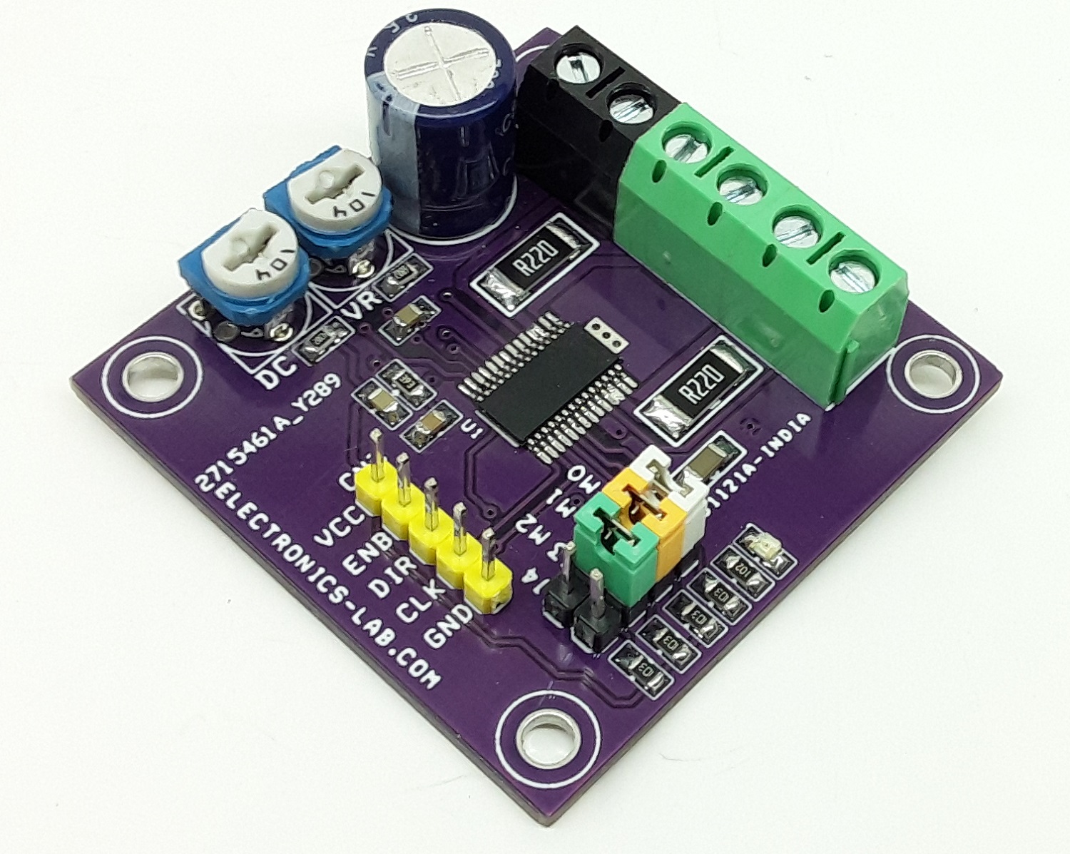
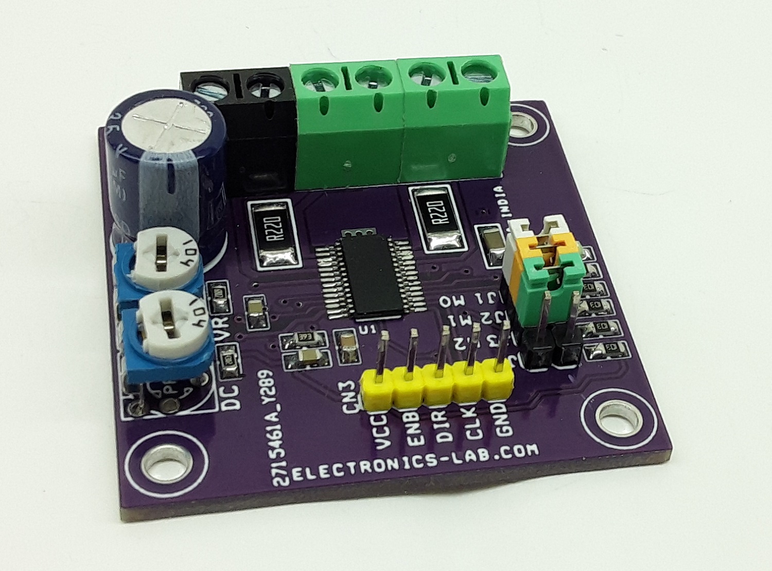
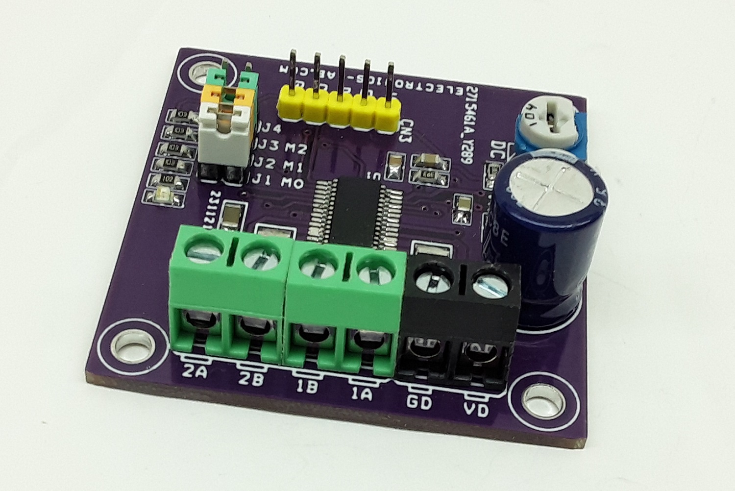
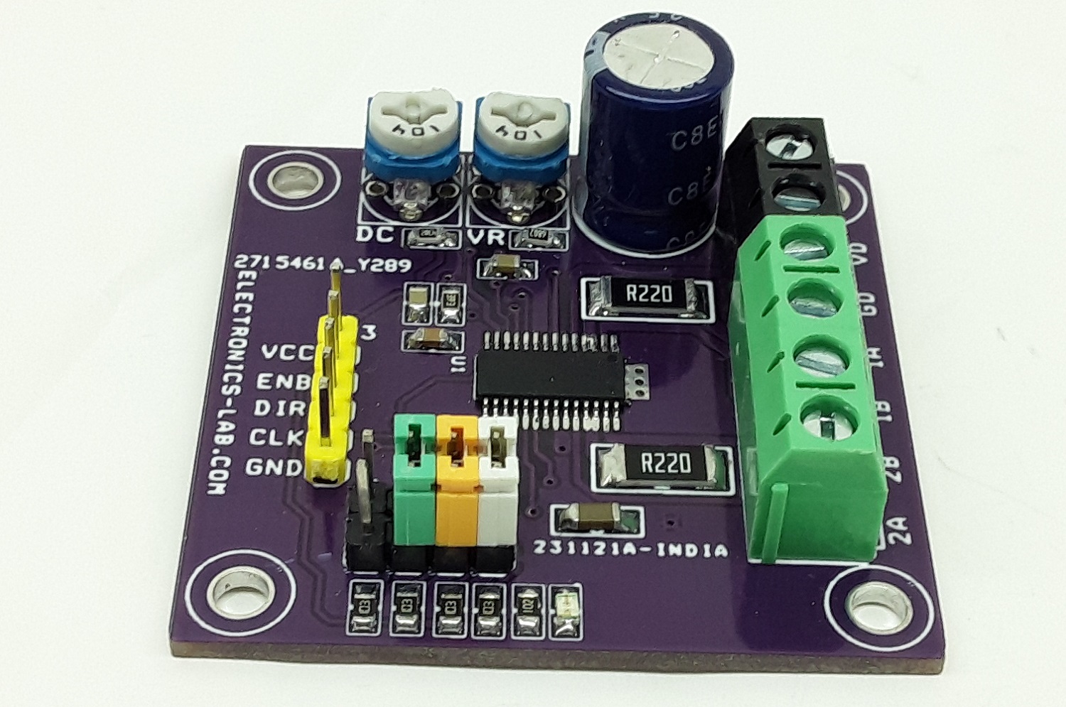
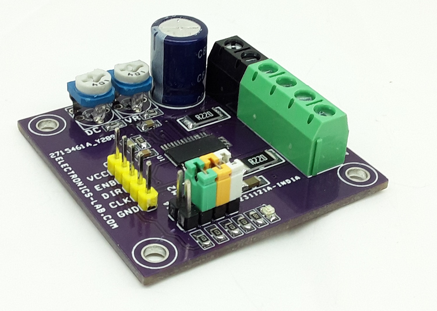
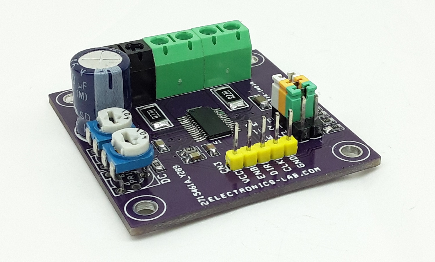
The project presented here is a bipolar stepper motor driver. It is based on BD63731EFV chip which is a low-consumption driver that is driven by a PWM signal. The power supply voltage of the project is 8 to 28V DC, and the rated output current is 3A. CLK-IN driving mode is adopted for the input interface, and excitation mode is corresponding to FULL STEP mode (2 types), HALF STEP mode (2 types), QUARTER STEP mode (2 types), 1/8 STEP mode, and 1/16 STEP mode via a built-in DAC. In terms of current decay, the SLOW DECAY/FAST DECAY ratio may be set without any limitation, and all available modes may be controlled in the most appropriate way. In addition, the power supply may be driven by one single system, which simplifies the design.
Note: Refer to datasheet of BD63731EFV chip for input signals, timing chart and micro-stepping chart.
Features
Motor Supply 8 to 28V DC
Rated Output Current 3.0 A
Low ON Resistance DMOS Output
CLK-IN Drive Mode
PWM Constant Current (other oscillation)
Built-in Spike Noise Cancel Function (external noise filter is unnecessary)
PR2 Trimmer Potentiometer: Motor Current Adjustment = 0 to 3V
Jumper J4 PS/Power Save Jumper J4
The PS pin can make circuit in standby state and make motor output OPEN. In the standby state, the translator circuit is RESET (initialized) and the electrical angle is initialized. When PS=L to H, be careful because there is a delay of 40 μs (Max) before it is returned from standby state to normal state and the motor output becomes ACTIVE
PR1 Trimmer Potentiometer: Decay Adjust
0 to 0.3V Slow Decay
4V to 1V Mix Decay
5V to 2V Fast Decay
1V to 3.5V Auto Decay
SLOW DECAY
The output current ripple is small and this is favorable for keeping motor torque high because the voltage between the motor coils is small and the regenerative current decreases slowly. However, an increase in the output current due to deterioration of the current control in the lower current operation in HALF STEP, QUARTER STEP, 1/8 STEP, 1/16 STEP, due to the influence of the motor reverse electromotive voltage during high pulse rate driving in the mode, the current waveform is not able to follow the change in the current limit and the distortion and motor vibration increases. Thus, this decay mode is suited to FULL STEP mode or low-pulse-rate driven HALF STEP, QUARTER STEP, 1/8 STEP or 1/16 STEP modes.
FAST DECAY
Fast decay decreases the regeneration current much more quickly than slow decay, reducing distortion of the output current waveform. However, fast decay yields a much larger output current ripple, which decreases the overall average current running through the motor. This causes two problems: first, the motor torque decreases (increasing the current limit value can help eliminate this problem, but the rated output current must be taken into consideration); and second, the power loss within the motor increases and thereby radiates more heat. If neither of these problems is of concern, then fast decay can be used for high-pulse rate HALF STEP, QUARTER STEP, 1/8 STEP or 1/16 STEP drive. Additionally, this IC allows for MIX DECAY mode/AUTO DECAY mode that can help to improve upon problems that arise from using fast or slow decay.
MIX DECAY
During current decay Switching between SLOW DECAY and FAST DECAY can improve current control without increasing the current ripple. In addition, the time ratio of SLOW DECAY and FAST DECAY can be changed by the voltage input to the MTH pin, and it is possible to achieve an optimal control state for any motor. During MIX DECAY mode about chopping cycle, the first (t1 to t2) of which operates the IC in SLOW DECAY mode, and the remainder (t2 to t3) of which operates in FAST DECAY mode. However, if the output current does not reach the set current limit during the first (t1 to t2) decay period, the IC operates in fast decay mode only.
AUTO DECAY
Current control capability can still be improved without making the current ripple big by using SLOW DECAY and switches only to FAST DECAY when required. Decay mode becomes FAST DECAY only when output current reaches the set value while at minimum ON time.
Protection Circuits
1.Thermal Shutdown (TSD)
This IC has a built-in thermal shutdown circuit for thermal protection. When the IC’s chip temperature rises 175 °C (Typ) or more, the motor output becomes OPEN. Also, when the temperature returns to 150 °C (Typ) or less, it automatically returns to normal operation. However, even when TSD is in operation, if heat is continued to be added externally, heat overdrive can lead to destruction.
2. Over Current Protection (OCP)
This IC has a built-in over current protection circuit as a provision against destruction when the motor outputs are shorted each other or VCC-motor output or motor output-GND is shorted. This circuit latches the motor output to OPEN condition when the regulated current flows for 4 μs (Typ). It returns with power reactivation or a reset by the PS pin. The over current protection circuit’s only aim is to prevent the destruction of the IC from irregular situations such as motor output shorts, and is not meant to be used as protection or security for the set. Therefore, sets should not be designed to take into account this circuit’s functions. After OCP operating, if irregular situations continue and the return by power reactivation or a reset by the PS pin, then OCP operates repeatedly and the IC may generate heat or otherwise deteriorate. When the L value of the wiring is great due to the wiring being long, the motor outputs are shorted each other or VCC-motor output or motor output-GND is shorted., if the output pin voltage jumps up and the absolute maximum values can be exceeded after the over current has flowed, there is a possibility of destruction. Also, when current which is the output current rating or more and the OCP detection current or less flows, the IC can heat up to Tjmax=150 °C exceeds and can deteriorate, so current which or more the output rating should not be applied.
3. Under Voltage Lock Out (UVLO)
This IC has a built-in under voltage lock out function to prevent false operation such as IC output during power supply under voltage is low. When the applied voltage to the VCCX pin goes 5 V (Typ) or less, the motor output is set to OPEN. This switching voltage has a 1 V (Typ) hysteresis to prevent false operation by noise etc. Be aware that this circuit does not operate during power save mode. Also, the electrical angle is reset when he UVLO circuit operates.
4. Over Voltage Lock Out (OVLO)
This IC has a built-in over voltage lock out function to protect the IC output and the motor during power supply over voltage. When the applied voltage to the VCCX pin goes 32 V (Typ) or more, the motor output is set to OPEN. This switching voltage has a 1 V (Typ) hysteresis and a 4 μs (Typ) mask time to prevent false operation by noise etc. Although this over voltage locked out circuit is built-in, there is a possibility of destruction if the absolute maximum value for power supply voltage is exceeded. Therefore, the absolute maximum value should not be exceeded. Be aware that this circuit does not operate during power save mode.
5. Protects against malfunction when power supply is disconnected (Ghost Supply Prevention Function)
If a control signal is input when there is no power supplied to this IC, there is a function which prevents a malfunction where voltage is supplied to power supply of this IC or other IC in the set via the electrostatic destruction prevention diode from these input pins to the VCCX. Therefore, there is no malfunction of the circuit even when voltage is supplied to these input pins while there is no power supply. (Note 1) control signal=CLK, CW_CCW, MODE0, MODE1, MODE2, ENABLE, PS, MTH, VREF
6. Operation Under Strong Electromagnetic Field
The IC is not designed for using in the presence of strong electromagnetic field. Be sure to confirm that no malfunction is found when using the IC in a strong electromagnetic field.
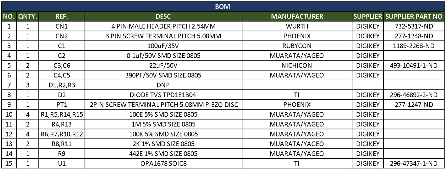
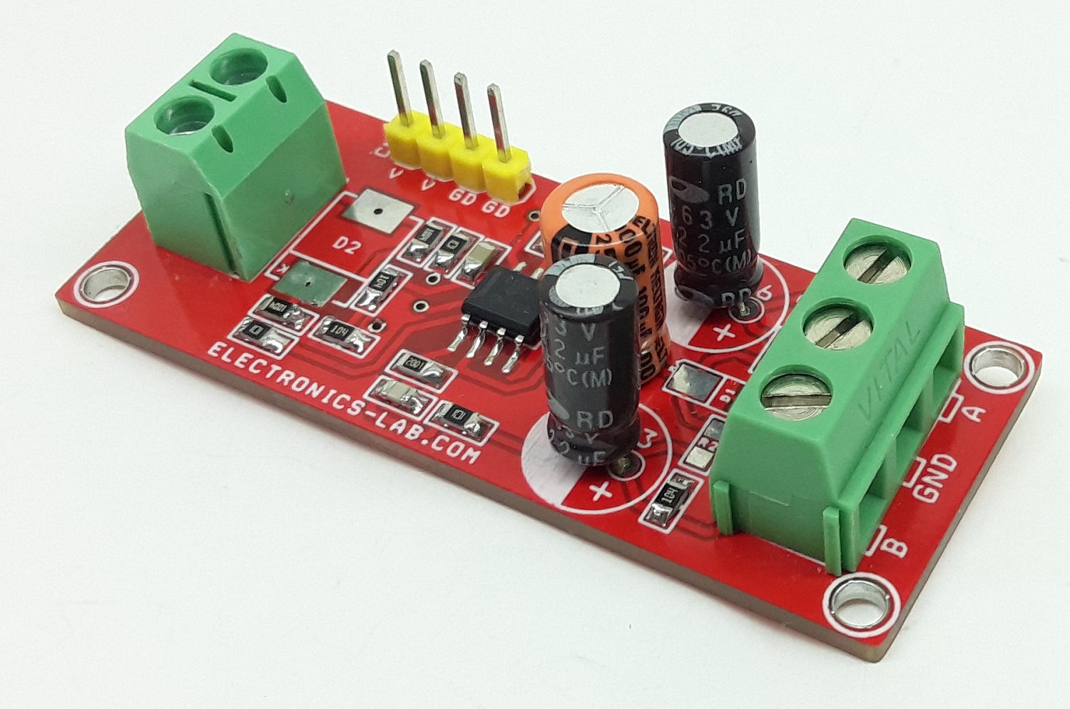
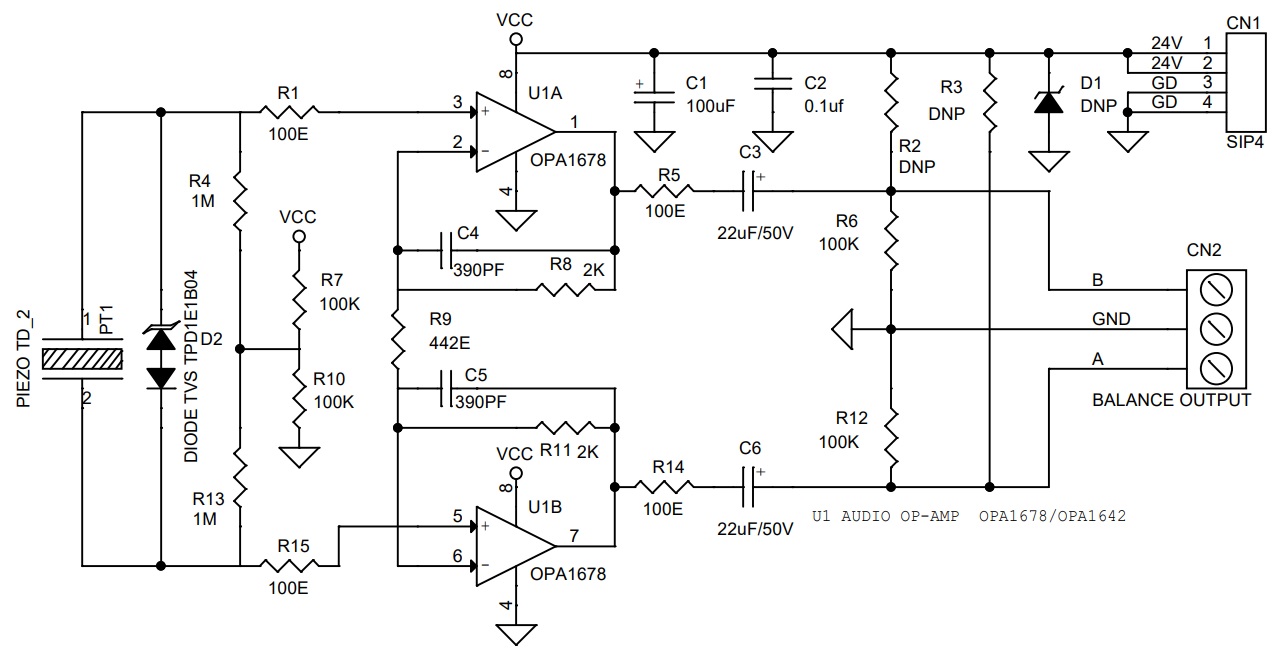
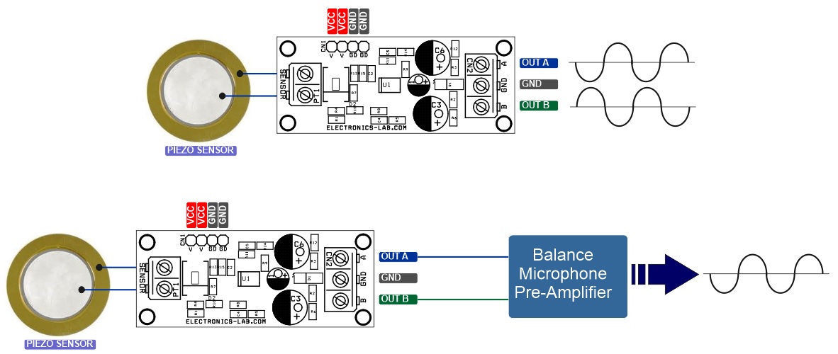
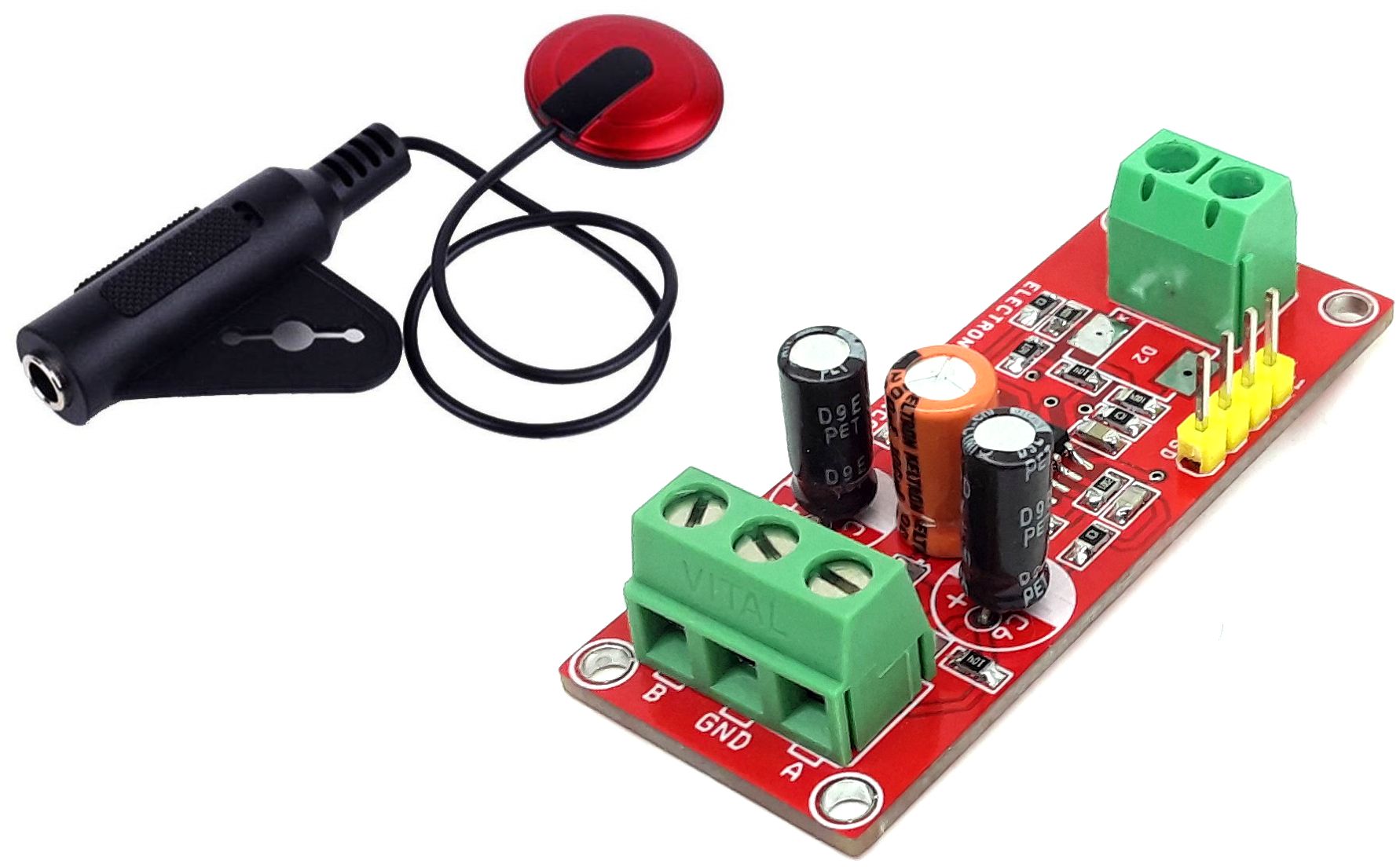
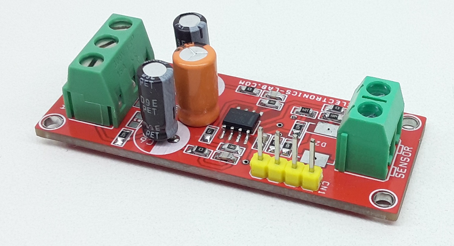
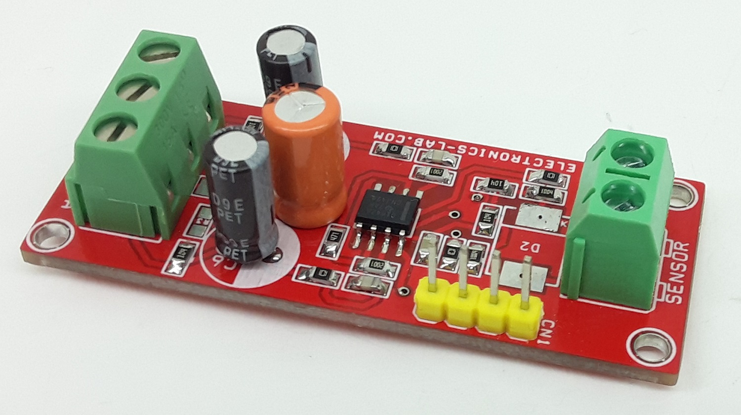
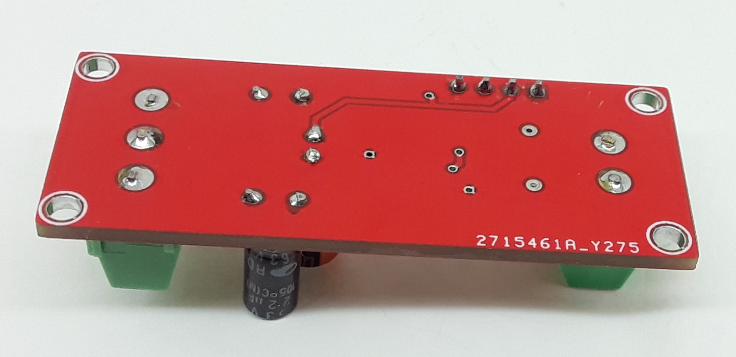
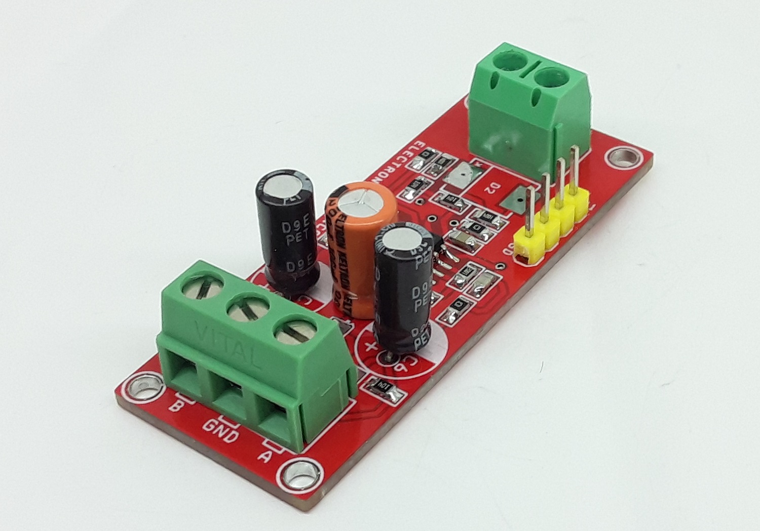
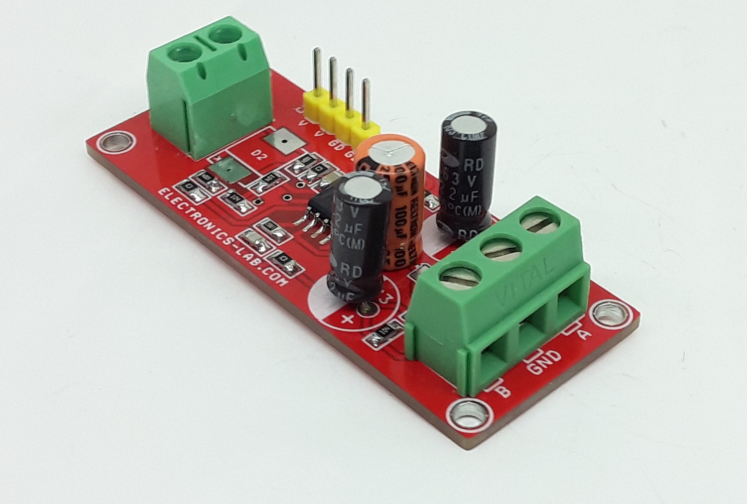
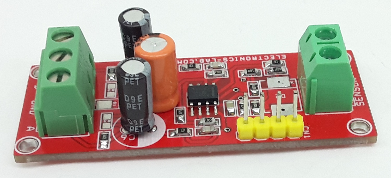
The board presented here is a preamplifier for contact microphones that are used for amplifying the sound of musical instruments which do not contain electrical pickups, such as guitar and violins. Most contact microphones use a piezo element to convert vibration in the body of the musical instrument to a voltage. The circuit is built using OPA1678 OPAMP. The low noise and low input bias current of the OPA1678 makes the device an excellent choice for high impedance preamplifiers for piezo elements. This preamplifier circuit provides high input impedance for the piezo element but has low output impedance for driving long cable runs. It provides a balanced audio output that can be fed to a balanced microphone pre-amplifier. The circuit has also the option for phantom power input. Install R3=1.2K Ohms, R2=1.2K Ohm and Zener diode 24V.