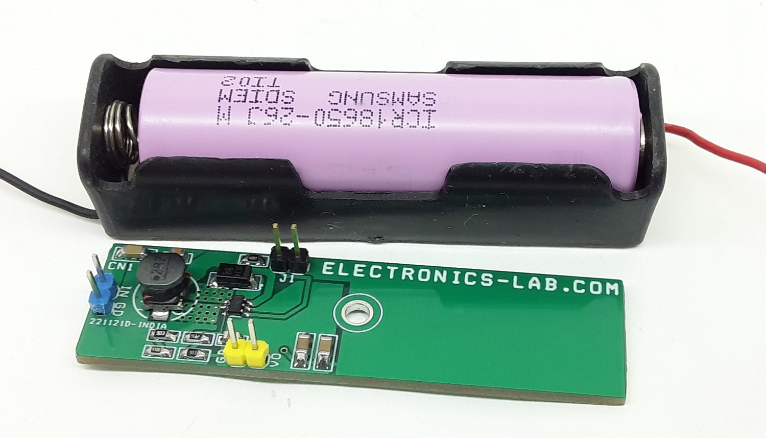
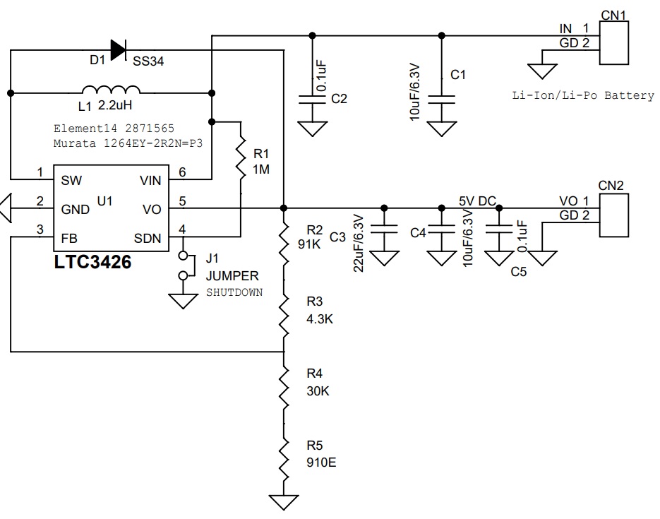
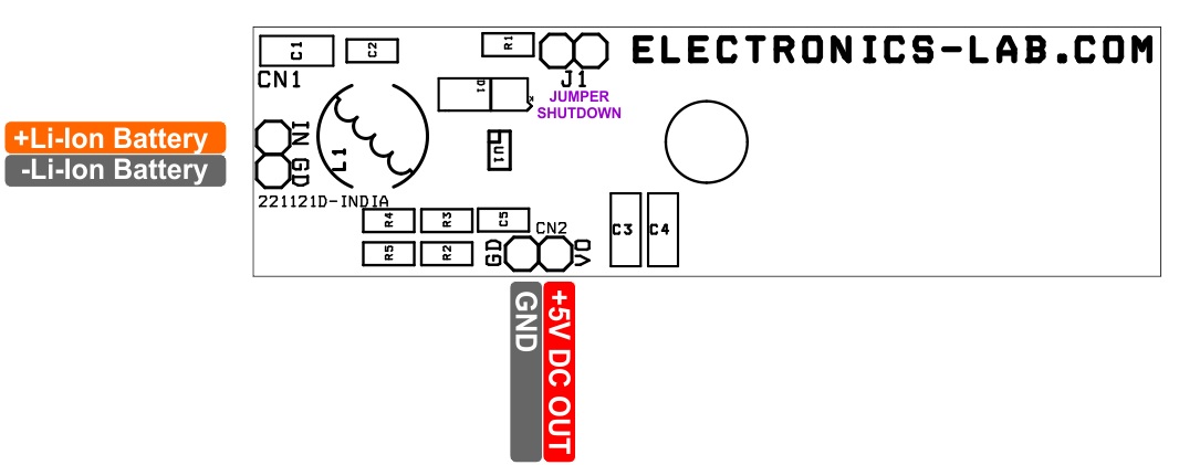
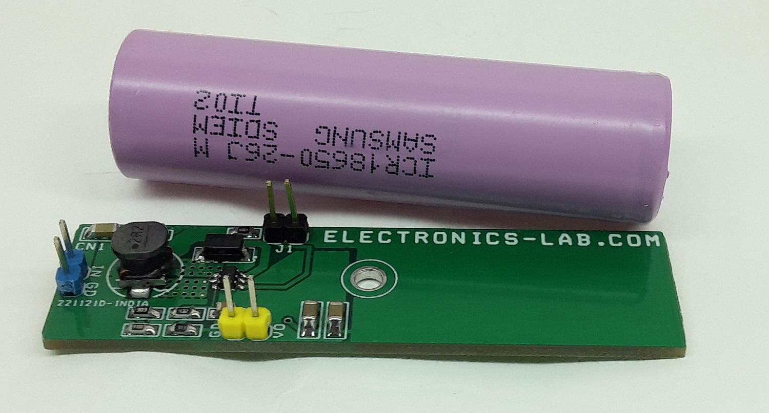
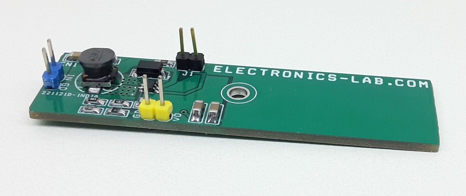
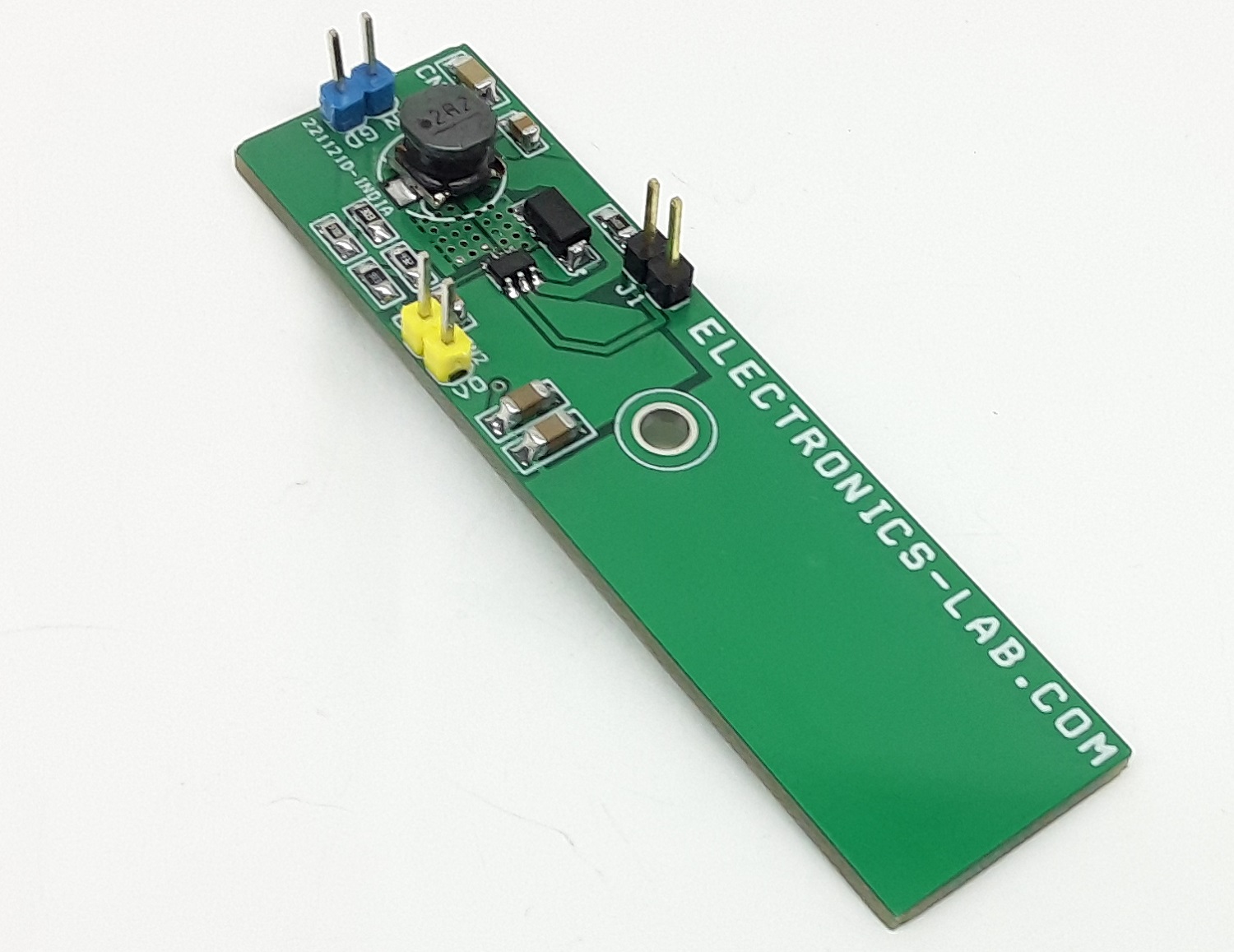
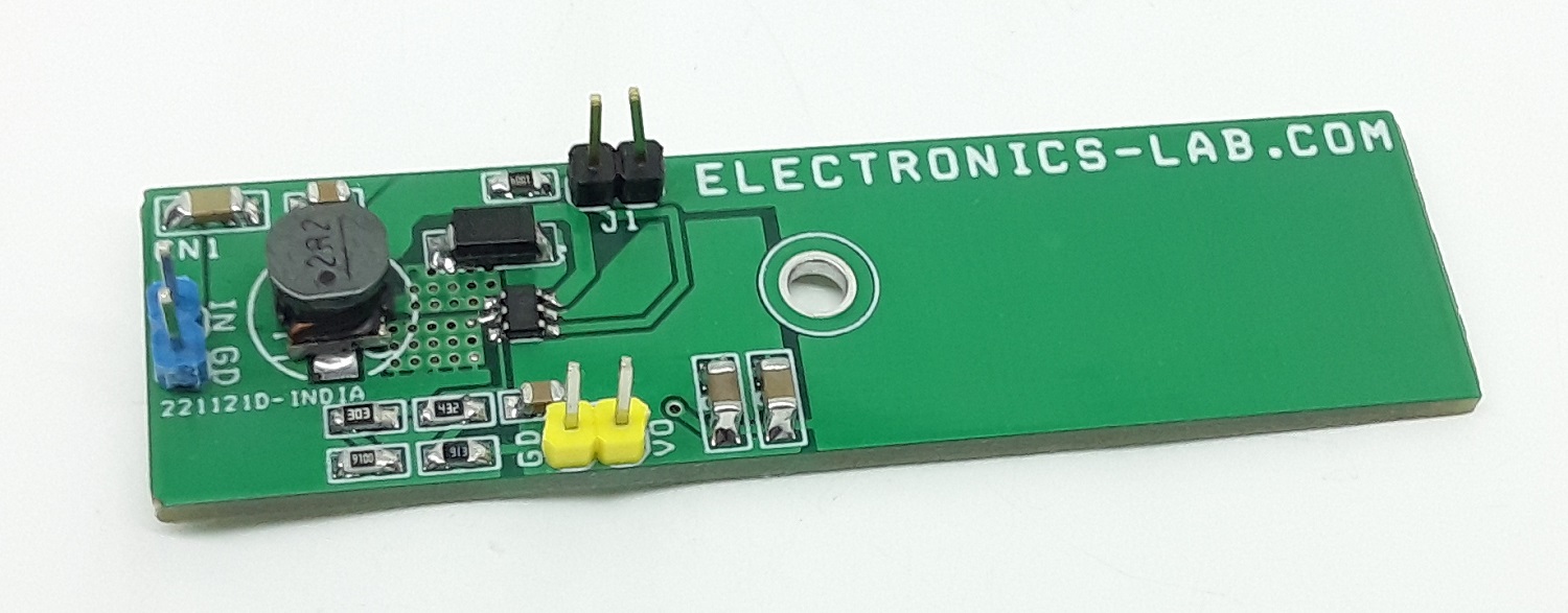
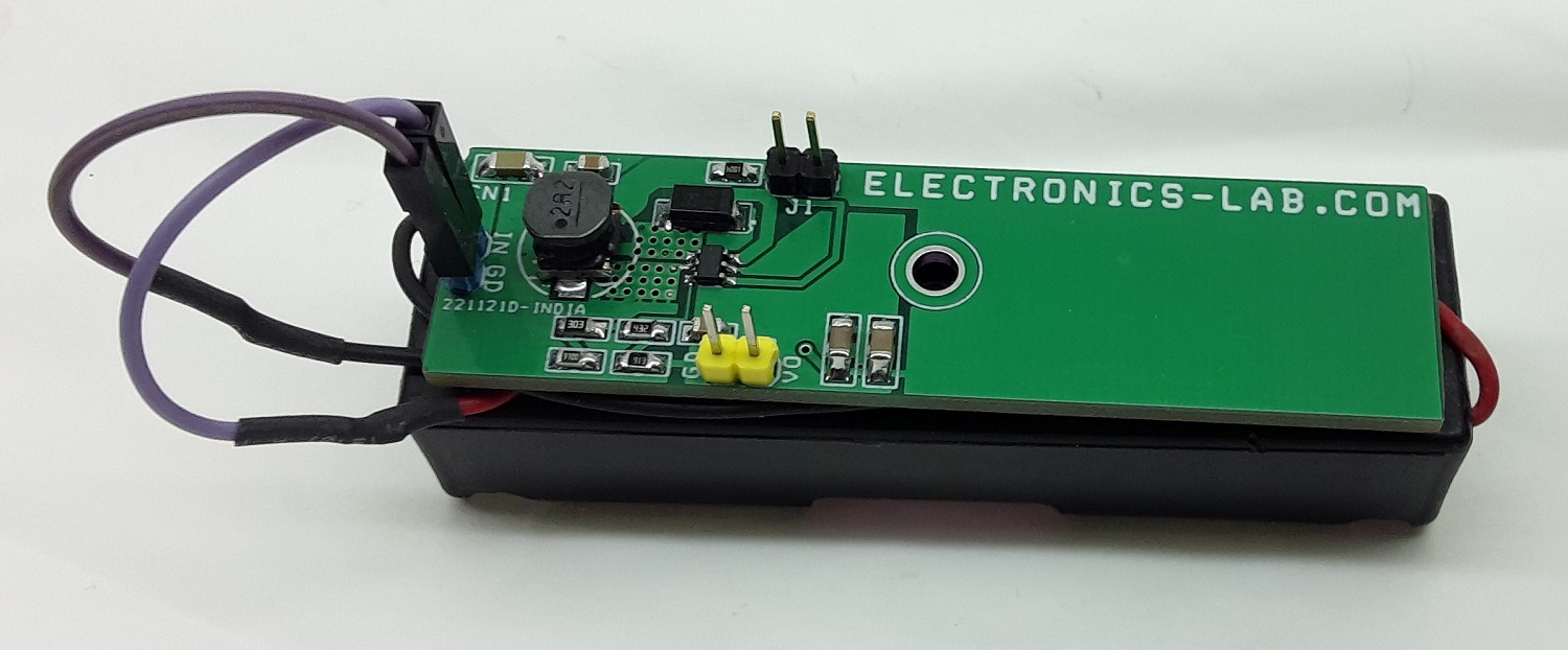
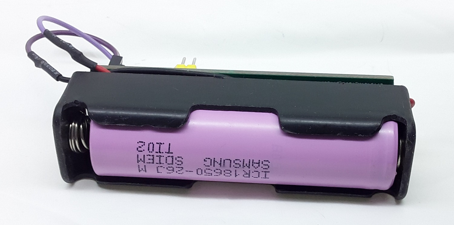
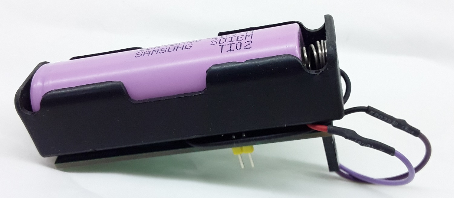
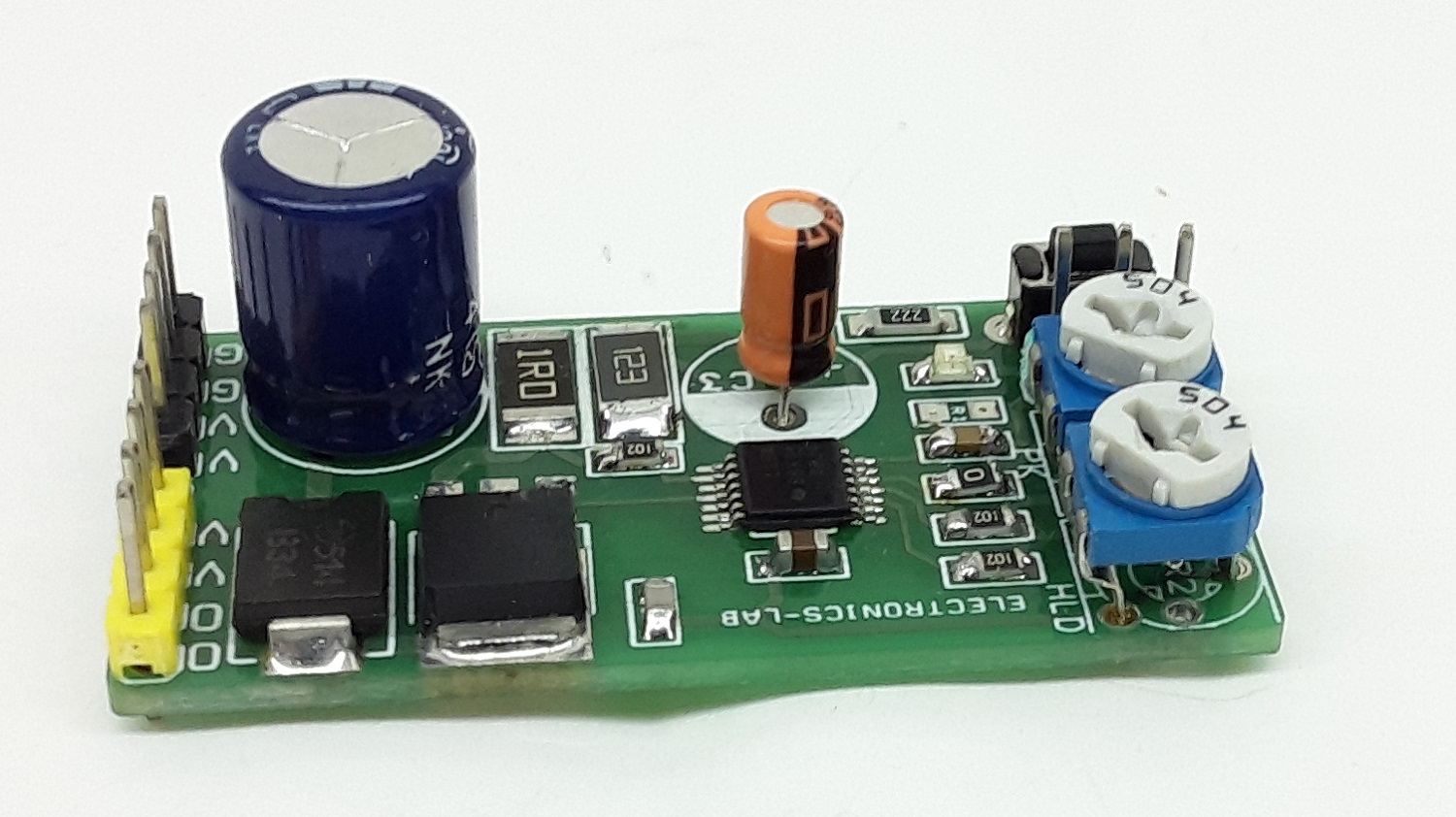
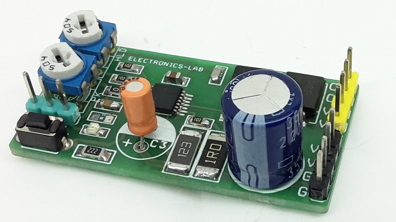
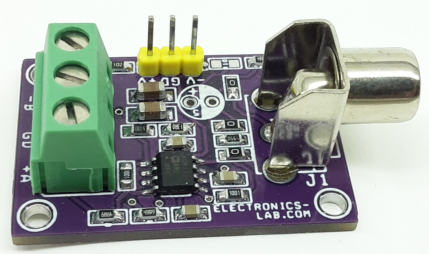
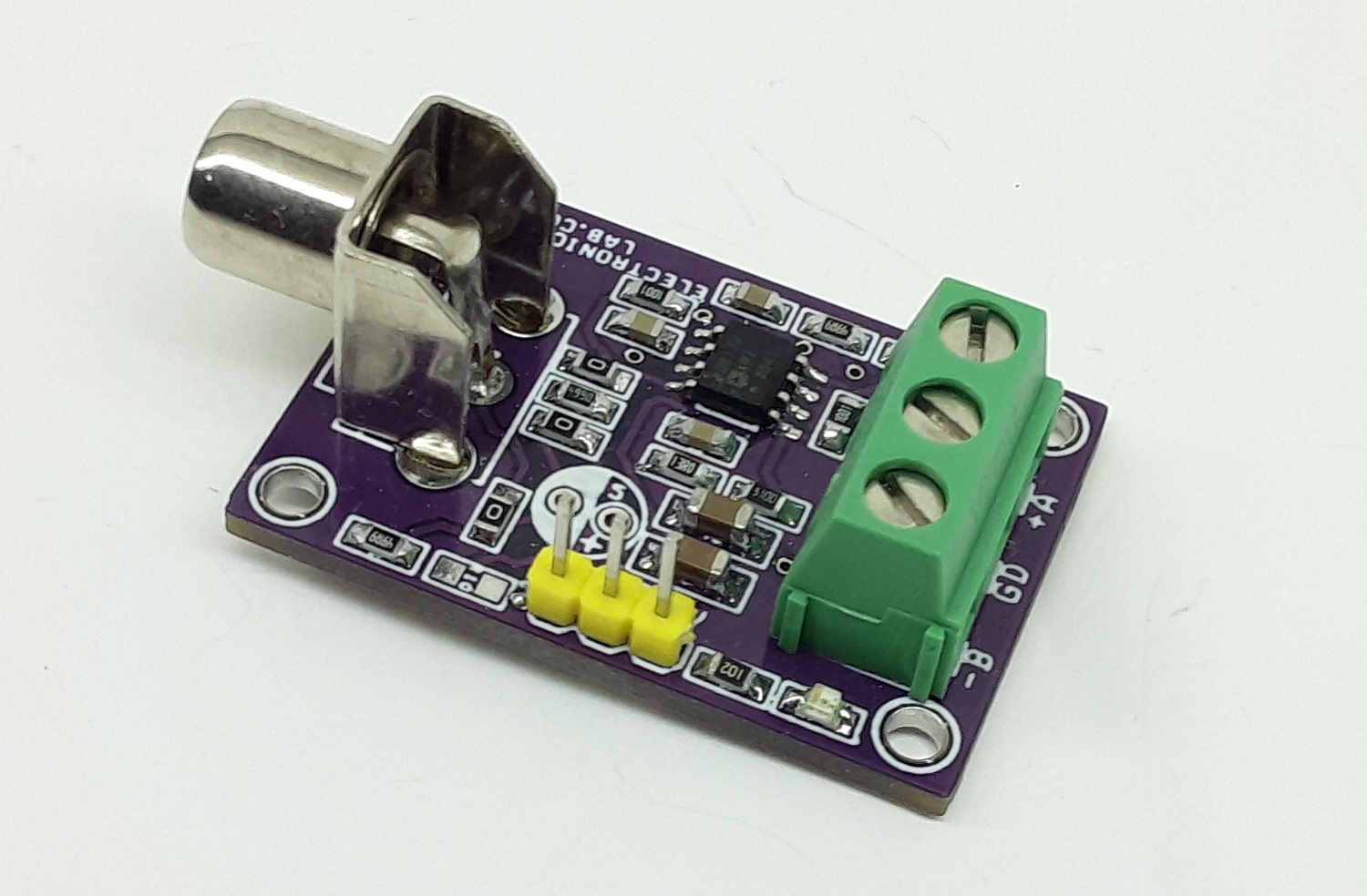
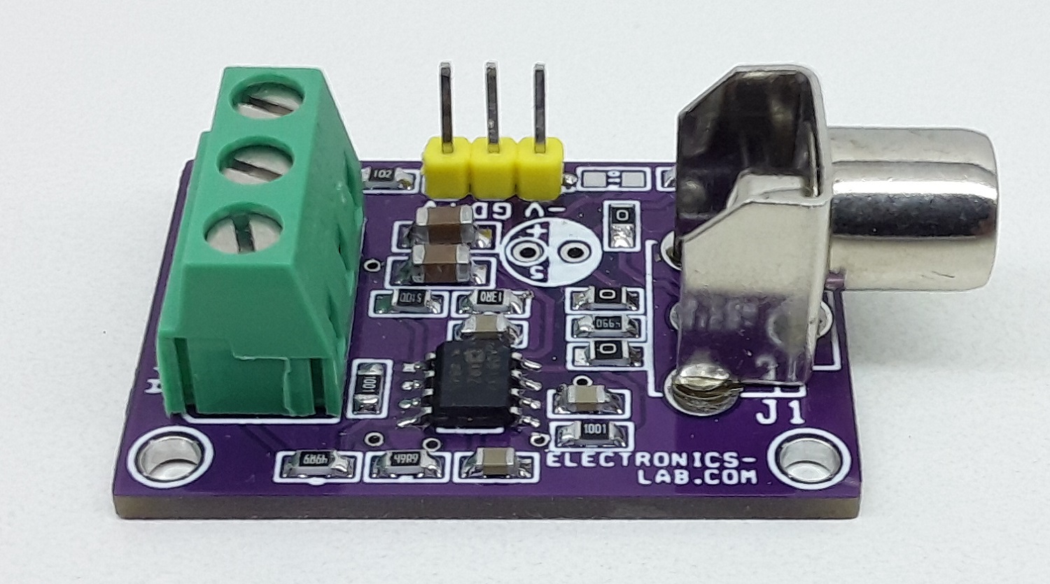
The project presented here is capable of supplying 400mA of current from a 3.7V Li-Ion/Li-Po Battery input with a 5V output. The converter has an internal soft start and internal frequency compensation features. The project is built using LTC3426 SOT23-6 chip. The LTC3426 chip is in a low profile (1mm) SOT-23 package and has a very low shutdown current of about 0.5µA. A switching frequency of 1.2MHz allows a tiny solution. The tiny PCB can be mounted on the backside of the a 18650 battery holder. Jumper J1 is the shut-down jumper. Internal soft-start eases inrush current issues.
The LTC3426 step-up switching regulator generates an output voltage of up to 5.5V from an input voltage as low as 1.6V. Ideal for applications where space is limited, it switches at 1.2MHz, allowing the use of tiny, low cost and low-profile external components. Its internal 2A, 100mΩ NMOS switch provides high efficiency even at heavy load, while the constant frequency, current-mode architecture results in low, predictable output noise that is easy to filter. Anti-ringing circuitry reduces EMI concerns by damping the inductor while in discontinuous mode, and internal soft-start eases inrush current worries. Internal frequency compensation is designed to accommodate ceramic output capacitors, further reducing noise. The device features a very low shutdown current of 0.5µA.
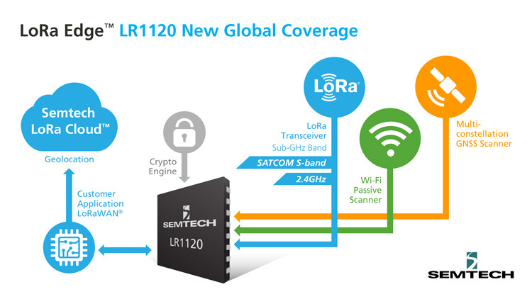
California-based Semtech Corporation, the provider of high-performance analog and mixed-signal semiconductors, will now support worldwide asset tracking on its LoRa Edge Platform. LoRa has been a popular choice for manufacturers for asset tracking in industrial and commercial settings, and Semtech’s LoRa Edge Platform is one example. The new LoRa Edge LR1120 supports direct satellite-connected Internet of Things applications in supply chain management and logistics. The low-power design makes the LR1120 system-on-chip a desired candidate for geolocation on a global scale.
LoRa Edge LR1120 provides multi-band LoRa and Long-Range Frequency Hopping Spread Spectrum (LR-FHSS) communication in a 2.4GHz ISM band and licensed S-band for satellites. It also integrates a Cloud-native multi-constellation global navigation satellite system (GNSS) scanner and a passive Wi-Fi MAC address scanner through the existing LoRa Cloud services. The SoC is designed to meet the physical layer requirements of LoRaWAN specifications while also complying with application-specific demands.
Semtech’s LoRa is targeting track and trace challenges faced by the logistics industry today with a geolocation IoT platform adapted to global transportation and mass-scale asset management,” said Marc Pégulu, vice president of IoT product marketing for Semtech’s Wireless and Sensing Products Group. “With the launch of multi-band LoRa support, coupled with LoRa Cloud services, it has never been easier to expand ubiquitous IoT connectivity and geolocation globally.
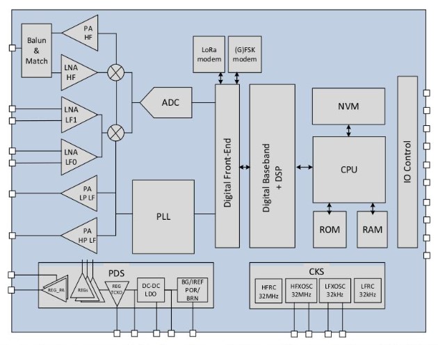
LoRa Edge LR1120 features a low-power, high sensitivity LoRa half-duplex RF transceiver that has a low-noise figure front-end. In terms of the cryptographic engine, the hardware supports AES-128 encryption/decryption-based algorithms and handles device parameters such as DevEUI and JoinEUI. The hardware is claimed to be fully compatible with SX1261/2/8 devices and the LoRaWAN standard.
Combining LoRa with small, relatively low-cost LEO satellites will change the game for LoRa and IoT. Adding satellite communication capabilities in the S-band to LoRa can help replace aging SCADA monitoring and open up new applications and markets, especially in remote regions. So far, LoRa has attracted the interest of several satellite companies including EchoStar and Lacuna, said Christopher Taylor, director, RF & Wireless with Strategy Analytics.
The manufacturer has provided Mouser Electronics’ buy link for the public availability LoRa Edge LR1120, and the pricing for 1x quantity is $187.5 USD.
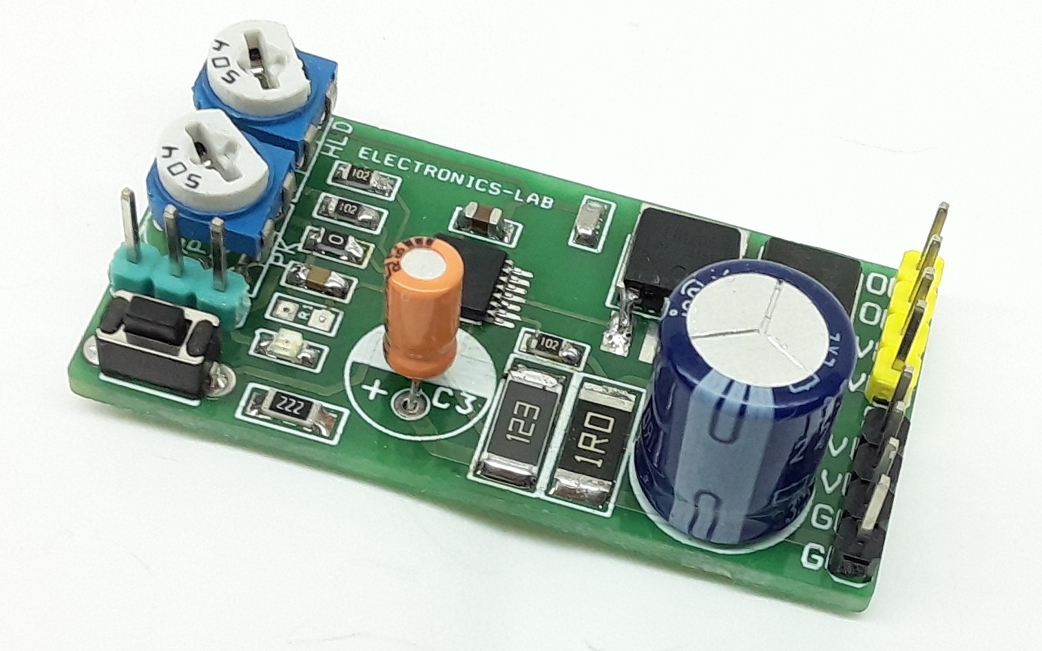
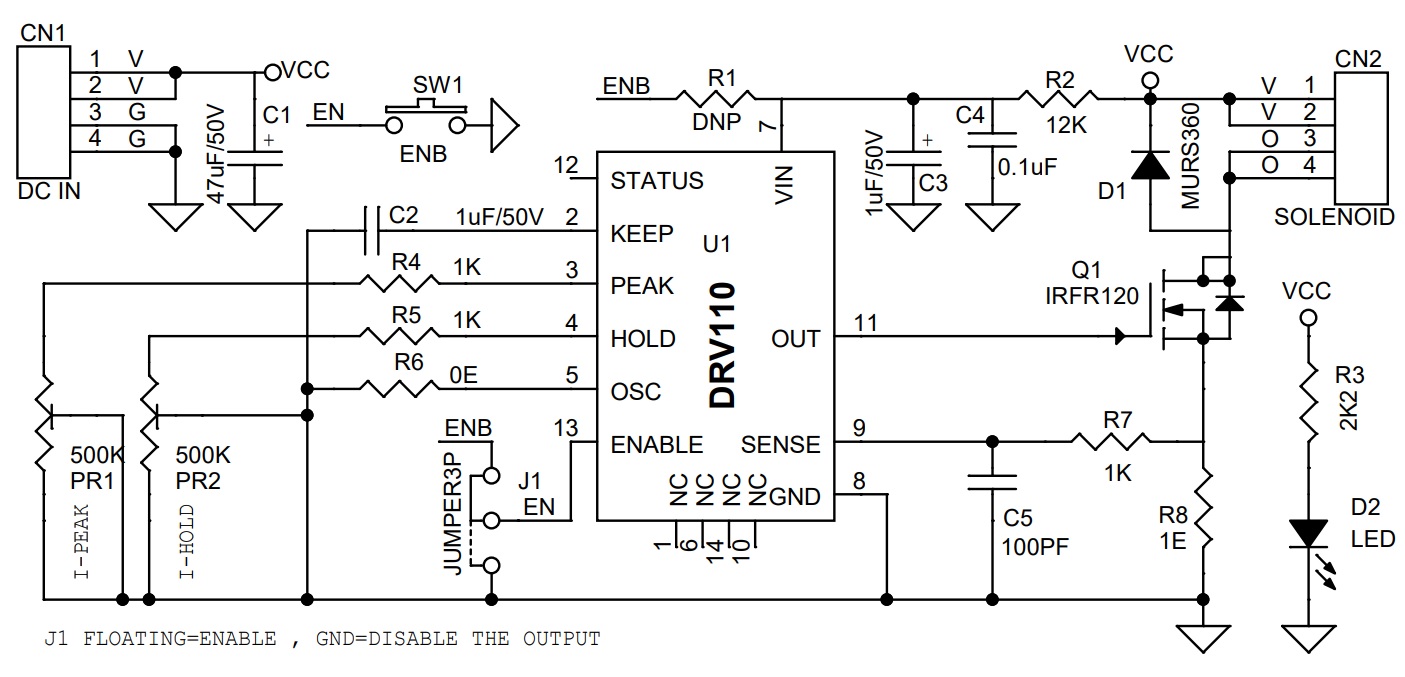
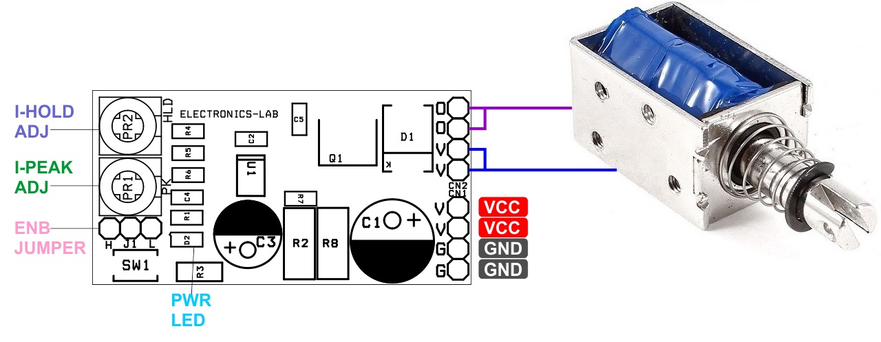
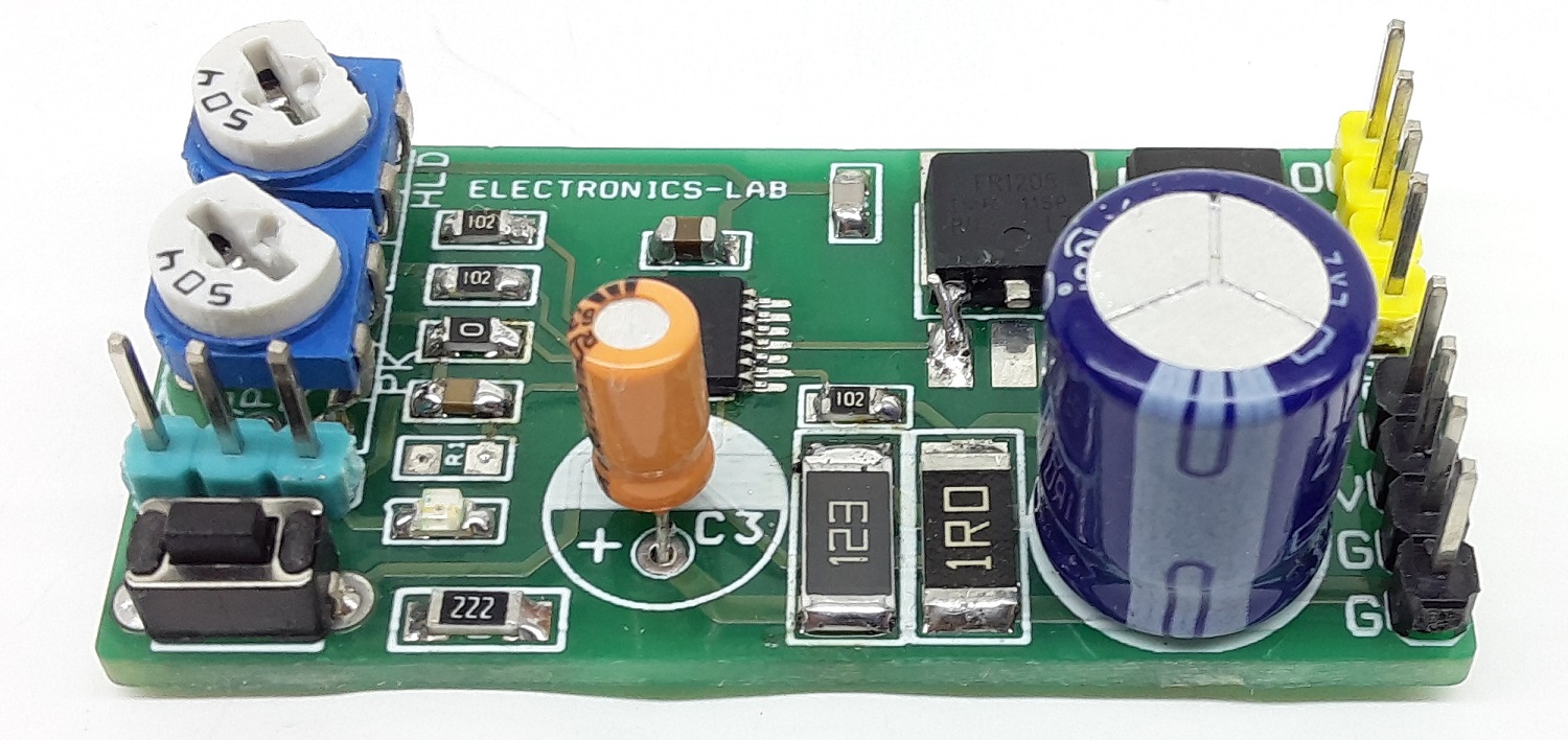
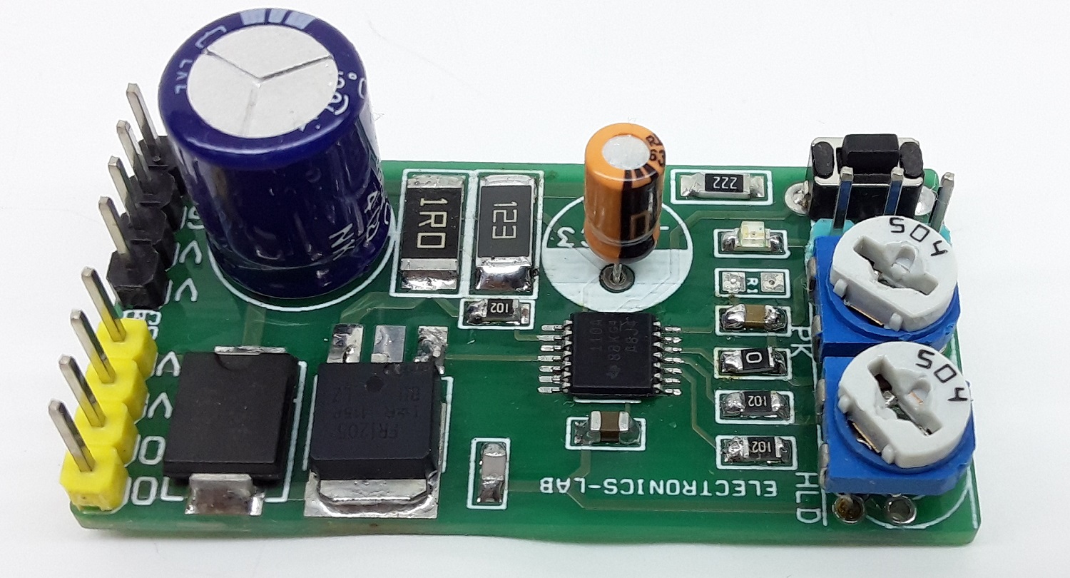
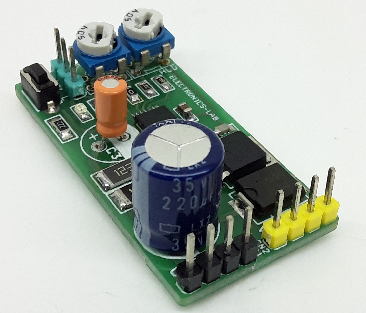
The project described here is a power-saving pulse-width modulator (PWM) controller for solenoids with an internal supply regulator. The board is based on the DRV110 IC which is a PWM current controller which is specifically designed for solenoid and relay applications. The project regulates the current with a well-controlled waveform to reduce power dissipation on the load. The solenoid current is ramped up fast to ensure the opening of the valve or relay. After initial ramping, the solenoid current is kept at a peak value to ensure correct operation, after which the current is reduced to a lower hold level to avoid thermal problems and reduce power dissipation.
Note: The board operates with 24VDC supply, but it can be used with a wide range of power supplies, you may need to calculate resistor value R2, it is advisable to read the datasheet of DRV110 for more information.
Features
Supply 24V DC (Range 15 to 48V DC -> Read Note)
Load Current -> Read Below
Fast Ramp-Up of Solenoid Current to Ensure Activation
Solenoid Current is Reduced in Hold Mode for Lower Power and Thermal Dissipation
IPeak (Peak Current) Adjustable Using Trimmer Pot PR1
IHold (Holding Current) Adjustable Using Trimmer Pot PR2
Jumper J1 Pull Low Disables the Output, pull high or Floating Enables the Output
D2 Power LED
Operating Frequency 20Khz (Can be altered), adjust resistor R6
PCB Dimensions 46.06 x 23.36 mm
Components
D1 Power LED
Q1 MOSFET to drive the Load
D1 Clamp Diode
CN1 power supply input
CN2 solenoid Connections
PR1 peak current adjust
PR2 Hold Current Adjust
Jumper J1 Enable or disable the Output
Resistor R6 Frequency Adjust
Example Application Values when RSense R8 = 1Ohms
Peak Current 150mA When R-Peak (PR1 + R4) = 400Kohms
Holding Current 50mA When R-Hold (PR2 + R5) =200kOhms
Keep Time 100mS When Capacitor C2 = 1uF
PWM Frequency 20Khz
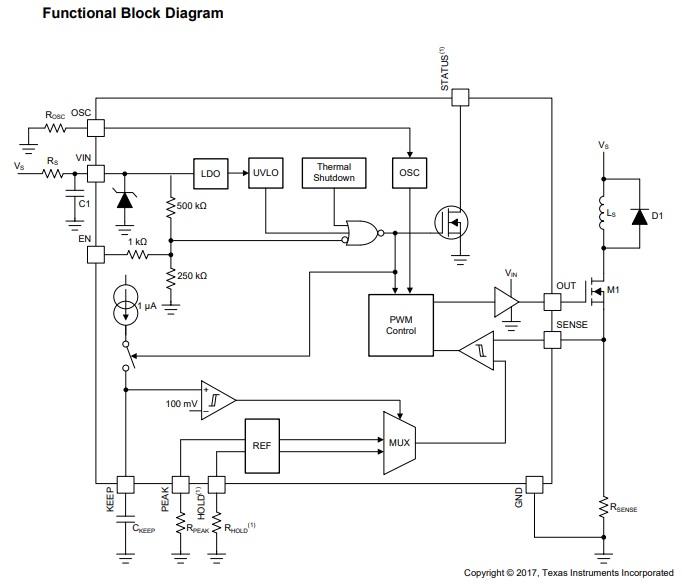
The peak current duration is set with an external capacitor C2. The peak and hold levels of the current ramp can be adjusted using trimmer potentiometer PR2 and PR1, as well as the PWM frequency, which can independently be set with external resistor R6. External setting resistors can also be omitted if the default values for the corresponding parameters are suitable for the application. The DRV110 device has an internal Zener diode that limits the supply at VIN to VZENER for applications that require a higher supply voltage. High DC voltages such as 48V can also be accommodated this way.
Enable Jumper J1
Enable and disable the switch is controlled by the EN pin. The EN pin contains an internal resistor network to set the pin to logic HIGH when the EN pin is floating. This feature can be used for situations where a control signal is not required and the solenoid is only energized when a supply voltage is present. Such applications could be valves or contactors. By pulling down Enable pin disable the output.
Configuring Peak and Hold Currents
IPEAK and IHOLD depend on PR1 and PR2 trimmer pot resistance values RPEAK-PR1 and RHOLD-PR2 as shown in the circuit. If the PEAK pin or HOLD pin is connected to the ground or RPEAK or RHOLD is less than 43.33 kΩ (typical), then IPEAK is at its default value of 300 mA for IPEAK and 50 mA for IHOLD.
The IPEAK value can alternatively be set using trimmer pot PR1. For example, if a PR1 60-kΩ (= RPEAK) is connected between PEAK and GND, and RSENSE = 1 Ω, then the externally set IPEAK level will be 900 mA. If RPEAK -PR1 = 200 kΩ and RSENSE = 1 Ω, then the externally set IPEAK level will be 300 mA. It is not recommended to use a resistor between 30 kΩ and 55 kΩ to avoid the IPEAK or IHOLD current slipping from the maximum current setting to the default setting. In case RSENSE = 2 Ω instead of 1 Ω, then IPEAK = 450 mA (when RPEAK-PR1 = 55 kΩ) and IPEAK = 150 mA (when RPEAK-PR1 = 200 kΩ
Configuring the PWM Frequency Resistor R6 (Default Frequency 20Khz Resistor R6 Value 0 Ohms)
Frequency of the internal PWM clock signal, PWMCLK, that triggers each OUT pin ON-cycle can be adjusted by external resistor R6, ROSC, connected between OSC and GND. Frequency as a function of resistor value is shown in Figure 1. The default frequency is used when OSC is connected to GND directly. Use Equation 1 to calculate the PWM frequency as a function of the external fixed adjustment resistor value (greater than 160 kΩ).
fPWM=60Khz/R6-ROSC x 66.67kOhm; 160Kohm<R6-ROSC<2MOhms
OFF-STATE
OFF state In the OFF state, the EN pin is low and the PWM output is off.
PEAK STATE
The PEAK state begins when the EN pin is set high and ends when the tKEEP time has been reached. During this state, the PWM operates to reach the IPEAK current set by the RPEAK resistor.
Hold STATE
HOLD state In the HOLD state, the tKEEP time has been reached, and the PWM continues to operate but at the IHOLD level. This continues until the EN pin is set low again and the PWM turns off.
SHUTDOWN
The DRV110 turns off the gate driver in Undervoltage lockout (VIN < 4.6 V) or thermal shutdown (TJ > 160°C). If temperature shutdown is activated, the DRV110 resumes operation when the junction temperature is below 140°C.
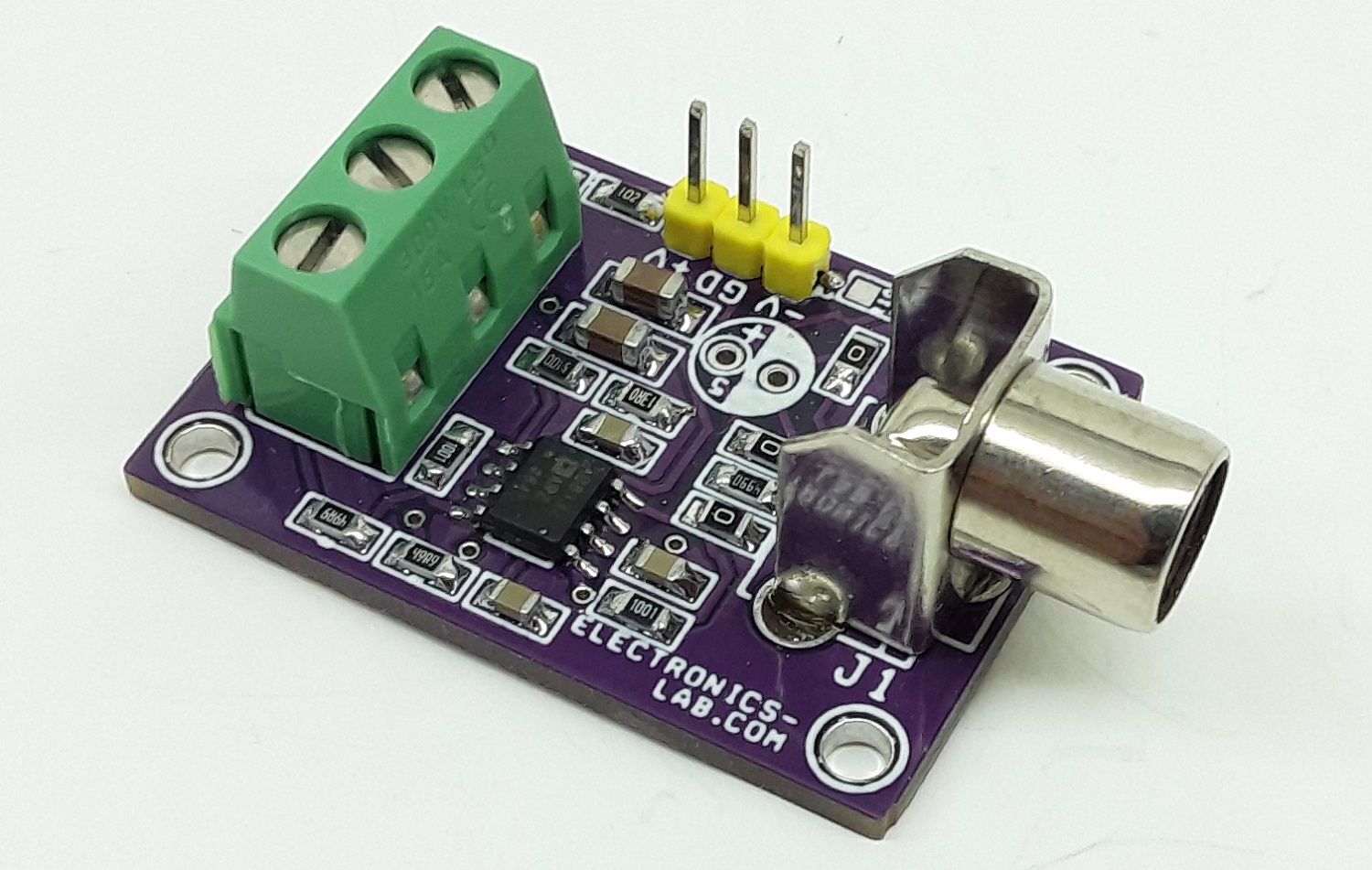
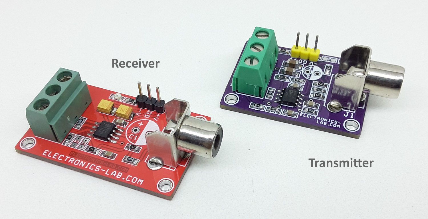
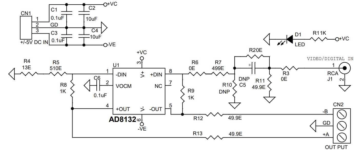
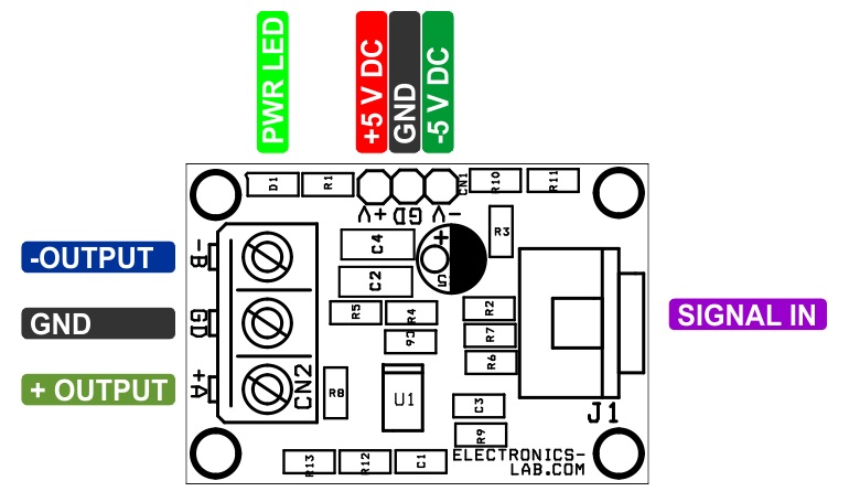
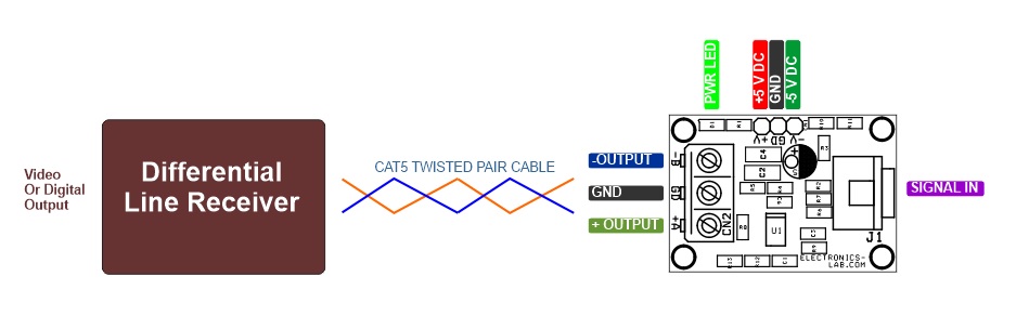
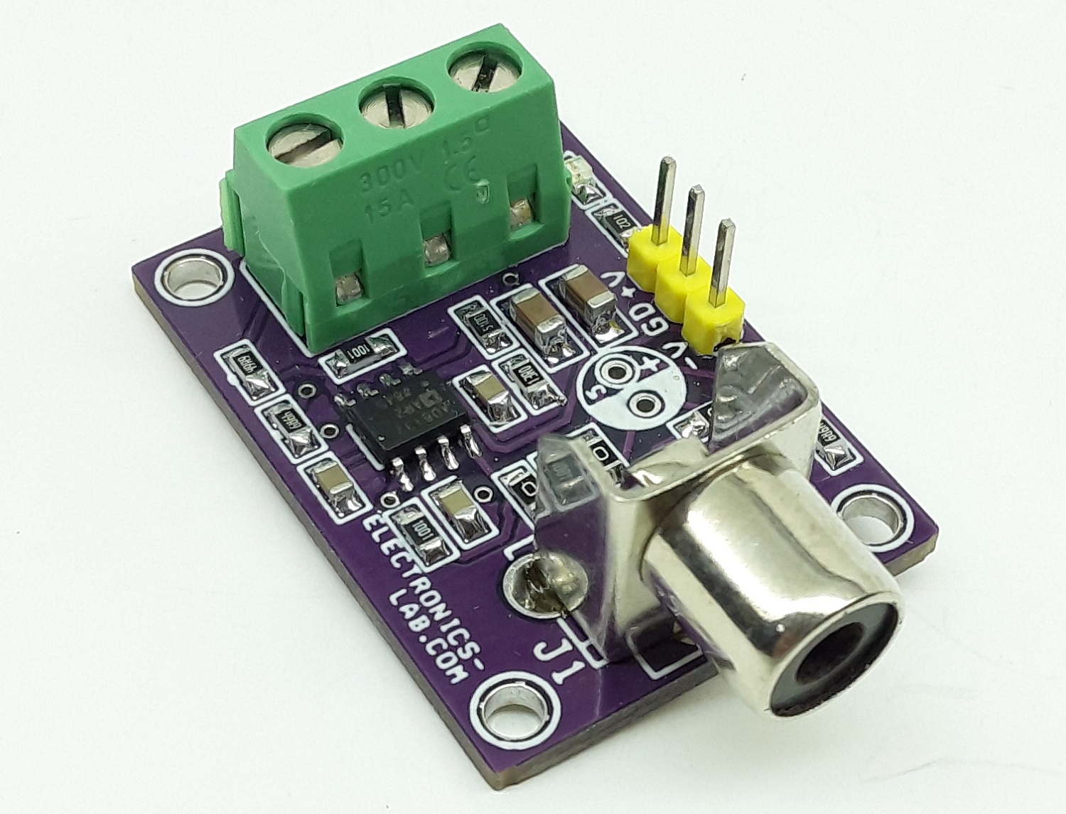
The project presented here is a differential driver for the transmission of high-speed signals over low-cost twisted pair or coaxial cables. The project was built using the AD8132 chip. It can be used to transmit either analog or digital video signals or another high-speed data transmission. The board is capable of driving either a Category 3 or Category 5 twisted pair or coaxial cable with minimal line attenuation. It is capable of operating with a 10 meters of Category 5 cable.
Gain Setting: Default gain is G= +2, refer to the datasheet of AD8132 to learn more about gain settings and gain change. Resistors R4, R5, R8, and R9 are used for gain adjustment.
Features
Power supply +/-5V DC (Range: +2.7 V to ±5.5 V)
Low power: 20 mA @ 5 V
Maximum Output Swing +/-3.6V
High speed 350 MHz, −3 dB bandwidth
1200 V/μs slew rate
Resistor set gain (Resistor R8 and R9) Default Gain G=+2
Internal common-mode feedback
Improved gain and phase balance: −68 dB @ 10 MHz
Separate input to set the common-mode output voltage
Low distortion: −99 dBc SFDR @ 5 MHz, 800 Ω load
PCB Dimensions 36.04 x 25.08 mm
The AD8132 is a low-cost differential or single-ended input to differential output amplifier with resistor set gain. The AD8132 is a major advancement over op amps for driving differential input ADCs or for driving signals over long lines. The AD8132 has a unique internal feedback feature that provides output gain and phase matching balanced to −68 dB at 10 MHz, suppressing harmonics and reducing radiated EMI.
Manufactured using the next-generation of Analog Devices, Inc., XFCB bipolar process, the AD8132 has a −3 dB bandwidth of 350 MHz and delivers a differential signal with −99 dBc SFDR at 5 MHz, despite its low cost. The AD8132 eliminates the need for a transformer with high-performance ADCs, preserving the low frequency and dc information. The common-mode level of the differential output is adjustable by applying a voltage on the VOCM pin, easily level-shifting the input signals for driving single-supply ADCs. Fast overload recovery preserves sampling accuracy.
Differential signal processing reduces the effects of ground noise that plagues ground-referenced systems. The AD8132 can be used for differential signal processing (gain and filtering) throughout a signal chain, easily simplifying the conversion between differential and single-ended components.
Advantages of Balanced Cable Driver
When driving a twisted pair cable, it is desirable to drive only a pure differential signal onto the line. If the signal is purely differential (that is, fully balanced), and the transmission line is twisted and balanced, there is minimum radiation of any signal. The complementary electrical fields are confined mostly to the space between the two twisted conductors and do not significantly radiate out from the cable. The current in the cable creates magnetic fields that radiate to some degree. However, the amount of radiation is mitigated by the twists, because for each twist, the two adjacent twists have an opposite polarity magnetic field. If the twist pitch is tight enough, these small magnetic field loops contain most of the magnetic flux, and the magnetic far-field strength is negligible. Any imbalance in the differential drive signal appears as a common-mode signal on the cable. This is the equivalent of a single wire that is driven with the common-mode signal. In this case, the wire acts as an antenna and radiates. Therefore, to minimize radiation when driving differential twisted pair cables, make sure the differential drive signal is well balanced. The common-mode feedback loop in this project helps to minimize the amount of common-mode voltage at the output and can, therefore, be used to create a well-balanced differential line driver.l
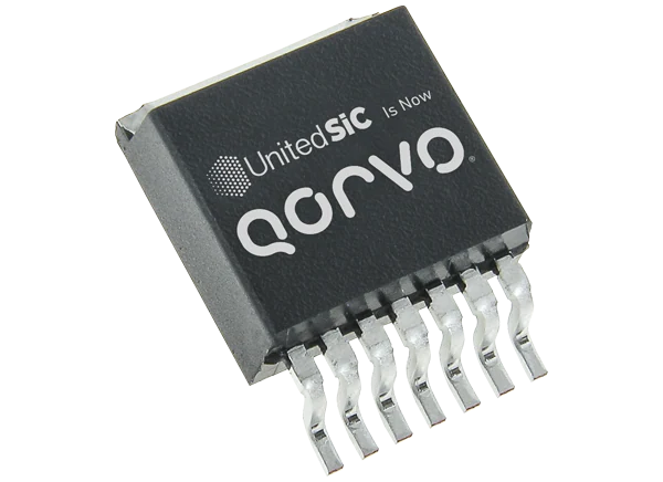
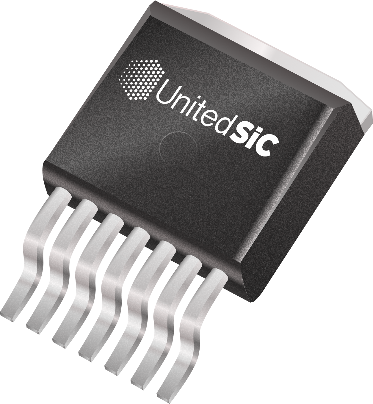
UnitedSiC UF3N170400B7S 1700V-400mW SiC Normally-on JFET exhibits ultra-low on-resistance (RDS(ON)) and gate charge (QG) that allows low conduction and switching loss. The low RDS(ON) value of this JFET at VGS = 0V is ideal for current protection circuits without the need for active control and for cascode operation. The UF3N170400B7S 1700V-400mW SiC Normally-on JFET offers a low gate charge and low intrinsic capacitance. This FET operates at -55°C to +175°C temperature range, is available in a D2PAK-7L package, and is RoHS compliant, halogen-free, and lead-free. Typical applications include over-current protection circuits, DC-AC inverters, switch-mode power supplies, power factor correction modules, motor drives, and induction heating.
Features
Voltage-controlled device
Extremely fast switching not dependent on temperature
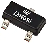
STMicroelectronics’ LM4040 is low power and high accuracy shunt voltage reference providing a stable output voltage over the industrial temperature range (-40°C to +125°C), with a maximum temperature coefficient of 70 ppm/°C. It is available in 0.1%, 0.2%, 0.5%, and 1% initial accuracy versions. The SOT323- 5L and SOT23-3L packages can be designed in applications where saving space is a critical issue. The very low operating current is a key advantage for power restricted designs. The LM4040 is very stable and can be used in a broad range of application conditions.
Features
Fixed 2.048 V, 2.5 V, 3.0 V, 4.096 V, and 5.0 V output voltages
Ultra-low operating current: 10 µA at +25°C
High precision at +25°C: ±0.1% (LM4040A), ±0.2% (LM4040B), ±0.5 % (LM4040C), ±1% (LM4040D)
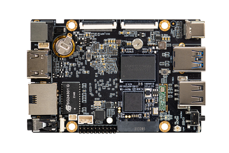
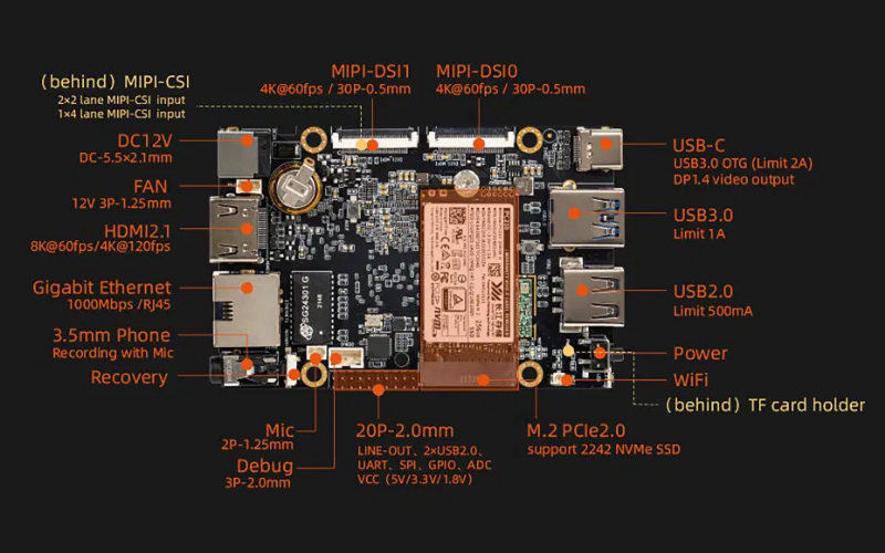
Last year, around this time we saw a credit-card-sized single-board computer from Firefly, built around Rockchip RK3566– ROC-RK3566-PC. In 2022, Firefly released another credit-card form factor single board computer, ROC-RK3588S-PC, powered by a cost-optimized Rockchip RK3588S, an 8-core 64-bit processor for 8K video encoding and decoding. Typically designed for edge computing, artificial intelligence, cloud computing, augmented and virtual reality, and multimedia applications, the mainboard supports up to 32GB RAM and NVMe SSD expansion.
As mentioned earlier, at the heart of the ROC-RK3588S-PC is the next generation AIoT SoC which was unveiled at the Rockchip Developer Event in December 2021 but not many details were available in the public domain. Thanks to CNX-Software, the datasheet for Rockchip RK3588S has been made available highlighting the differences with its original RK3588 high-performance system-on-chip. Some of the differences include the additional HDMI port for video output, which is listed in the datasheet but cannot be seen in the block diagram.
Rockchip RK3588S is a low-power, high-performance processor integrating a quad-core Cortex-A76 and a quad-core Cortex-A55 with a separate NEON coprocessor. The neural network acceleration engine provides processing performance of up to 6 trillion operations per second that support deep learning frameworks such as TensorFlow, Caffe, Tflite, Pytorch, Onnx, NN, Android NN, etc. The graphics engine comes from Arm Mali-G610 supporting high-performance OpenGLES 1.1, 2.0, 3.2, OpenCL 2.2, and Vulkan 1.2, among others.
Evidently specifying the mainboard capable of 8K video encoding and decoding is all possible because of the rich onboard video processing techniques. They support 8K at 60fps H.265/VP9 video decoding and 8K at 30fps H.265/H.264 video encoding which can be done simultaneously. High-quality video processing is possible because of the flexibility to choose from the onboard DRAM which can be up to 32GB, unlike RK3568 which is limited to 8GB. Interestingly, the ROC-RK3588S-PC supports multiple channel input and output with HDMI 2.1 8K video output along with USB-C (DP1.4) and dual MIPI-DSI multi-channel video output allowing up to four-screen video outputs for different displays.
When it comes to wireless connectivity, the board supports 2.4 and 5GHz dual-band Wi-Fi and Bluetooth 4.2 for IoT applications. There also comes an RJ45 Ethernet port capable of 1000Mbps speed of transmission. To increase onboard storage, there is M.2 PCIe2.0 interface that can be connected to a 2242 NVMe SSD storage device, allowing developers to expand storage with TB storage capacity.
More details on the specifications are available on the official product page. The ROC-RK3588S-PC currently sells for $219.00 for 4GB RAM and 32GB storage while the 8GB/64GB module seems to be out of stock at the moment.
In 2017, NVIDIA released the Deep Learning Accelerator (NVDLA), a free and open-source technology designed for embedded and IoT applications. Leveraging the scalability and configurability, NVDLA is integrated into the latest NVIDIA Jetson AGX Orin module that is priced at $1990. In the latest news found in the Linux Kernel mailing list archive, NVIDIA’s Deep Learning Accelerator is proposed to merge driver code into the Linux Kernel for mainline support. The proposal is still in the development phase and would take a while for open-source developers to make substantial contributions.
NVIDIA’s NVDLA comes as a set of IP-core models based on an open standard technology: Verilog model and simulation model in the RTL form, and TLM SystemC simulation model for software development, testing, and system integration. The software stack includes developed infrastructure to convert the existing deep learning models to a form that can be used by the on-device software. This open-source NVDLA hardware and software is made available under the NVIDIA Open NVDLA license and can be accessed via the GitHub repository.
There has been a lot of development around NVIDIA Deep Learning Accelerator technology since its introduction, and back in 2018, SiFive announced the first open-source RISC-V-based SoC platform integrated with the NVDLA. At the Hot Chips conference, SiFive demonstrated the NVDLA running on an FPGA connected via ChipLink to SiFive’s HiFive Unleashed board built around the Freedom U540 Linux-capable RISC-V processor for edge applications.
“NVIDIA open-sourced its NVDLA architecture to drive the adoption of AI,” said Deepu Talla, vice president and general manager of Autonomous Machines at NVIDIA. “Our collaboration with SiFive enables customized AI silicon solutions for emerging applications and markets where the combination of RISC-V and NVDLA will be very attractive.”
Another recent development with NVDLA into a RISC-V-based platform comes from a research article that evaluated the performance of NVDLA by running the YOLOv3 object-detection algorithms.
“We further analyze the performance by showing that sharing the last-level cache with NVDLA can result in up to 1.56x speedup. We then identify that sharing the memory system with the accelerator can result in unpredictable execution time for the real-time tasks running on this platform.”
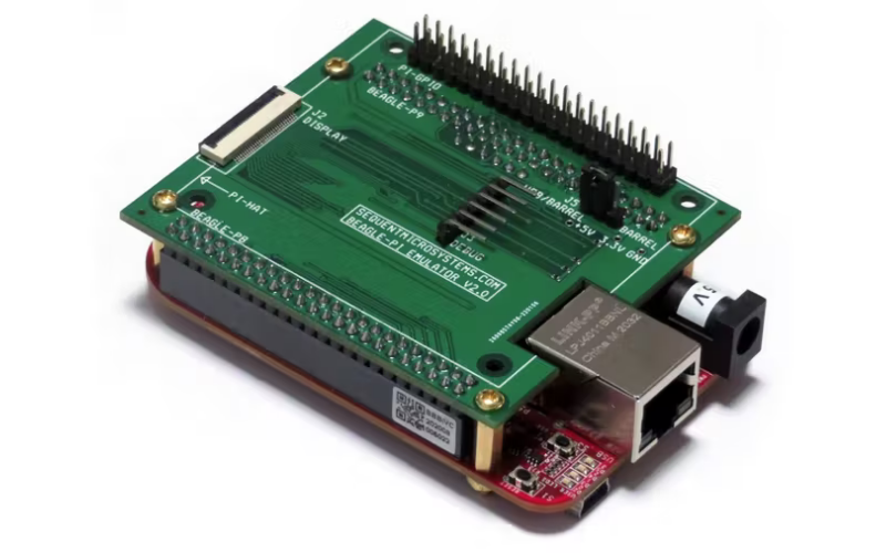
An interesting embedded device created by the Sequent Microsystems, Beagle-Pi, a Raspberry Pi Emulator has solved the problem of incompatibility of HATs to a Beaglebone. The Beagle-Pi converts the two 2 x 23 connectors of the Beaglebone into the 2 x 20 GPIO connector of the Pi making Raspberry Pi HATs compatible with the Beaglebone hardware.
There has been a severe shortage of embedded single-board computers from some of the top manufacturers, including the UK-based Raspberry Pi. The unavailability of these single-board computers resulted in a hike in prices, which are seen as more than 3x the original price while the shipping date of 78 weeks on Mouser for Raspberry Pi 3B. However, the developed ecosystem for Raspberry Pi single-board computers has evolved over time to more than hundreds of HATs. The shortage has limited the use of these HATs that are usually not compatible with most other single-board computers, and certainly not with Beaglebone.
Intro Video
Most importantly, the Beagle-Pi routes all I2C, SPI, and other serial communication GPIOs to the equivalent function pins on the Beaglebone. Also, to mount the Beagle-Pi onto the Beaglebone, four mounting holes– four brass standoffs, screws, and nuts will be shipped along with the hardware depending on the pledge option.
“We tested all the Sequent Microsystems cards run on the Beagle-Pi. The software was compiled without any modifications. You simply download the software from GitHub, compile it on the Beagle and you are ready to go.” Here is our 8-RELAY card to run the self-test program on Beagle:
Replay HAT Video
“Our business is very dependent on Raspberry Pi,” Beffa adds. “We all hope that the current shortage is short lived, the Pi will be back in stock soon at affordable prices and nobody will need the Beagle-Pi. Until then, buy your insurance and try the emulator.”
Bealge-Pi has ended the crowdfunding on Kickstarter that aimed for $1000 but successfully raised $3785 with support from a total of 89 backers on various pledge levels. The basic pledge started at $18 that provided a Beagle-Pi using Beagle Bone Black and four brass standoffs, screws, and nuts. The most recent update came on April 6, 2022, for early-bird supporters, “Backers should have received an email with USPS tracking numbers. All the others will be mailed from China in a few days.”
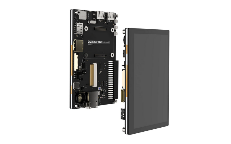
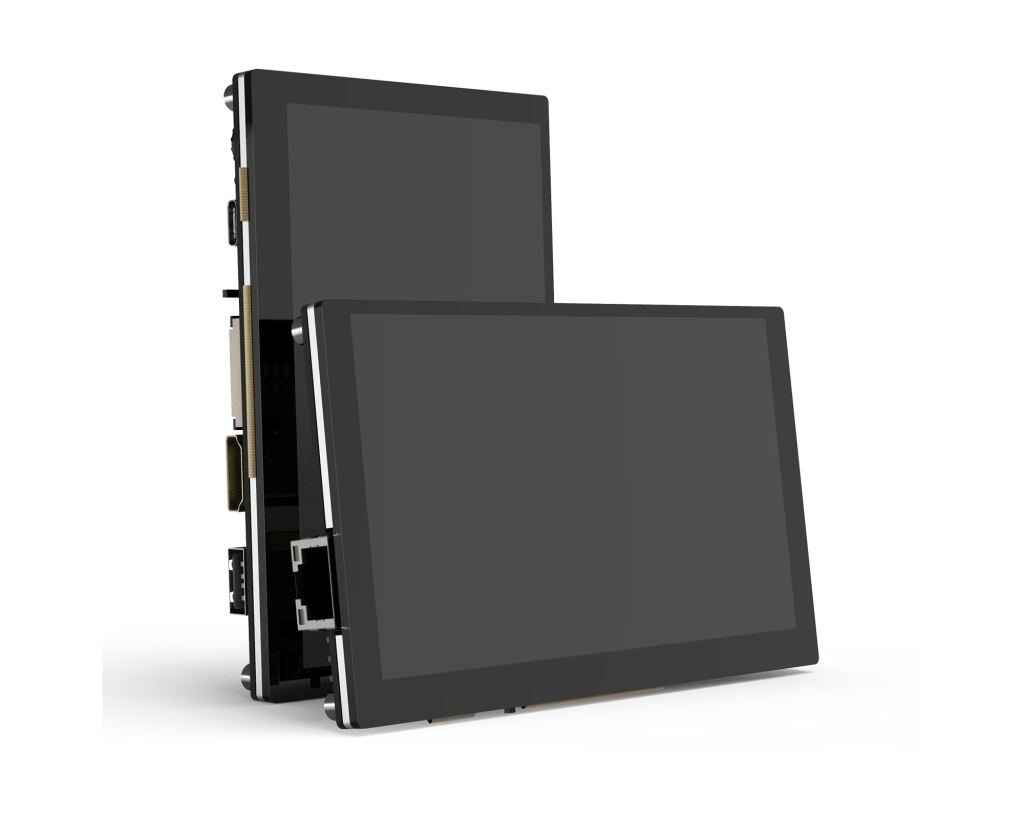
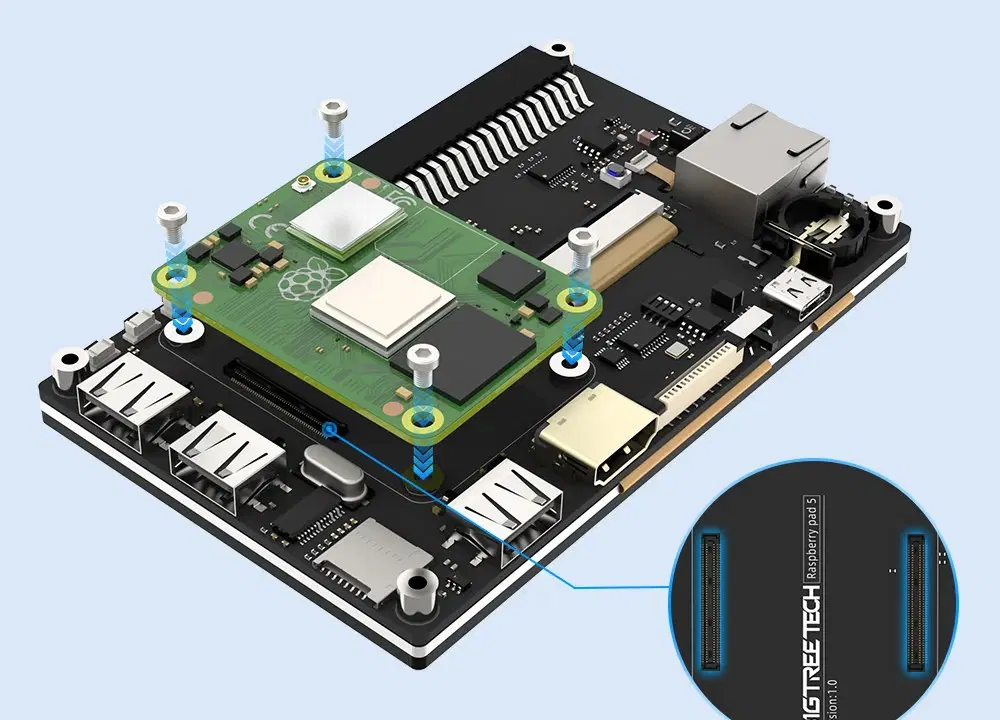
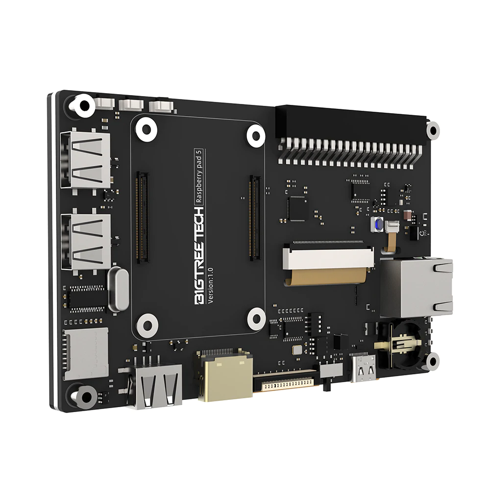
Shenzhen-based 3D printing device manufacturer BIGTREETECH has released the Raspberry Pi Compute Module 4 powered breakout board with an onboard 5-inch IPS touch display screen– named Raspberry Pad 5. Specifically designed for FDM 3D printers, the 5-inch capacitive touchscreen display comes with a resolution of 800×480 pixels and provides a wide viewing angle. Other than 3D printers, the Raspberry Pi CM4-based 5-inch LCD screen can be used for a variety of applications from IoT to industrial automation.
As mentioned earlier, the Raspberry Pad 5 is built around the famous Raspberry Pi Compute Module 4 that incorporates a quad-core Arm Cortex-A72 processor core with dual video output and a wide selection of interfaces. The module is available in 32 variants depending on the RAM and eMMC flash storage options along with wireless connectivity. There has already been a long list of carrier boards that come with Raspberry Pi CM4 and there is a list developed by the developer Jeff Geerling.
Specifications of Raspberry Pad 5
Module: Raspberry Pi Computer Module 4 and Compute Module 4 Lite
Display: 5-inch IPS touch display screen
Resolution: 800×480 pixels HD
Storage: MicroSD card slot for the Raspberry Pi CM4 Lite
Interfaces: HDMI, USB 2.0, CSI port, and USB Type-C
GPIOs: 40-pin
Wireless connectivity: Wi-Fi (on selected models only)
Video transmission: HDMI port
Power supply: 5V via USB Type-C port
Dimensions: 121×75.9 mm
Video
“The Raspberry Pad 5 is an affordable mainboard solution for your 3D printer and other devices. Compatible with the entire series of the Raspberry Pi CM4 board, the device makes for a perfect main control board system. As well as 3D printing applications, it’s also intended for makers to use in a variety of DIY projects.”
Measuring 121×75.9 mm, the LCD screen provides various interfacing options including HDMI, 40-pin GPIO, RJ45 Ethernet port USB Type-C for power, 3x USB 2.0 slots, and a CSI port for camera interfacing. Normally used for video transmission, the HDMI port allows the developer to connect any display of up to 2K resolution. The onboard Type-C port is designed to provide multiple functions such as flashing eMMC storage, CAN bus, and power supply.
Raspberry Pad 5 backside
The Raspberry Pad 5 is currently available for sale for $99.00 (without the Raspberry Pi CM4 module) on the BIGTREETECH product page with various options to choose from. The bundle starts at $165 which includes Wi-Fi wireless connectivity as well.