Foundries.io and Arduino presents Pro Portenta X8 for Secure IoT Solutions

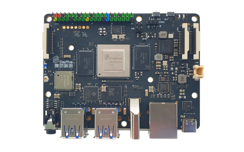
Foundries.io and Arduino announce their partnership to deliver secure, cloud-based embedded Linux IoT and Edge solutions for enterprise with the flagship Arduino Pro Portenta X8 system on module (SoM). Arduino Pro Portenta X8 is an SoM that combines a Linux-based PaaS with docker support to the functionality of a Portenta H7 SoM.

Security factor determines the scalability of the target application for IoT or Edge products, thus an agile infrastructure plays a significant role in making the solution fitter for the industry.

This product enables secure management and maintenance of IoT devices because all the software needed to securely update edge devices is provided through a robust DevOps platform. The IoT and Edge devices market is expected to grow in the next five years. It’s the responsibility of every Linux-based device maker to handle security, testing, and maintenance, but for many this requires they branch out into a completely different field of networking and security.

The solutions for enterprise businesses must handle cyber security of these devices and dedicated infrastructure for maintaining the Linux OS., firmware, and applications. Foundries.io solves these issues through a utility called FoundriesFactory, a cloud-based DevOps service to build, test, deploy, and maintain IoT and edge devices. It accelerates product firmware, OS, and applications development, and provides support for monitoring and incremental Over The Air (OTA) updates of the Linux OS, firmware, and applications of devices and fleets.

Hence, Arduino and Foundries.io, each with their respective expertise, simplified the approach for a ready-to-use solution that can help our customers build IoT and edge systems with confidence. By embedding a FoundriesFactory in the Arduino platform, customers can be sure to choose the best solution on the market.

Portenta X8 top
Arduino Pro Portenta X8

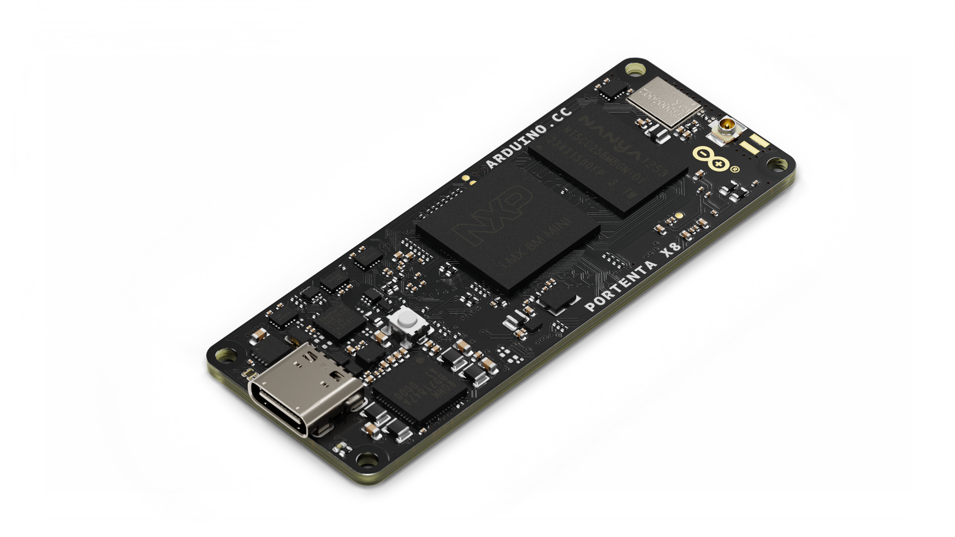
Previously, Arduino pioneered a new product category by integrating microcontrollers and microprocessors on a single hardware platform. Now Arduino Pro Portenta X8 aims to take this experience to the next level by providing the same flexibility to enterprises.

The combination of the Portenta X8 and the FoundriesFactory basically provides a robust microcontroller for IoT edge devices with infrastructure to maintain and secure the underlying Linux OS. Besides, cloud support gives freedom of choice for connectivity to public or private cloud services. Plus, docker container support and orchestration can maintain a whole fleet of edge and IoT devices through FoundriesFactory.

FoundriesFactory is accessible for the Pro Portenta X8 hardware platform. Users can immediately connect Arduino Portenta X8-based products to the cloud and start developing container-based applications through in-built docker support, leveraging device management and DevOps capabilities. Some of the support features provided by FoundriesFactory concerning software development, device management, and OTA maintenance are:

FoundriesFactory Software Support

foundries-tech-stack

The FoundriesFactory service provides many open source projects as a service combined to form a complete software platform. Since individual components are open source, they can be easily customized as per product requirements and add your proprietary IP.

FoundriesFactory implements software engineering concepts of CI (continuous integration) for testing and maintenance of edge devices. The user can store privately source code for different builds using git management. The CI pipeline gets triggered for each commit to building the latest code. It also allows testing on local or remote devices without re-flashing.

Once development is completed, it is easy enough to promote to release through the above CI pipeline. This could enable the user to deploy updates as needed based on the use case, compliance and market requirements.

Apart from this, it has full support for Docker containers (optional) to simplify the orchestration of edge devices and services. Also, the user can customize some of the OS code as per the hardware and application use case.

FoundriesFactory Device/Fleet Management

The user can provision secure devices with individual keys during or post-manufacture to leverage external Hardware Security Modules for secure protocols.

Also, the user can update remote devices and fleets using the Factory CLI or REST API and get secure access to remote devices through a VPN service.

To know more about FoundriesFactory services, please visit this link.

FoundriesFactory – OTA Update Feature ArchitectureOTA Architecture

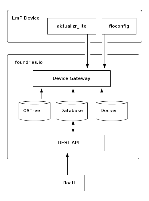
Edge devices communicate with the device gateway using mutual TLS. The device gateway provides a set of REST APIs to support aktualizr-lite, fioconfig and docker authentication.

Aktualizr-lite and fioconfig run as separate daemons that periodically poll the device gateway with HTTP GET requests on configurable intervals. Due to the fact devices are polling the server, REST API changes requested by fioctl happen asynchronously.

Aktualizr-lite validates available targets that a device may install. The algorithm followed for OTA updates on edge devices is:

  1. Check for new root.json. This allows a device to know about key rotations before going further.
  2. Request for timestamp.json metadata.
  3. Request for the snapshot.json metadata.
  4. Ask for the targets.json metadata.

At this point, the device will have all the details regarding new updates and install the latest target build accordingly.

This explains all about Arduino Pro Portenta X8 and FoundriesFactory integration to deliver enterprise-ready cloud-based Linux solutions to secure and maintain hardware OS.

Doogee S98 Set To Launch On March 28th With A Fresh New Look And A Maasive Discount

The new S98 rugged phone was announced last week by Doogee. The company will launch the rugged phone next month on AliExpress and Doogemall (the company’s official shopping platform).

To recap the features of the Doogee S98. Firstly, it comes with a round rear display. The second display looks like a smartwatch completed with stylish bezels. The display also allows a great level of customization by users. Uses include controlling music, checking the time, battery level, and keeping up with notifications among others.

Also on the back of the phone is a Triple camera setup, the main 64MP main, an 8MP wide-angle camera, and the most interesting of the set, a 20MP night vision camera. The night vision camera allows you to capture and record videos in pitch-black environments. Thanks to the infrared light on the side, a clear picture is almost always guaranteed.

Under the hood, MediaTek helio G96 runs the show. The octa-core processor is designed for gaming which means faster performance.

Doogee S98 – | Gaming performance test | Antutu benchmark score |

The battery on this beast is a 6000mAh battery capable of carrying you 2-3 days of active use depending on your usage behavior. It comes with a 33W fast charger and supports a 15W wireless charger.

The main screen is a 6.3” FHD+ corning gorilla glass-protected display. It will run Android 12 out of the box which brings a host of advantages on the security and optimization front. It also comes with a fingerprint scanner and a custom button on either side of the phone. The features are completed with NFC, 4 navigational satellite support, toolkit, custom button, side mounted fingerprint scanner and many more

Not to forget, S98 is waterproof, drop-proof, and can withstand extreme weather.

Doogee S98’s global launch has been booked for March 28. Between March 28th and April 1st, it will be at its lowest price. We will keep you updated when Doogee reveals the price. But, if you want a free S98, Doogee is giving away 8 of them. To throw your hat in the ring, check the official S98 page for more details on the giveaway.

Win a Digilent Analog Discovery Pro 3000 ADP3450

Enter for free…

This month oemsecrets.com has partnered with Digilent to give away an Analog Discovery Pro ADP3450 worth $1295. To enter simply follow the link below for your chance to win.

Get additional entries into the giveaway by sharing this link on Instagram, LinkedIn, Facebook or Twitter using #oemsecrets or @oemsecrets or by following us on LinkedIn.
ENTER FOR FREE

About the Analog Discovery Pro ADP3450

The ADP3450 is the first in the line of Analog Discovery Pro devices and take the analog and digital instruments from the internationally popular Analog Discovery and turn up key functionalities to meet the growing need for professional-level home electronics test benches…read more

Terms and Conditions

This competition is managed and hosted by OEMSECRETS LIMITED, where the precondition for competition entry, for a chance to win an Analog Discovery Pro 3000 ADP3450  is an email subscription to the oemsecrets.com mailing list. This includes the latest electronics industry updates, offers, and product news from OEMSECRETS LIMITED. Subscribers can change preferences or unsubscribe at any time using the links in the footer of any email sent to you from OEMSECRETS LIMITED. The competition closes on 29th April 2022 at 11.59 BST. The winners will be announced the following week via email and on social media. We will contact the winners by email and request shipping information to send the product via UPS tracked shipment and paid for by us worldwide. If we do not hear back via email after two attempts of making contact within 14 days, the prize will be forfeited and a new winner will be chosen.

Audio Line Receiver using INA134

The project described here is a differential line receiver consisting of high-performance INA134 OPAMPs with on-chip precision resistors. The project is fully specified for high-performance audio applications and has excellent AC specifications, including low distortion (0.0005% at 1kHz) and high slew rate (14V/µs), assuring good dynamic response. In addition, wide output voltage swing and high output drive capability allow use in a wide variety of demanding applications. The INA134 on-chip resistors are laser trimmed for accurate gain and optimum common-mode rejection. Furthermore, excellent TCR tracking of the resistors maintains gain accuracy and common-mode rejection over temperature. Operating power supply ±4V to ±18V (8V to 36V total supply).

Audio Line Receiver using INA134 – [Link]

Audio Line Driver using DRV135 with Balanced Output

The project presented here is a differential output amplifier that converts a single-ended audio signal input to a balanced output pair. This balanced audio project consists of high-performance OPAMPS with on-chip precision resistors. They are fully specified for high-performance audio applications and have excellent AC specifications, including low distortion (0.0005% at 1 kHz) and high slew rate (15 V/µs). The board is based on DRV135 from Texas Instruments.

Audio Line Driver using DRV135 with Balanced Output – [Link]

SparkFun Join Hands With MikroElektronika to design new electronic embedded products

MIKROE x SparkFun Partnership

Serbian electronics embedded manufacturer MikroElektronika is known for releasing one product every day, has now been selected by SparkFun under a new partnership agreement to add new products from the MIKRO ecosystem to the SparkFun e-store. The collaboration will also see fresh products being developed, starting with two new SparkFun Originals with mikroBUS sockets that can interact with Qwiic connect system and MicroMod. SparkFun MicroMod mikroBUS carrier board leverages the onboard Raspberry Pi’s in-house silicon tapeout RP2040 microcontroller and is designed for the Feather board form factor, including a microSD card slot and a JST single-cell battery connector. The other product is a SparkFun MicroMod mikroBUS carrier board with a MicroMod M.2 socket and microBUS 8-pin header that provides a greater degree of freedom to interface with any processor board in the MicroMod ecosystem as well as any Click board in the microBUS ecosystem.

Coming back to the key highlight of SparkFun RP2040 mikroBUS development board priced at $14.95 is integrated with 16MB of flash memory and a programmable WS2812 RGB LED. The onboard RP2040 microcontroller features two Arm Cortex-M0+ processors clocked up to a frequency of 133MHz and incorporates 264kB of embedded SRAM in six banks, 6x dedicated IOs for SPI flash memory, 30x multifunctional GPIOs for dedicated hardware, programmable IOs, and 4x 12-bit ADC channels. However, the Feather form factor board only gets 18x multifunctional GPIO pins divided as up to 2x UART, I2C and SPI buses, up to 8x 2-channel PWM and 4x 12-bit ADC channels with an internal temperature sensor (500kSa/s). On the software side, the RP2040 microcontroller supports both C/C++ and MicroPython cross-platform development environments including easy access to runtime debugging.

SparkFun RP2040 mikroBUS Development Board

To power the SparkFun RP2040 mikroBUS development board, the board is designed with a USB Type-C connector and supports a 2-pin JST connector for a LiPo battery of 500mA charging circuit. For the enhanced user interface, the hardware gets 4x LEDs, like red for the 3V3 power indicator, yellow for battery charging indicator, blue for status/test (GPIO 25), and an addressable RGB LED on GPIO 8. Interfacing external modules and sensors can be done through Qwiic connector and mikroBUS socket, which are some of the universal connectors combining hundreds of external sensors. As an open-source project, the manufacturer has provided Schematic and Eagle PCB design files along with board dimensions and hookup guides.

Another important launch is the SparkFun MicroMod mikroBUS carrier board that takes advantage of three connectors, MicroMod, Qwiic, and mikroBUS for faster prototype reducing time to market. The mikroBUS 8-pin female header with standard pin configuration consists of 3x groups of serial communication pins, SPI, UART, and I2C, while 6x additional pins such as PWM, interrupt, analog input, reset, and chip select, along with 2x power groups of 3V3 and 5V. To charge the single-cell LiPo battery, the carrier board is equipped with MCP73831 single-cell Lithium-Ion/Lithium-Polymer charger IC, while still supporting onboard USB Type-C connector.

Analysis

In the pool of several RP2040 powered development boards, the $14.95 SparkFun RP2040 mikroBUS development board comes with good documentation for newbies. If you are new to RP2040 microcontroller development, the hardware can be a good starting point for the listed price point. The carrier board is no special other than the support for all three MicroMod, Qwiic, and mikroBUS ecosystems while shipping at $19.95. Let us know in the comments if you would buy one, and if so why.

A novel approach for in-pixel processing for resource-constrained edge AI applications

Computer Vision Applications

Computer vision applications that range from object detection and pattern recognition to computational healthcare and security surveillance systems take the input image for further processing, which in traditional hardware implementation has a vision sensing and vision processing platform as a separate entity within the AI system. The segregation of CMOS-based vision sensor platforms and vision computing platform have raised concerns regarding throughput, bandwidth and energy efficiency. To mitigate these challenges, existing research work shows the design approach to bring visual data processing closer to the source, which means closer to the CMOS image sensors through three techniques of near-sensor processing, in-sensor processing and in-pixel processing.

In the proposed near-sensor processing technique, the ML accelerator on the same PCB as the CMOS image sensor chip brings the computation closer to the source but suffers data transfer costs between the processing chip and image sensor. While in-sensor processing solves this bottleneck, they still require data to be real in parallel through communication buses from image sensor photo-diode arrays into peripheral processing circuits. The third approach of in-pixel processing has aimed to embed all the processing capabilities in the image sensor pixels.

Existing and Proposed Solution for Vision Data Processing
Comparison of existing visual data processing and custom P2M techniques

The initial work carried out on in-pixel processing focused on in-pixel analog convolution that required the use of non-volatile memories. This fails to support multi-bit, multi-channel convolution operations required by advanced deep learning applications. As in-pixel processing is relevant to the research paper titled, “P2M: A Processing-in-Pixel-in-Memory Paradigm for Resource-Constrained TinyML Applications” that proposes a novel processing in-pixel-in-memory (P2M) model wherein the memory-embedded pixels will be capable of carrying out massively parallel dot product accelerations using photodiode current as input activation and weights calculations within individual pixels.

Processing-in-Pixel-in-Memory Paradigm

A team of researchers affiliated with the Department of Electrical and Computer Engineering and the Information Sciences Institute at the University of Southern California, United States continued the work to develop a compact MobileNet-V2-based model for P2M hardware implementation on visual wake words dataset (VWW) achieving a reduction of data transfer bandwidth from the sensor to ADCs by up to 21x compared to the standard near-sensor and in-sensor processing implementations.

Processing-in-pixel-in-memory paradigm
Proposed Circuit Technique for processing-in-pixel-in-memory for computer vision applications deployed on resource-constrained TinyML devices

The proposed circuit model has three phases of operation: Reset phase, multi-pixel convolution phase, and ReLU operation. In the first reset phase, the voltage on the photodiode node M is precharged or reset by activating the reset transistor Gr. Next, in the multi-pixel convolution phase, the discharge of reset transistor Gr takes place which deactivates the Gr. Using the select control lines, the gate of the GH transistor is pulled high to VDD to activate the XxYx3 multi-pixels.

“As the photodiode is sensitive to the incident light, photo-current is generated as light shines upon the diode (for a duration equal to exposure time), and voltage on the gate of Gs is modulated in accordance to the photodiode current that is proportional to the intensity of incident light,” the team explains. “The pixel output voltage is a function of the incident light (voltage on node M) and the driving strength of the activated weight transistor within each pixel.”

The pixel output from multiple pixels is taken from the column lines and represented in the multi-pixel analog convolution output. This analog output is converted to digital value through SS-ADC in the periphery circuit and the whole operation is repeated twice for positive and negative weights. Finally, in the ReLU operation, the output of the counter is latched and represents a quantized ReLU output. The entire P2M circuit was simulated using commercial 22nm GlobalFoundry FD-SOI process technology.

Will Processing-in-Pixel-in-Memory be the future?

When most of the low power edge IoT devices have limited on-memory of a few kilo-bytes, the team has implemented a P2M approach on these devices for TinyML applications. Utilizing Visual Wake Words (VWW) dataset comes with high-resolution images that include visual cues to wake up AI-powered home assistant devices requiring real0time interference in a resource-constrained environment. The constraints are defined as the detection of the presence of a human in the image frame with peak RAM close to 250kB for which the input image undergoes downsampling to obtain a 224×224 resolution image. The chosen CNN architecture, MobileNetV2 has 32 and 320 channels for the first and last convolutional layers respectively that support a full resolution of 560×560 pixels. “In order to avoid overfitting to only two classes in the VWW dataset, we decrease the number of channels in the last depthwise separable convolutional block by 3×,” as the team reports.

(Top) Test accuracies custom P2M model against baseline CNN architecture and (Bottom) Performance Comparison against state-of-the-art methods

The entire experimentation of training the baseline and P2M models in PyTorch using an SGC optimizer with 0.9 momentum for 100 epochs is performed on an NVIDIA 2080Ti GPU with 11GB memory. According to the results, as the image resolution increases from 115×115 to 225×225 and then 560×560 pixels, the test accuracy for the custom P2M models improves from 80.00% to 84.30% and then 89.90% respectively. Also, the performance comparison of the proposed P2M models with state-of-the-art deep convolutional neural networks on the VWW dataset shows the method to outperform most of the proposed ideas and is close to the one proposed by Saha et. al. [2].

The research work was published on Cornell University’s research sharing platform, arXiv under open access terms.

References

  1. Gourav Datta, Souvik Kundu, Zihan Yin, Ravi Teja Lakkireddy, Joe Mathai, Ajey Jacob, Peter A. Beerel, Akhilesh R. Jaiswal: P2M: A Processing-in-Pixel-in-Memory Paradigm for Resource-Constrained TinyML Applications. DOI arXiv: 2203.04737 [cs.LG].
  2. Saha, O., Kusupati, A., Simhadri, H. V., Varma, M. & Jain, P. RNNPool: Efficient non-linear pooling for RAM constrained inference. In Larochelle, H., Ranzato, M., Hadsell, R., Balcan, M. F. & Lin, H. (eds.) Advances in Neural Information Processing Systems, vol. 33, 20473–20484 (Curran Associates, Inc., 2020).

HC32L110 is possible the world’s smallest MCU housed in a CSP16 Package

HC32

HDSC HC32L110 is an Arm Cortex-M0+ microcontroller available in a minuscule 1.59 x 1.436 mm CSP16 package, possibly making it the world’s smallest Arm MCU.

HC32L110 Specifications

HC32L110 has an MCU core of Arm Cortex-M0+ 32-bit core up to 32 MHz, 2 to 4KB RAM with parity check, 16K to 32KB flash memory storage with erasing and write protection. Some of the peripherals provided are 16x GPIOs with 20-pin packages, 12x GPIOs with 16-pin packages. It comes with a wide range of peripheral provisions including 2x UART, 1x SPI and 1x I2C PWM output, thus ideal for multi-component systems. Some additional features for the users are the buzzer frequency generator and general-purpose timers and counters.

Talking more about the timers and counters, it comes with 3x general-purpose 16-bit and 1x programmable 16-bit registers dedicated for the timers and counters. The hardware supports 3 timers/counters for high-performance computational counting/timing and 1 low-power counter/timer.

It has an external high-speed crystal oscillator with a frequency range 4 ~ 32MHz, an external low-speed crystal oscillator with a frequency 32.768KHz, an internal high-speed clock with a frequency 4/8/16/22.12/24MHz, and an internal low-speed clock of frequency 32.8/38.4KHz. Watchdog timer and Hardware supports internal and external clock calibration and monitoring.

It is secured by CRC-16 module, a unique 10-byte ID number. For debugging, it has an embedded debugging solution providing a full-featured real-time debugger. The operating voltage for the chip is between 1.8 to 5.5V. It has an Integrated low voltage detector LVD, configurable 16-level comparison level.

Deeper Look at Power Consumption and Modes

The HC32L110 Arm-Cortex M0+ has many different modes with varying power consumption levels:

  • Deep sleep mode (all clocks off, power-on reset valid, IO status maintained, IO interrupt valid) with power consumption at 0.5μA at 3V
  • Deep sleep mode + RTC operation at a power consumption of 1.0μA at 3V
  • Low-speed active mode (CPU and peripheral modules run, run programs from flash) at a power consumption of 6μA at 32.768KHz
  • Sleep mode (CPU stops working, peripheral modules run, the main clock runs) with power consumption at 20μA/MHz @ 3V @ 16MHz
  • Active (CPU and peripheral modules run, run programs from flash) with power consumption at 120μA/MHz at 3V at 16MHz

It works in a temperature range of -40 to 85 degrees celsius with a 4μS wake-up time.

For more details on HC32L110B6YA Arm Cortex microcontroller, please visit this link.

StarFive VisionFive V1 RISC-V Single Board Computer on sale for $179

StarFive VisionFive V1 RISC-V Single Board Computer

After the hype around BeagleBoard Foundation’s BeagleV StarFive RISC-V SBC, the cancellation came as a shock to the embedded developers’ space. However, as an alternative to the original RISC-V single-board computer and continuing most of its features, StarFive unveiled the VisionFive V1 late last year— now available for purchase on ALLNET China. The hardware comes with SiFive’s U74 64-bit RISC-V processor core which is comparable to the Arm Cortex-A55 processor.

At the heart of the single-board computer is the StarFive JH7100 system-on-chip tightly integrated with a dual-core RV64GC ISA U74 high-performance RISC-V application processor clocked at a frequency of 1.0GHz, capable of supporting a fully-featured operating system such as Linux. The SoC comes with Vision DSP Tensilica-VP6 for computing vision at 600MHz (VPU), an NVIDIA Deep Learning Accelerator, and a neural network engine. Incorporating 8GB of LPDDR4 memory, but no onboard storage, however, the manufacturer provides a MicroSD card slot. Even the LPDDR4 memory is divided into 2x 4GB clocked at 2800MHz, which restricts performance, unlike the totally integrated 8GB SDRAM.

Of course, with all the Neural Network Engine, NVLDA Engine and DSP, the board is a powerful piece of hardware for human-machine interface, smart home tech, surveillance, NAS, and even multimedia applications. The board comes with H.264/H.265 video decoder supporting up to 4Kp60 and dual-stream decoding up to 4Kp30 making it one of the most affordable choices for live streaming multimedia implementations.

StarFive VisionFive V1 SBC

It is very important to support various wireless connectivity protocols to take the benefit of the vision processing unit and neural network engine as most of the applications are deployed at the edge. To assist with such projects, the single board computer comes with 2.4GHz Wi-Fi IEEE802.11b/g/n and Bluetooth 4.2 (BLE) wireless connectivity. Also, the onboard Gigabit Ethernet port lets the user share the mobile data connection with the VisionFive V1 SBC over the wired network connection.

On the software side, as mentioned earlier, the hardware is capable of running the Linux operating system with software compatibility for U-Boot Bootloader, GRUB2 Bootloader, Linux Kernel, OpenEuler, Fedora, OpenSBI Firmware. As of writing, the VisionFive V1 RISC-V Single Board Computer starter kit is available for purchase at $179.00 which includes the StarFive VisionFive V1 SBC, Heatsink with fan, and a 32GB SD card with pre-flashed Fedora OS.

Analysis

The hype around BeagleBoard Foundation’s BeagleV StarFive RISC-V SBC explains the demand for StarFive VisionFive V1 SBC due to its powerful system-on-chip and improved functionalities for most hobbyist and industrial projects. The board is seen as a general-purpose SBC reducing its capability to be exploited for one domain, like vision processing. Even though the hardware supports H264 and H265 video decoder, for live video streaming, the hardware requires more memory to process. SDRAM is split into 2 4x RAM, which limits performance and might not sustain processing for high video graphics.

Cat M1 vs Cat 1 vs Cat 4: Connectivity for Telematics

Through increased adoption of data-driven telematics use cases in vehicles, there has been a rising need for telematics edge hardware across a range of vehicles. Telematics and connected vehicle solutions help unlock value across a range of vehicle types: passenger cars, heavy duty trucks, electric vehicles, boats, with the list growing day by day.

Different applications require different data processing and connectivity architectures – A few applications require more edge processing with intelligence on the device, while a few use cases require all data to pushed on to the cloud platforms to build on the analytics and dashboards.

The improvement in the connectivity landscape has enabled vehicles to be connected to the internet. Cellular technology is available from Cat 0 to Cat 19, however, the technology most suited and commonly used in telematics and connected mobility solutions are Cat M1, Cat 1 and Cat 4. A more detailed insight into these 3 connectivity technologies is given below.

A Comparison of throughput: Cat M1 vs Cat 1 vs Cat 4

Cat M1, which also goes by the name LTE Cat M1 originally was designed specifically for IoT Solutions, with an average upload and download speed of 375 kbps. There is a trade-off between lower data range and the signal rate, where in the lower data rates enable the signal to travel further, allowing for devices to be positioned in remote locations.

Cat 1 supports higher data throughput of 10Mbps, enough for a majority of telematics and IoT applications. Cat 1 offers better global coverage while supporting low latency for wake-up applications. The major attraction is that it’s already standardized, and more importantly, it’s simple to transition into the Cat 1 network

Cat 4 modems can scream data at rates of up to 50Mbps upload and 150Mbps download speeds, which are essentially the same speeds consumers get on their smartphones.

Coverage and Cost: Cat M1 vs Cat 1 vs Cat 4

Cat M1 is compatible with the existing LTE network, providing a slight advantage over the other options available. However, Cat M1 support is not widely available yet around the world with network operators including in their roadmap for launch soon. Taking the advantage of technological maturity and global coverage of 4G network, LTE Cat 1 has a strong and reliable network foundation to empower various IoT applications and scenarios. Cat 1 is available today and widely supported by carriers worldwide In fact, by the end of 2025, NB-IoT and Cat M1 are expected to make up 52% of all cellular IoT connections, according to the Ericsson Mobility Report in November 2019.

Since the Cat M1 band is also the same across geographies, a single SKU can support global coverage. In case of applications, where the vehicle is travelling through geographies, Cat M1 is the right connectivity module to choose.

LTE Cat 1 IoT solution presents its advantages with its amazing cost performance in the medium rate market. However, there are 2 costs to be considered – The module costs as well the recurring network costs. Cat M1 and Cat 1 can be considered as low-cost options, both from the module costing perspective as well as the recurring network costs. Cat 4 is slightly more expensive but can sometimes be the right module to choose dependent on the throughput requirements. The price difference between Cat 1 and Cat 4 modules are getting narrower through economies of scale, as module and chip vendors are beginning to consolidate requirements across customers and applications.

Use Cases: Cat M1 vs Cat 1 vs Cat 4

If your IoT use case involves maintaining an “always-on” connection between your devices and your application cloud, then a Cat 1 or Cat 4 modem is better suited for your device.

When Cat M1 technology is fully deployed, LTE for IoT will spread to the numerous types of very low throughput, very low power consumption applications such as industrial sensors, asset trackers, or wearables that wake up periodically to deliver only very small amounts of data and then go back to sleep. Cat M1 was designed primarily for efficiency. If the end application needs transmitting large data, constant connection, or high speed, then Cat M1 won’t be viable.

Cat 1 is believed to be the ideal solution for scenarios that are not dependent on high-speed data transmission but still require the reliability of the 4G network, and Cat 4 finding in a fit where there are no power budget constraints, and a requirement for high data throughput.

iWave Telematics Portfolio: Cat M1 & Cat 4 Telematics Units

Enabling customers to unlock value across a range of connected fleet, iWave supports customers with a Telematics Control Unit and Telematics Gateway. The telematics hardware is compatible with Cat M1 networks or can be configured to support Cat 4 networks, with the modem configuration an assembly configuration, making the device compatible to multiple connectivity technologies.

Integrating a pre-certified connectivity modem, which has been certified across geographies such as FCC, CE, GCF & TELEC, and network operator certifications such as VERIZON, AT&T, TELSTRA, VODAFONE makes the iWave telematics unit easier to certify dependent on the geographic certification requirements.

The telematics hardware is integrated with 3 CAN Ports, IMU Sensors, Ethernet, Analog Inputs with the support for various wireless technologies such as LTE, Wi-Fi, and Bluetooth. iWave supports telematics service providers with rugged and reliable telematics hardware. We design and manufacture telematics control units, telematics gateway and V2X Connectivity Solutions to cater to the growing telematics applications.

Summary

While there is no one fit all modem for all telematics use cases, A decision considering cost, power consumption and throughput must be taken based on the end application. Since data rate requirements and power consumption are in most cases pre-determined by end application, The type of network connectivity you would need should be decided based on your desired functionality, not by the price of the LTE modem.

There are a wide range of telematics use cases, ranging from personalized infotainment, fleet management, route scheduling and predictive maintenance. Different use cases require different connectivity modems and varying levels of processing power on the edge.

Cat M1 offer many benefits, but currently have some limitations, namely, still an emerging technology, and coverage is still limited globally. Cat 1 and Cat 4 are the dominant connectivity technologies at present, which can be chosen based on the throughput and end application.

To get in touch with iWave for enquiries and any further information, you can reach us at mktg@iwavesystems.com.

TOP PCB Companies