All-silicon reference design covers 45-W fast charging circuit

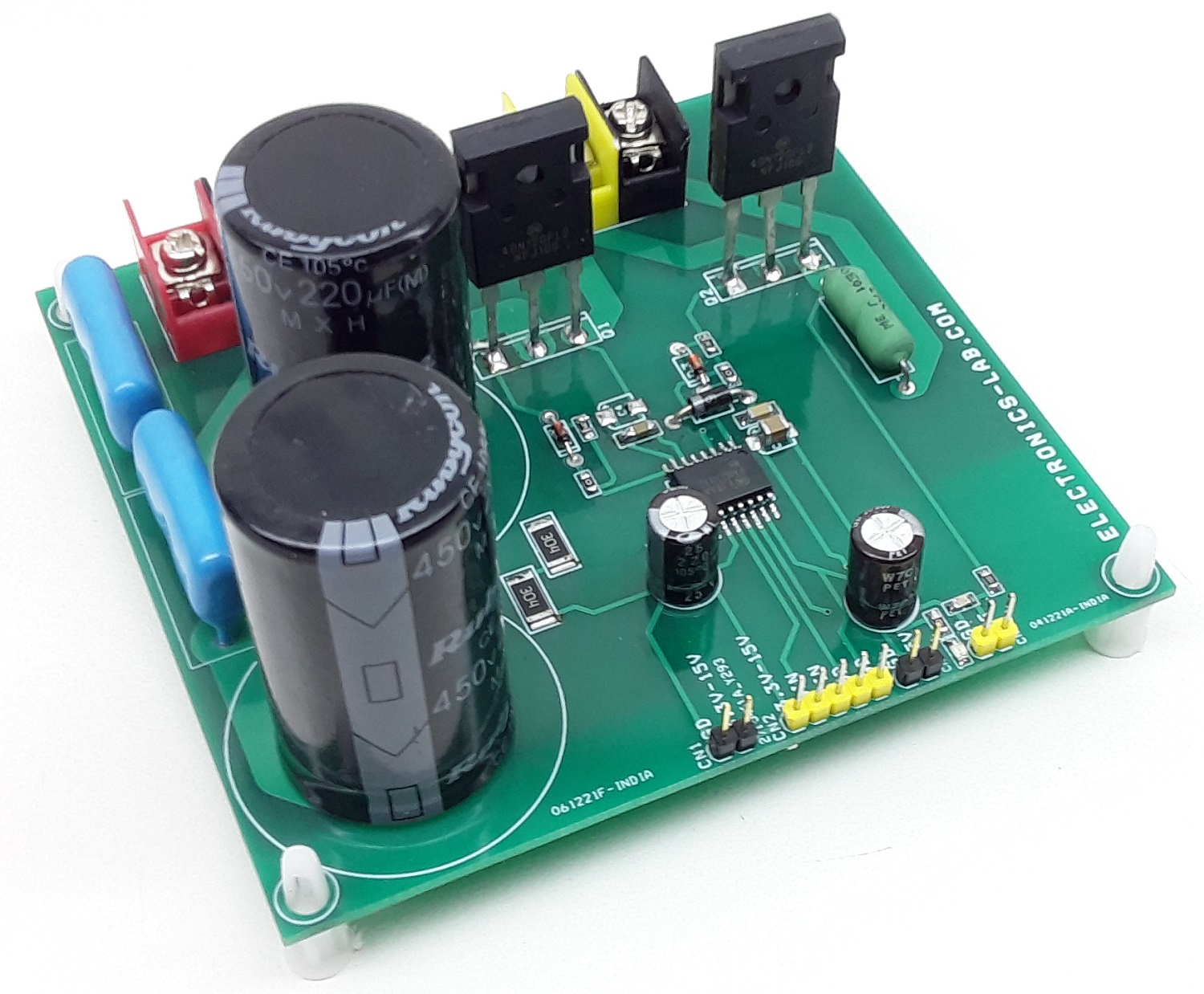
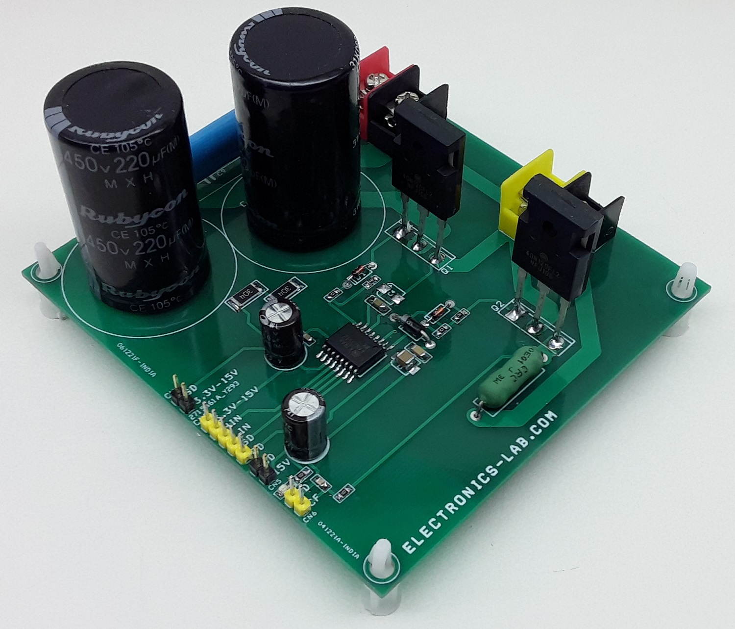
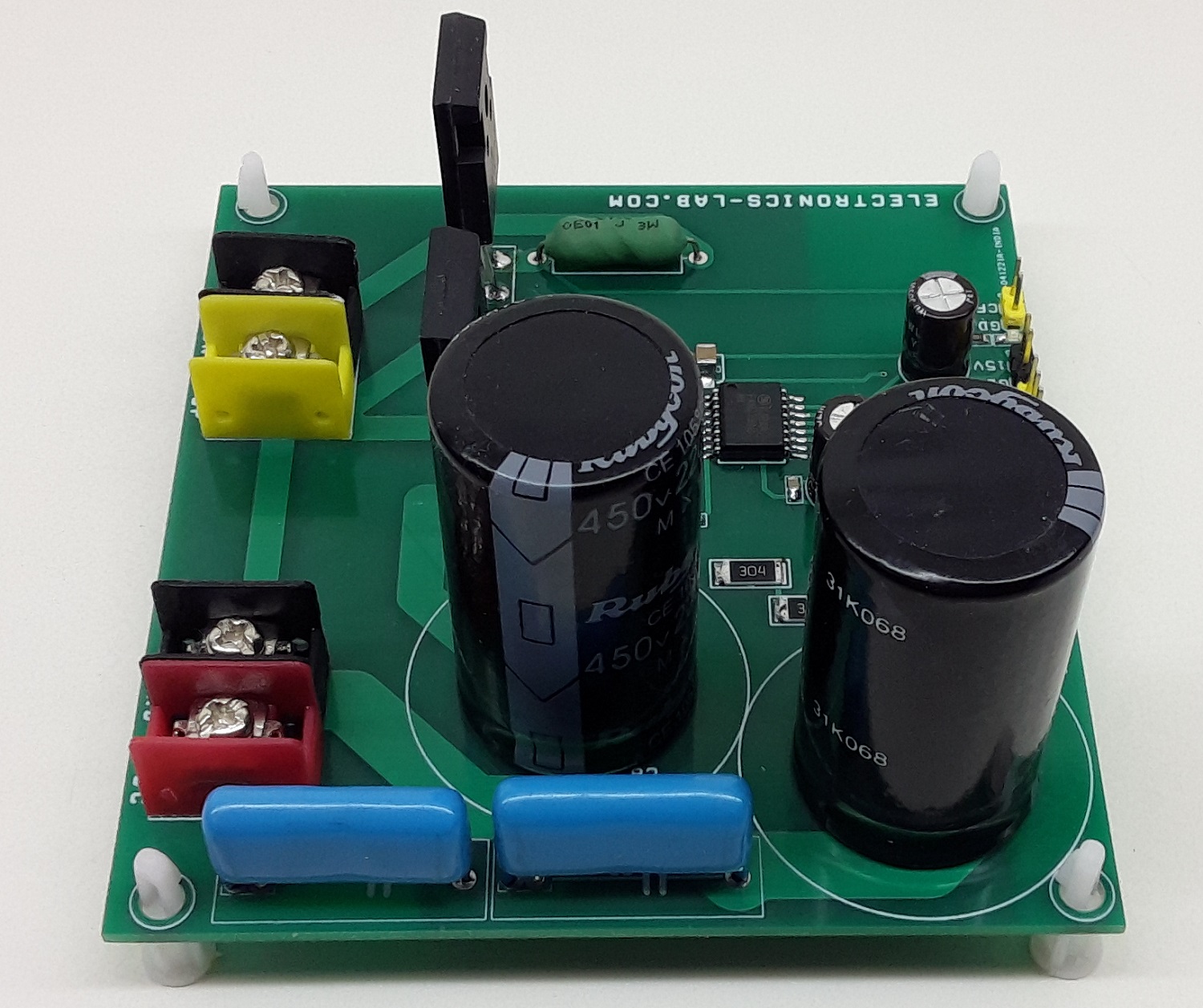
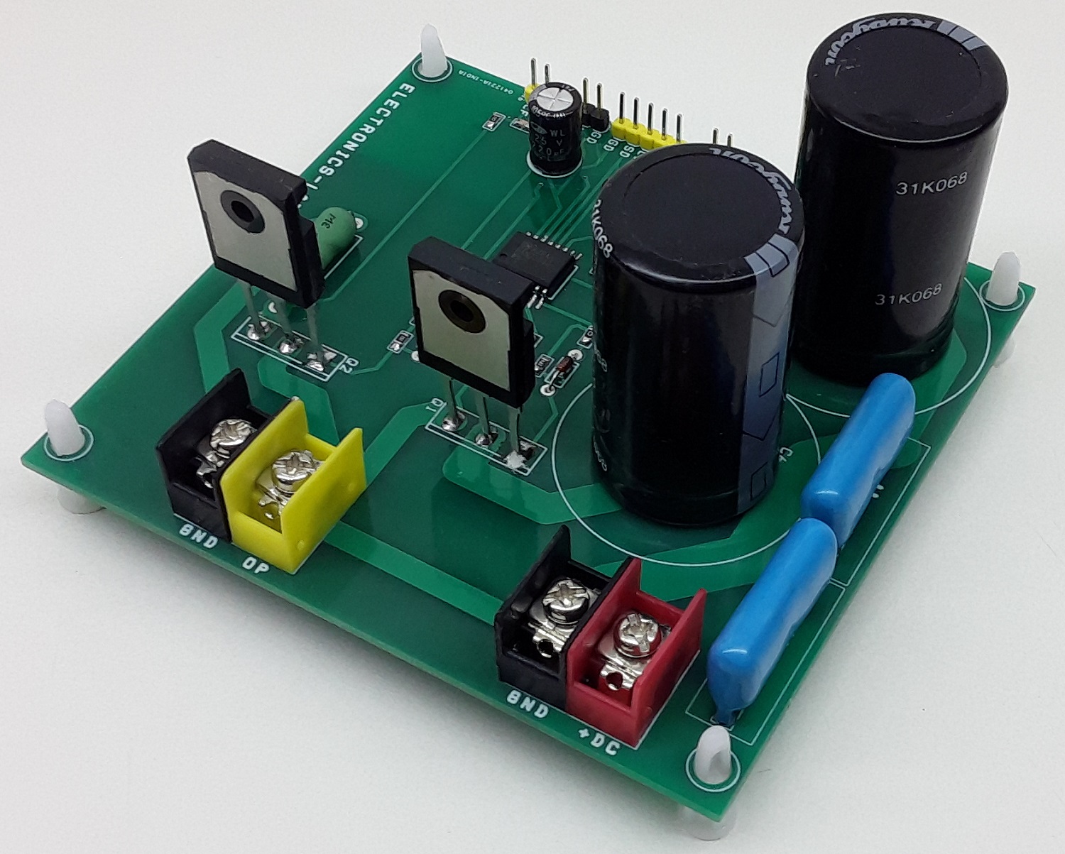
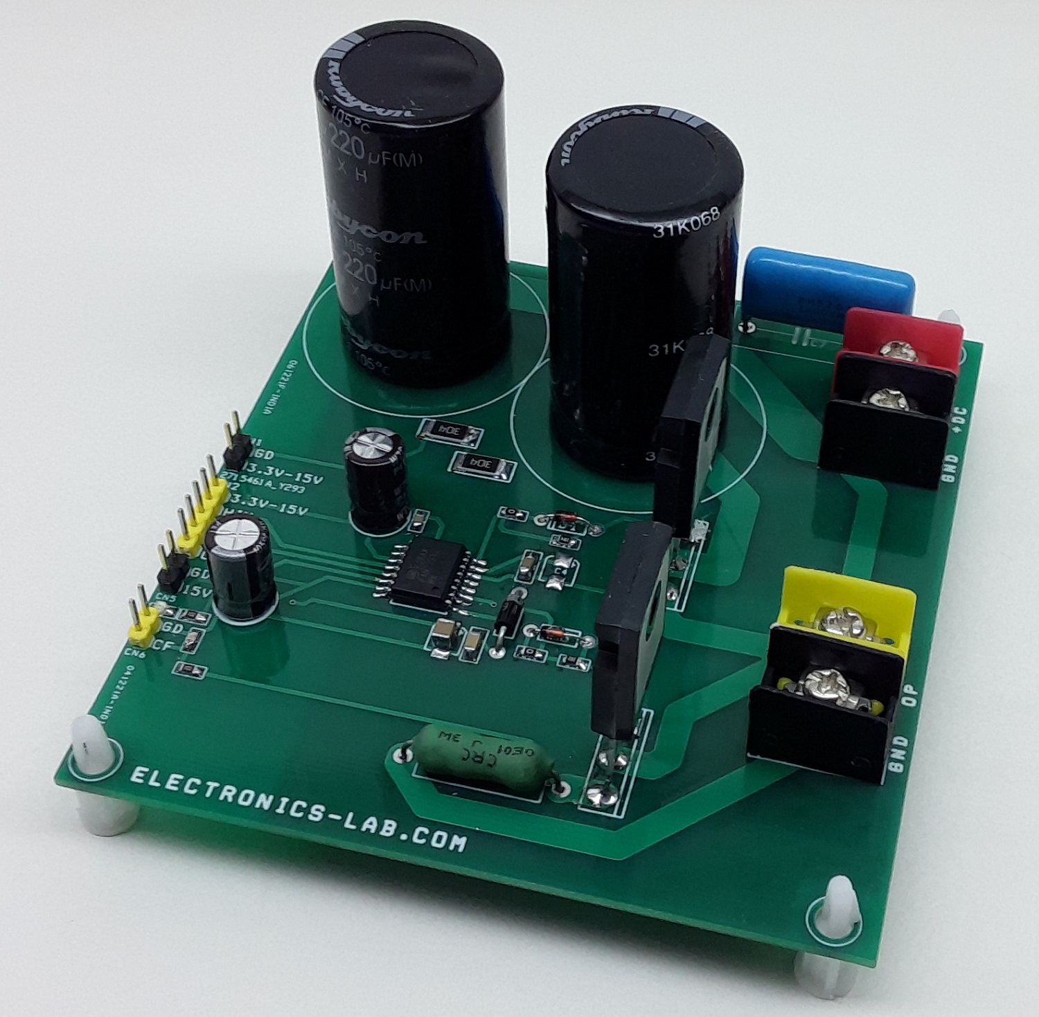
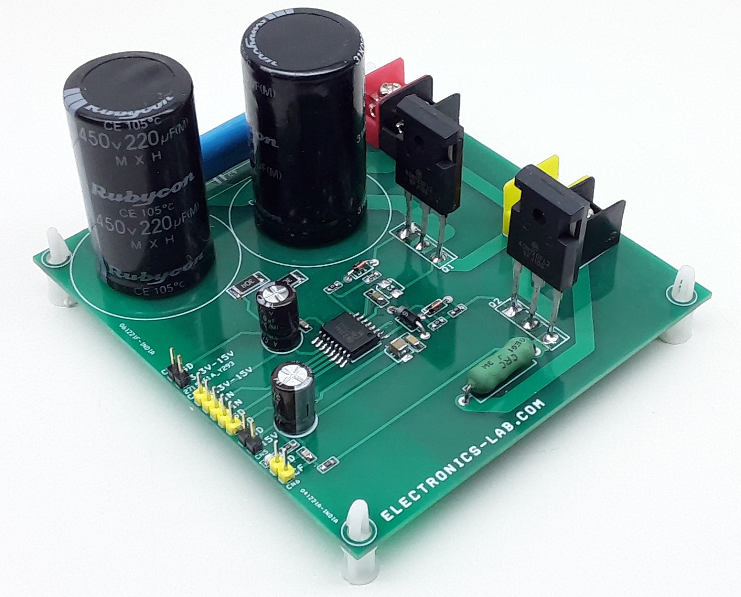
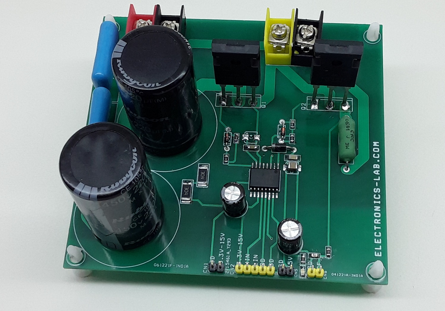
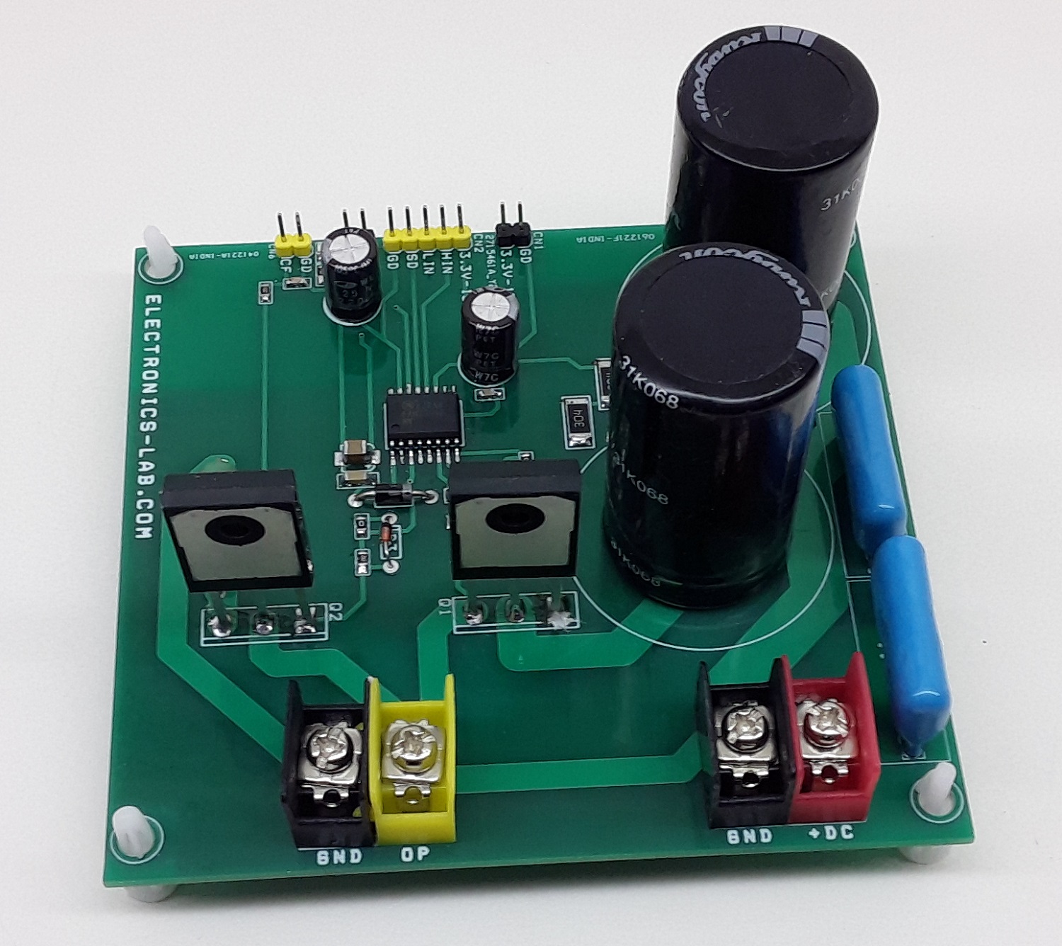
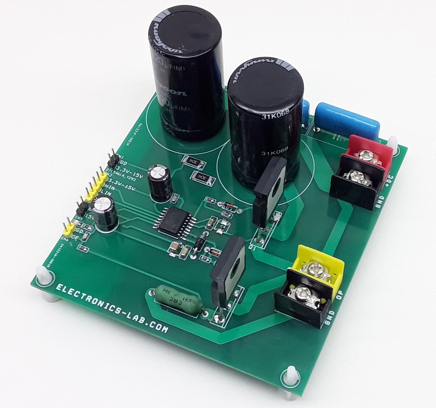
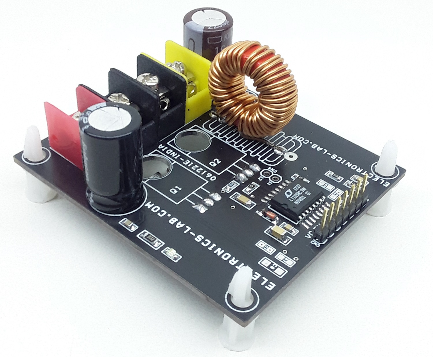
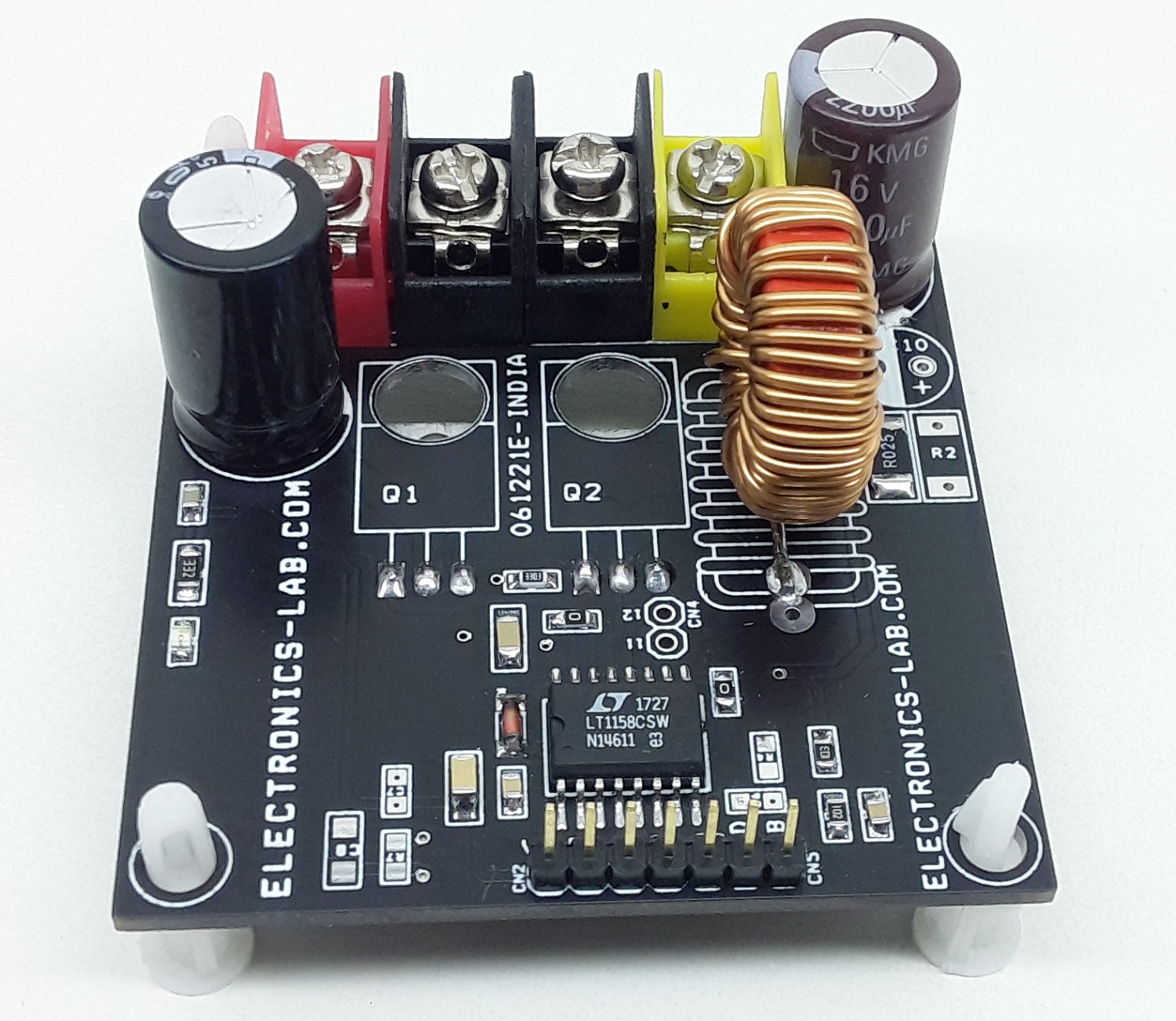
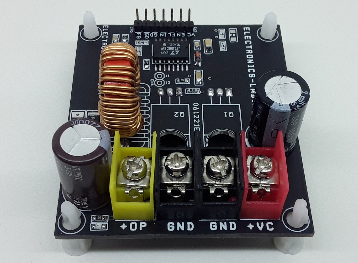
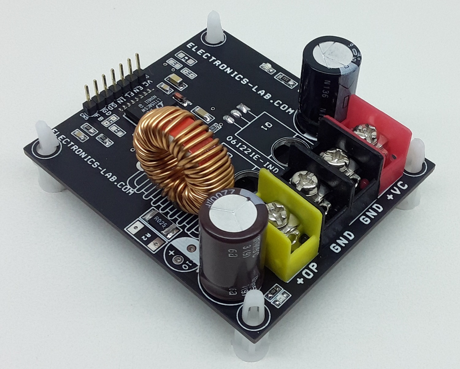
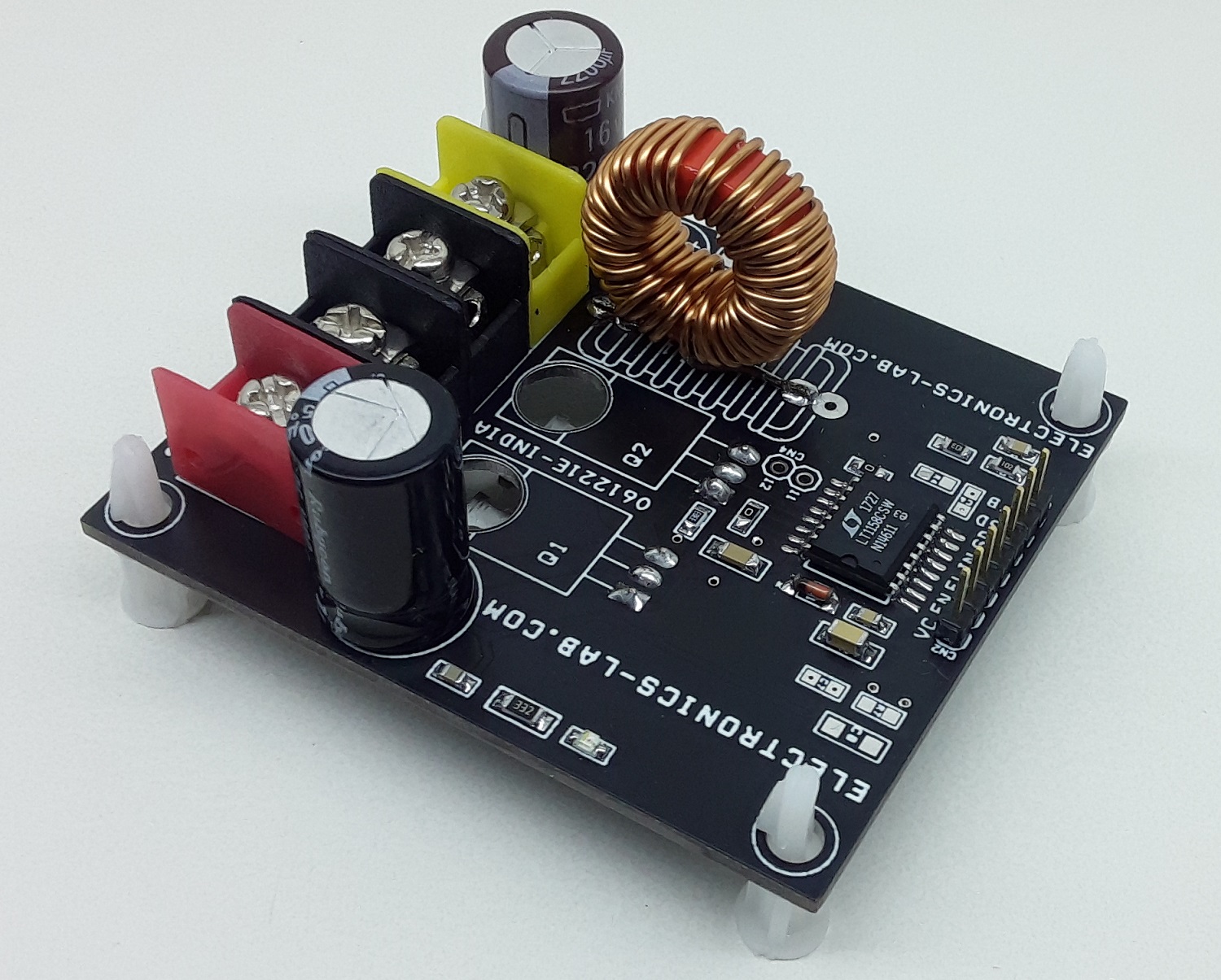
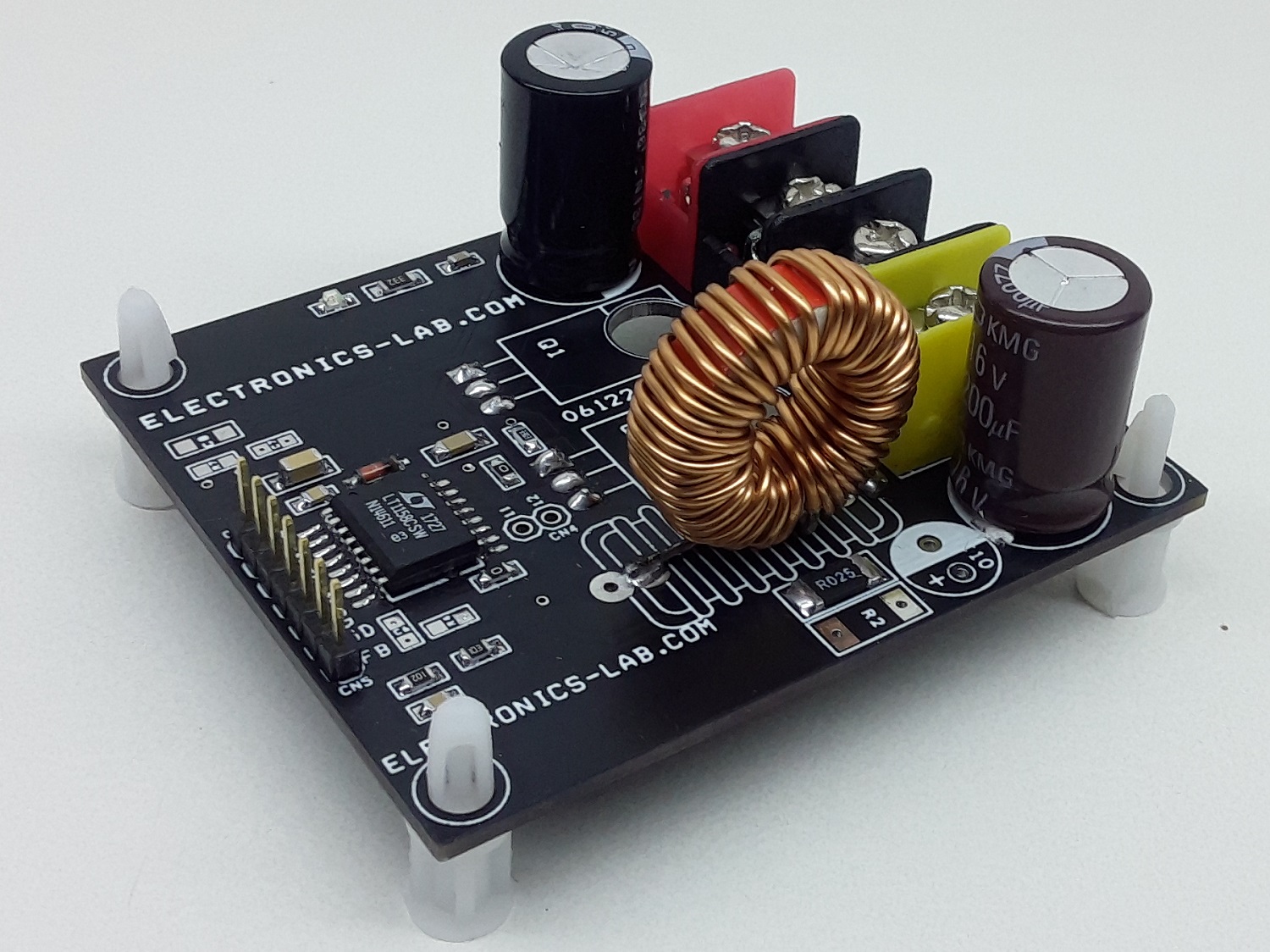
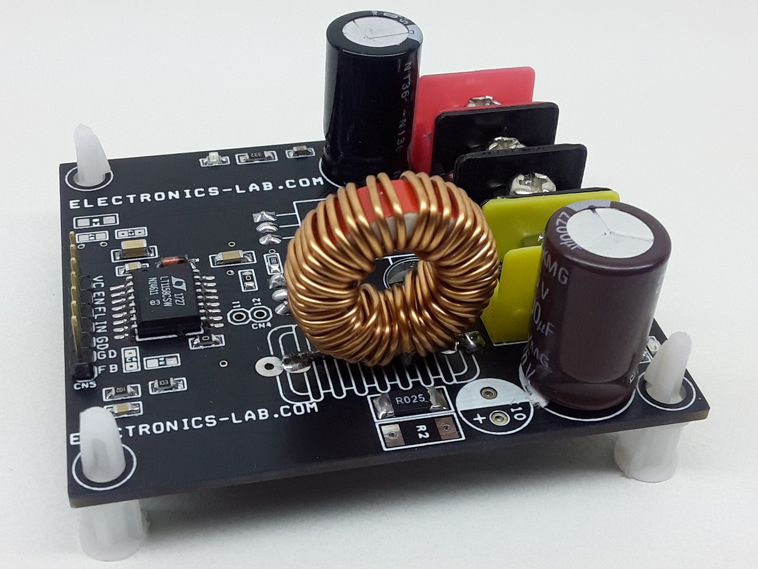
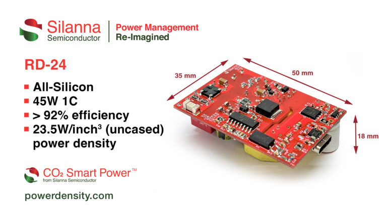
Silanna Semiconductor has further expanded its family of silicon- and GaN-based fast charger reference designs with an all-silicon option that will significantly reduce the time needed to develop high-density 45W applications. Supplied as a fully production-ready solution, the new RD-24 design provides everything needed to rapidly prototype and test a fully functional 45W 1C charger.

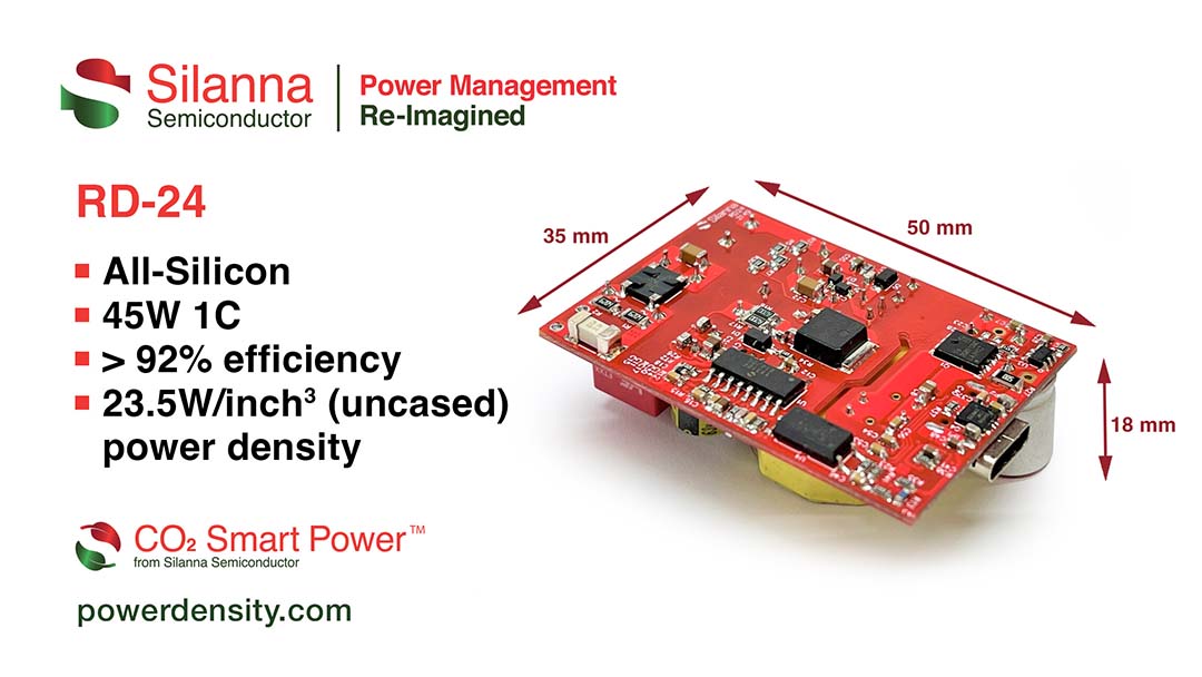
The RD-24 delivers fast charging performance while minimizing overall energy consumption by combining the industry’s best operating efficiency with the lowest ‘vampire’ power consumption. Providing an (uncased) power density of 23.5W/inch3 from a cost-effective single PCB design, the RD-24 operates with a peak efficiency of above 92% and no-load power consumption of below 20mW. Efficiency is flat across the universal input voltage range (90 – 265Vac).

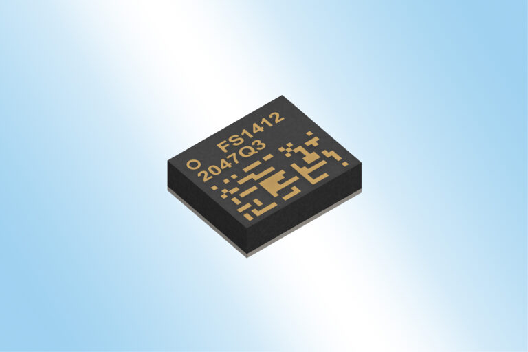
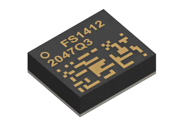
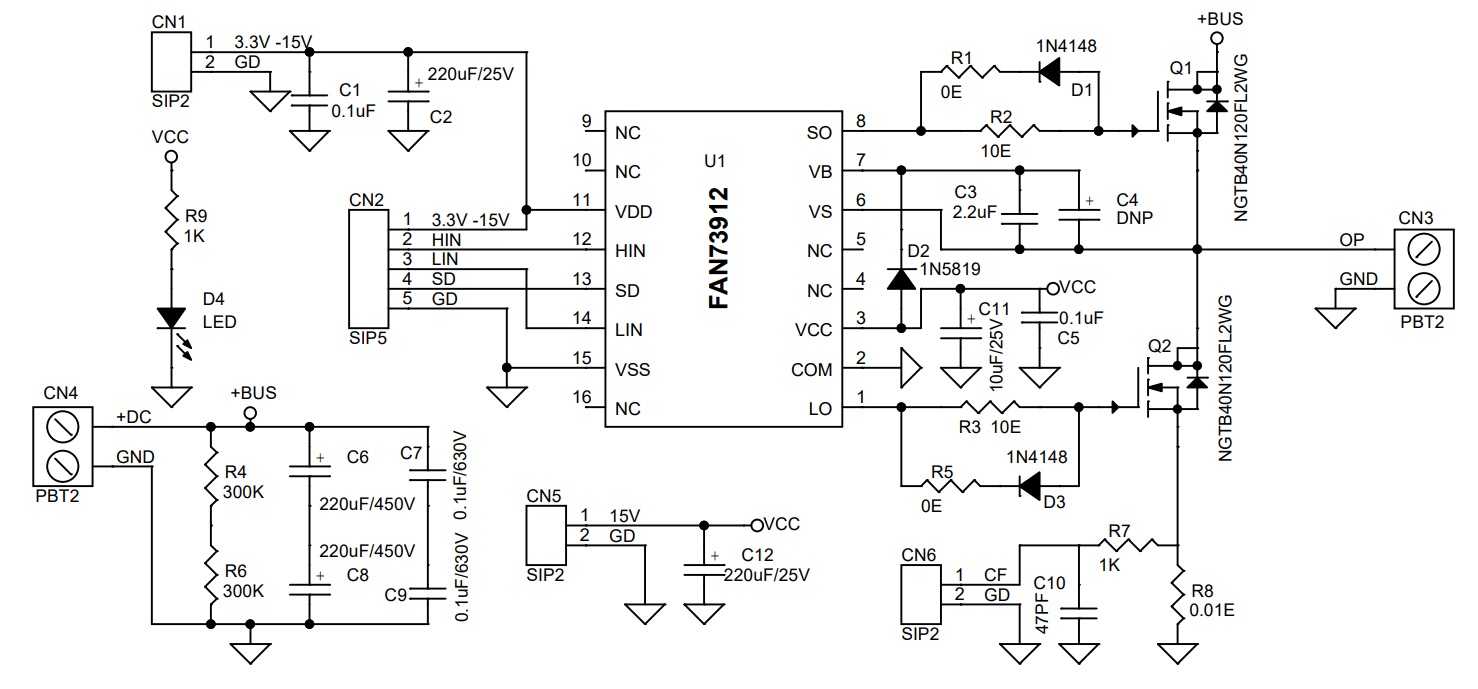
At the heart of the latest reference design is Silanna’s ultra-high-efficiency CO2 Smart Power SZ1131 active clamp flyback (ACF) controller, which is rated for powers up to 65W in universal input designs and above 100W in PFC supported applications. This controller offers a much higher level of integration than has previously been available by incorporating an adaptive digital PWM controller, ultra-high-voltage (UHV) active clamp FET, active clamp gate driver, and startup regulator into a single compact device.

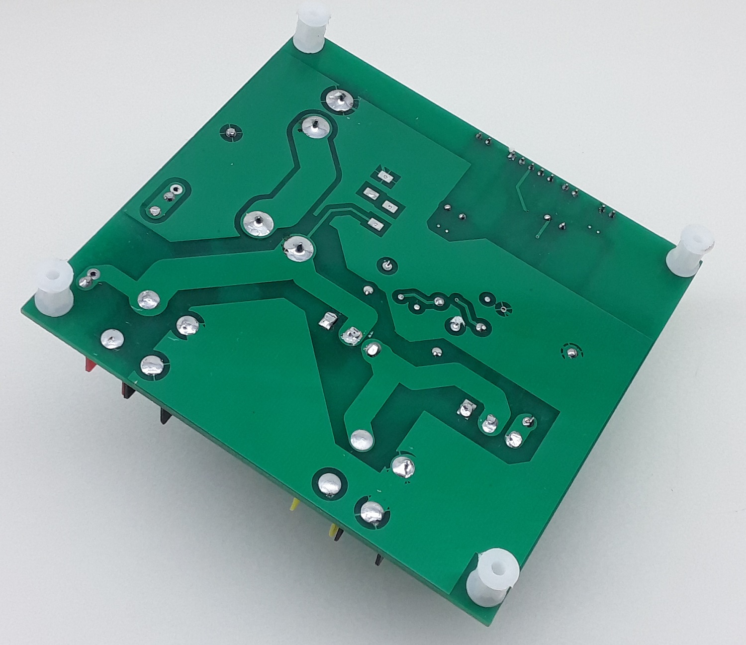
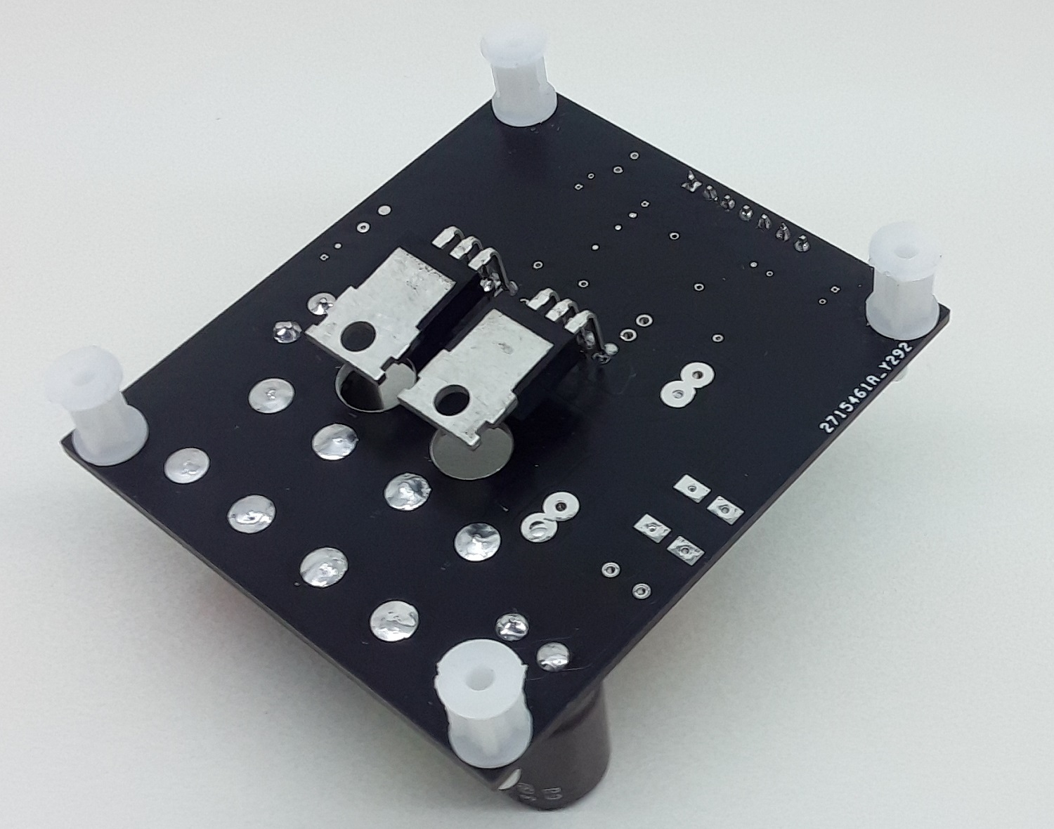
The RD-24 joins a comprehensive family of production-ready reference designs that provide everything needed to develop high-density chargers with low operational and no-load/ standby power consumption and minimum component count, BOM cost, and size. This family includes all-silicon 33W and silicon- and GaN-based 65W USB-PD reference designs. All of these designs exceed conducted and radiated EMI requirements from 3dB to 6dB to eliminate the need for pre-production validation and certification. RD-24 utilizes a single-PCB-based design for the ease of production and assembly, which further reduces the cost for the end customer. Full availability of PCB Gerber and production files reduces the time from prototyping to full production.

RD-24 Key Features

  • 45W 1C high-power-density (23.5W/inch3 uncased) reference design
  • More than 92% peak efficiency
  • Less than 20mW system-level no-load power consumption
  • More than 6dB conducted and less than 3dB radiated EMI margins
  • Flat efficiency across universal (90 – 265Vac) input voltage and load
  • Uses Silanna Semiconductor’s newest fully integrated ACF controller (SZ1131)
    • SZ1131 integrates ACF controller with UHV active clamp FET, active clamp driver, and start-up regulator
    • Up to 146kHz switching frequency operation
    • Ultra-low no-load power consumption
    • OptiMode™ cycle-by-cycle adaptive digital control
    • Self-tuning valley mode switching (VMS)
    • Multi-mode operation (burst mode, QR, VMS)
    • OTP, OVP, OCP, OPP, and Output Short Circuit Protections
  • CO2 Smart Power by Silanna Semiconductor

The SZ1131 operates at frequencies up to 146kHz and provides the ease-of-design of a simple flyback controller with all the benefits of an ACF design. This includes recycling the leakage inductance energy of the flyback transformer and limiting the primary FET drain voltage spike during turn-off events. Employing Silanna Semiconductor’s OptiModeTM digital control architecture, the SZ1131 adjusts the device’s mode of operation on a cycle-by-cycle basis to maintain high efficiency, low EMI, fast dynamic load regulation, and other key power supply parameters in response to varying line voltage and load conditions.

Supplied in a 16-pin SOIC package, the SZ1131 offers protection against over-temperature, over-voltage, over-current, over-power, output short circuit, and transformer core saturation faults without the need for additional external components.

RD-24 Key Features include: 45W 1C high-power-density (23.5W/inch3 uncased) reference design; More than 92% peak efficiency; Less than 20mW system-level no-load power consumption; More than 6dB conducted and less than 3dB radiated EMI margins; Flat efficiency across universal (90 – 265Vac) input voltage and load; Uses Silanna Semiconductor’s newest fully integrated ACF controller (SZ1131); SZ1131 integrates ACF controller with UHV active clamp FET, active clamp driver, and start-up regulator; Up to 146kHz switching frequency operation; Ultra-low no-load power consumption; OptiMode cycle-by-cycle adaptive digital control; Self-tuning valley mode switching (VMS); Multi-mode operation (burst mode, QR, VMS); OTP, OVP, OCP, OPP, and Output Short Circuit Protections; CO2 Smart Power by Silanna Semiconductor;

Conduction-cooled ac-dc supplies deliver up to 1.2 kW, 93.5% efficiency in a compact form factor

Advanced Energy introduced the Artesyn LCC1200 series of fanless, conduction-cooled AC-DC power supplies. The latest addition to AE’s LCC family, the LCC1200 delivers up to 1,200 W power output and 93.5% efficiency in a compact form factor. The new power supplies are well-suited for industrial applications including outdoor digital LED signage, traffic light equipment, industrial lighting, telecommunications antenna, and commercial off-the-shelf (COTS) solutions.

Unlike other power supplies in the market that require output derating above 55°C, the LCC1200 can maintain its full 1,200 W load capacity from -40 to 85°C baseplate temperature without forced air. With 15 W/in3 power density, one of the industry’s highest, the LCC1200 enables customers to save space and reduce overall system cost. Active current sharing is supported and up to three units can be operated in parallel to support higher load requirements.

Measuring only 4.5 x 11 x 1.57 inches, the LCC1200 series is available in IP20 and IP65 ratings. The IP65 version is housed in a robust, fully-sealed enclosure to protect against dust and water ingress, making it well-suited for fanless outdoor and enclosed industrial applications.

With a universal 90-264 Vac input, the LCC1200 series can be used anywhere in the world without adjustment. The power supplies feature a single 28 or 24 VDC output with wide adjustment and 5 V standby voltage output. The LCC1200 family is fully approved to the international IEC62368-1 ITE safety standard and carries cUL, CE, UKCA, and CCC certifications. The built-in PMBus interface provides flexible and comprehensive digital communication with control and monitoring functions for voltage, current, temperature, and reporting of fault conditions. The LCC1200 has a calculated MTBF of more than two million hours and comes with a three-year warranty.

Dual-channel low-side 4/5-A gate driver ICs handle fast MOSFET, WBG switches

Infineon Technologies AG has released the new EiceDRIVER 2EDN product family. Aiming at space-limited designs, the next-generation devices complement the existing 2EDN driver ICs by providing higher system-level efficiencies, excellent power density, and consistent system robustness with fewer external components. Building upon this expansion, the 2EDN family is now able to drive the power switch device performance in applications such as servers, telecomDC-DC converters, industrial SMPSEV charging stationsmotor control, low-speed light electric vehiclespower toolsLED lighting, and solar energy systems.

 The new EiceDRIVER 2EDN family comprises robust dual-channel low-side 4 A/5 A gate driver ICs. It is targeting not only fast power MOSFETs but also wide bandgap (WBG) switching devices. The gate drivers enable engineers to meet their design requirements in many different package sizes, ensure safe turn-off before under-voltage lock-out (UVLO) and achieve faster UVLO reaction for robust operation and noise immunity.

The fourteen new devices come in a broad range of packages. Besides the well-known 8-pin DSO, TSSOP, and WSON package options that allow compatibility and drop-in replacement, Infineon now offers the world’s smallest 6-pin SOT23 package (2.8 x 2.9 mm 2) and TSNP package (1.1 x 1.5 mm 2) variants. SOT23 and TSNP packages eliminate the enable (EN) signal, which frequently is not used. As a result, they are able to offer the perfect balance for space-limited designs leading to higher power density and higher Temperature Cycling on Board (TCoB) robustness.

Designers can choose between 4 V and 8 V UVLO options for instant power switch protection under abnormal conditions. Essentially, the new products bring better UVLO filtering time, a faster wake-up from UVLO off status and more than two times faster UVLO reaction from start-up and burst mode. Moreover, they feature high precision, accurate rail-to-rail outputs, and fast active output clamping at V DD = 1.2 V, typically clamping in just 20 ns for extra robustness.

[via www.eeworldonline.com]

Ultra-low profile dc-dc converters power 12-A loads

TDK Corporation announces the availability of the FS1412 microPOL (μPOL) power module. At 5.8. mm, x 4.9 mm x 1.6 mm, the FS1412 is part of a new series of µPOL DC-DC converters with increased performance, smallest available size, ease of use, and simplified integration for applications such as big data, machine learning, artificial intelligence (AI), 5G cells, IoT networking, telecommunication, and computing enterprise. μPOL technology includes a DC-DC converter placed in the vicinity of complex chipsets such as ASICs, FPGAs, and others. By minimizing the distance between the converter and the chipset, the resistance and the inductance components are minimized, allowing fast response and accurate regulation with dynamic load currents. Mass production of FS1412 started in Q4 2021.

TDK has been developing this technology over several years to enable system-level solutions to enhance electrical and thermal performance focusing on high-density cost-effective solutions for space-constrained applications which require a low-profile power source. These new solutions incorporate high-performance semiconductors in advanced packaging technologies such as semiconductors embedded in a substrate (SESUB) and advanced electronic components to achieve unique system integration in a smaller size and lower profile by 3D integration. This integration allows TDK to deliver higher efficiency and ease of use at a lower total system cost than what is currently available.

The new µPOL DC-DC converters series operates at a broad junction temperature range, from -40 °C to 125 °C, and features a high current density of more than 1000 A per cubic inch. The series delivers at 12 A with the lowest commercially available height at 1.6 mm while offering 50% less solution size than the other products available in its class. As a result, this minimizes system solution cost, reduces board size and assembly costs, as well as BOM and PCB costs.

more information: https://product.tdk.com/en/search/power/switching-power/micro-pol/info?part_no=FS1412-0600-AL

Binder Jetting vs CNC Machining: Which is Better for Rapid Prototype?

Have you ever requested a third-party rapid prototyping services provider to fabricate samples for testing? If so, you were likely offered either 3D printing or CNC machining as options.

Sometimes customers have a difficult time trying to decide that prototyping method suits their manufacturing purposes better. This post provides an in-depth comparison of 3D printing, to be exact, binder jetting, and CNC machining. So that you can know for sure that will work better for you.

Types of Rapid Prototyping

Well, there are numerous types of rapid prototyping, all of which can be attributed to either subtractive manufacturing (SM) or additive manufacturing (AM) techniques. The first one implies that the material is cut out of a workpiece to achieve the design required.

The following manufacturing techniques are attributed to SM rapid prototyping:

  • CNC machining
  • Metal casting prototyping
  • Metal extrusion prototyping
  • Sheet metal prototyping

The second rapid prototyping technique is grounded on adding material layer by layer to achieve the design required or a similar principle. All such types are known as different 3D printing techniques. The following manufacturing types of 3D printing are attributed to AM rapid prototyping:

  • Binder Jetting
  • Selective Laser Sintering (SLS)
  • Fused Deposition Modeling (FDM)
  • Stereolithography (SLA)
  • Multi Jet Fusion (MJF)
  • Injection Molding
  • Injection molding

As you may see, the number of rapid prototyping options available is extensive. To help you not to get lost in what to choose, we detail the essential aspects of metal machining and the popular 3D printing technique – binder jetting below.

Binder Jetting

Definition

Binder Jetting is an AM technique that is based on creating a 3-dimensional object layer by layer in accordance with a computer-aided design (CAD) file.

The principle of binder jetting is the use of the metal powder material that is solidified with a binding agent layer by layer. First, a piston of a binder jetting machine ensures that the powder is compressed dense enough for binding. Then, powder in the build box is cured with a binding liquid forming a solid shape. Then, with the use of brushes and air blowers, the excess powder is removed.

After the binder jetting is finished, simple post-production procedures are needed. The printed parts are separated from build boxes, cleaned, and bead blasted. You may also perform additional finishing techniques to enhance the properties of parts printed using binder jetting.

Pros and Cons

Here’s the list of the main strengths of binder jetting as a particular method of 3D printing:

  • One of the quickest rapid prototyping processes overall
  • Complete design freedom
  • Minimal material wastage
  • Simple, single-step manufacture
  • Cost-effective process
  • High accessibility of binder jetting machines, spare parts, and printing materials
  • Environment-friendly
  • Safe for labor

And the notable weaknesses of the process:

  • Limited range of materials available
  • Limited dimensions of components that are possible to print
  • Require post-processing, but some techniques still do not enable good surface finishing
  • The structure of printed components typically makes prototypes unsuitable for physical properties testing

Application

This AM technique is widespread in the following industries:

  • Architecture and construction
  • Maritime industry
  • Healthcare
  • Chemical industry
  • Mechanics
  • Food processing industry
  • Aeronautics
  • High-tech
  • Retail
  • Automotive
  • Textile and fashion
  • Robotics
  • Optics
  • Electronics
  • And many others

3D printing enthusiasts use binder jetting to replace literally any goods that can only be printed. The capabilities of binder jetting are limited only with the phantasy of such equipment unit’s owners. Still, binder jetting has even wider industrial use for the production of goods.

Precision sensor probe inspection of gear. Quality control in metalwork. Metrology system for gear

CNC Machining

Definition

CNC machining is an SM technique based on creating a 3-dimensional object by cutting out pieces of material of a workpiece according to a G-coded CAD file. The range of machining operations that can be done using multiple CNC machines is vast and include the following:

  • Drilling
  • Milling
  • Boring
  • Facing
  • Planing
  • Sawing
  • Broaching
  • Reaming
  • Turning
  • And others

Machines that perform CNC machining are automated, computer-driven centers with spindles that hold cutting tools and move along multiple (4,5,6, and even more) dimensions. They cut metal chips off workpieces’ surfaces, ensuring high dimension accuracy.

CNC machines are named after the process they intended to perform (although advanced centers employ multiple operations). This list includes mills, routers, drills, lathes, turning machines, etc.

Pros and Cons

Here’s the list of the main strengths of CNC machining:

  • Continuous use of machines without labor involvement
  • Consistency from batch to batch
  • Great dimensional accuracy and precision
  • High quality of the surface
  • Components machined are fully suitable for properties testing
  • Cost-effective process, but only if a significant number of products is machined
  • Good design freedom
  • A vast range of materials is supported

And the notable weaknesses of the process:

  • Time-consuming process
  • Demanding to the expertise of the labor
  • Not always ensure single-step manufacture
  • Machines are difficult in maintenance and adjustment
  • Material wastage
  • May not be environment-friendly
  • Is dangerous for labor unless safety measures are taken

Application

Decades ago, manual machining was a prevalent method of fabrication. It is not surprising that in the following contemporary industries, CNC machining is the common manufacturing technique for rapid prototyping as well:

  • Architecture and construction
  • Healthcare and pharmacy
  • Food processing industry
  • High-tech
  • Automotive
  • Robotics
  • Optics
  • Electronics
  • Military and defense
  • Aerospace
  • Transportation
  • Oil and Gas
  • And nearly any other somewhat

CNC machining utilizes fully automated centers that employ subtractive machining to fabricate components. Rapid prototyping with the use of CNC equipment units is highly common and regarded as a great way to produce samples for testing.

Differences Between Binder Jetting and CNC Machining

Regarding the essential differences between these two manufacturing processes, all existing ones are detailed in the table below.

Factor Binder Jetting CNC Machining
Principle of functioning Additive machining Subtractive machining
Type of files required CAD files G-coded CAD files
Parts’ dimensions supported Strictly limited. Depends on the type of binder jetting machine. Almost unlimited. Depends on the method of metal machining and the type of CNC unit used.
Material availability A limited range. Each method has its own small range of materials supported. A vast range. Almost unlimited, depending on the method of metal machining and the CNC unit used.
Speed of prototyping A single unit ensures end-to-end performance. Speed depends on the design.

A single prototype can be produced quickly.

Several units may be involved in the end-to-end performance. Speed depends on the design and the number of CNC units.

A single prototype can be produced slowly.

Accuracy / Precision Good dimension accuracy. Superior dimensional accuracy.
Repeatability / Consistency Consistency may vary from batch to batch. Ensures a high batch-to-batch consistency.
Surface quality Appropriate surface quality. In some cases, additional finishing processes may not be applicable. Surface quality depends on the method of metal machining and the type of CNC unit used. Generally, surface quality is high. Suitable for the additional finishing process.
Adherence to physical properties of the intended component. Generally unusable to produce components for further physical and chemical properties of components testing. Exception – when large-scale manufacturing is 3D printing (binder jetting)-based. Depending on the manufacturing method employed, it is generally usable to produce components for further physical and chemical properties of components testing.
Complexity of use Comparatively simple process. Does not require specialized knowledge. Comparatively complicated process. Require a highly professional team of specialists to run.
Flexibility Highly flexible process. Nearly any design can be created using a single equipment unit. Less flexible process. Most designs can be created, depending on the method. May require the use of multiple equipment units.
Cost Low to medium price range, depending on the process and the material. Medium, to high price range, depending on the process and the material.
Material wastage Produce nearly no material wastage. Is typically associated with high material wastage.

In this comparison, a winner cannot be determined. Depending on your exact needs, materials, requirements to a prototype, timelines, and other factors, you may find any of the techniques being completely applicable.

Final Word

CNC machining is a costly and not that quick technique for fabricating durable prototypes of workpieces. It is great for testing manufacturing techniques and the physical properties of samples.

In contrast, binder jetting is indeed a rapid and cost-effective additive manufacturing prototyping technique. It is great for taking a quick look at newly modeled designs or producing cheap samples for presenting stakeholders. You should guide your decisions based on careful consideration of the factors specified in this post.

[photos: depositphotos.com]

The Benefits of Multilayer PCBs

PCBs or Printed Circuit Boards are the fundamentals of every modern electronic device. They are used in various devices such as computers, smartphones, GPS devices, and many others.

There are various types of PCBs that include single-sided PCBs, double-sided PCBs, flexible PCBs, rigid PCBs, and many others. However, some PCBs are simple, while others are a bit complex.

To learn more about Multilayer PCBs, here is a simple guide about Multilayer PCBs, their uses, and benefits in the world of electronics.

What is Multilayer PCB?

Multilayer PCB is a printed circuit board with three or more copper foil layers. These are several layers of double-sided PCBs that are glued and laminated together with heat-protective insulation.

Multilayer PCBs were designed due to various changes in the electronic world. And in today’s world, the tasks of electronic devices have become more refined. Hence, they require complex PCBs such as multilayer PCBs.

However, most traditional circuit boards had many issues, such as noise and being very heavy. In addition, they needed to follow specific design constraints.

Due to these issues, it was hard to get a good level of performance. Thus, multilayer PCB was invented. Multilayer PCBs are small, lightweight, and durable.

In addition, multilayer PCBs are used in various sectors such as automobile, defense, medical, and many others. They are used in almost every complex electronic gadget.

They are available in many sizes and widths to handle the needs of any electronic gadgets. Layers are generally in even numbers since odd numbers can bring circuit problems such as warping.

Most applications need between four to eight layers, even though devices such as smartphones use around twelve layers. But some PCB manufacturers produce multilayer PCBs with almost a hundred layers.

Although multilayer PCBs are a bit more expensive than simple PCBs, they have become very popular due to the numerous benefits.

Small electronics integrated circuit IC on empty printed circuit board ready for hand assembly

Benefits of Multilayer PCBs

Multilayer PCBs are used in various electrical gadgets because they offer numerous advantages in functions, design, and cost. Here are the main benefits of multilayer PCBs.

1. Small Size and lightweight

The main benefits of multilayer PCBs are their lightweight and size. Due to their smaller size than other PCBs, they are beneficial to most modern electronics.

Hence, it is now possible to have a smaller device but very powerful. Some of these gadgets include laptops, tablets, and smartphones.

With a smaller PCB, it means less weight. Hence, most multilayer PCBs are smaller and very light. This is a benefit to most modern electronic devices moving towards mobility.

2. High quality and durability

Multilayer PCBs are of high quality and very durable from designs to planning. They are of better quality than single-sided PCBs and double-sided PCBs. In addition, they are more reliable.

Also, multilayer PCBs are more durable than other PCBs. They are designed to handle heat and pressure and their own weight.

3. Improved flexibility

Even though not all multilayer PCBs are flexible, you can find a flexible multilayer PCB. The flexible one is essential for some applications where mild bending is needed.

4. More Powerful

Multilayer PCBs are robust and other PCB types. Hence, they can achieve greater capacity and speed even if they are smaller in size.

With the above benefits, multilayer PCBs are useful in a wide range of applications, especially mobile gadgets. And with most industries going mobile, multilayer PCBs are mostly preferred over other PCBs.

Benefits of multilayer PCBs over Single-layer PCBs

Compared to single-layer PCBs, multilayer PCBs come with numerous advantages. Some of the advantages include:

  1. Higher assembly density – since single-layer PCBs are limited by their surface area, multilayer PCBs increase their density through layering.

The increased density increases functionality, enhanced capacity even though they are smaller and lightweight.

  1. Smaller size – generally, multilayer PCBs are smaller than single-layer PCBs. Instead of increasing the size of the surface area, multilayer PCBs have extra layers.
  2. Improved design functionality – multilayer PCBs are more than an average single-layer PCB. Hence, they can accomplish more despite their smaller size and lesser weight.

What are Multilayer PCB Applications?

Multilayer PCBs have become the preferred option for various applications. Some of the leading multiplayer PCB applications include:

  • Consumer electronics – consumer electronics are the primary devices that use multilayer PCBs. Since most consumer electronics such as smartphones, laptops, and smart-watches are multi-function, they need refined PCBs.
  • Computer electronics – Most electronics use multilayer PCBs due to their small size and high functionality. In addition, they are perfect for many technologies in the computer industry.
  • Telecommunications – telecommunication gadgets such as GPS, signal transmission, and satellite use multilayer PCBs. The main reason is because of their functionality and durability.
  • Medical devices – multilayer PCBs are also used in many medical devices due to their small size, impressive functionality, and are lighter than single-layer PCBs.
  • They are used in CAT scan equipment, X-ray equipment, heart monitors, and medical testing devices.
  • Military – since multilayer PCBs are durable, light, and have impressive functionality, they are favored in the military sector.
  • Automotive – most cars rely on electric components in this modern era. The auto industry uses multilayer PCBs on GPS devices, computers, headlight switches, and many others.
  • Since they are durable and small, multilayer PCBs are functional and fit for any automobile.
  • Aerospace – just like cars, planes and jets have computers and other electronics that use PCBs. Hence, multilayer PCB offers an ideal solution for aerospace.
  • Others – multilayer PCBs are used in other industries such as the research industry, science, security, and some home appliances.  

Final Word

Multilayer PCBs come with numerous benefits over single-layer PCBs. Hence, they are preferred for various applications. They are durable, lightweight, small, and very effective.

Due to their benefits, the number of multilayer PCB uses continues to expand. More and more industries are focusing and investing in multilayer solutions. Hence, it would help if you focused and partnered with PCB manufacturers.

[photos: depositphotos.com]

Top 10 of 3D Printing Services with Instant Online Quote

Whether you are new to 3D printing technology or just looking to close a few knowledge gaps, I am glad you stopped by. By now, most of us have heard of the potential of 3D printing at some level, but I do believe most of us did not know much about the 3D printing services and get lost in multiple choices on the Internet. As a hardware engineer, I would like to recommend the top 10 3D Printing Services, hope it can meet your needs.

1. JLCPCB 3D Printing jlcpcb.com/3d-printing

JLCPCB is a worldwide leading PCB supplier is famous for its cost-effective PCB prototype service, 3D printing service is newly launched in 2022 and its instant online quote system is very well designed, you can get the price after the CAD file upload instantly and also will get an image for your finished product by 3D model viewer below it

.JLCPCB 3D printing service is quite suitable for rapid prototyping – customers will profit from industrial-grade printers and dedicated technical support. And they made the cost for 3D printing prototype as low as $1 and the lead time within 48 hours.

OVERVIEW

  • Instant online quote
  • Materials: Nylon (SLS/MJF), PA 11, PA 12-GB (SLS/MJF), Resin, TPU (SLS), Aluminum, Steel, Plated Metal, Brass, Silver, Gold, Bronze, Sandstone
  • Formats: STL, Collada, OBJ, X3D(B), VRML2
  • Payment: Credit Card, PayPal, Bank Transfer,Jpay

2. Shapeways shapeways.com

As the world’s most popular online 3D printing service, Shapeways offers two services. On the consumer side, you can choose from a broad array of professionally designed items, customize them, and have them printed to your specifications. Similar to other 3D printing services, Shapeways hosts storefronts for designers to sell models, printing the sales for them. Shapeways is also suitable for rapid prototyping – customers will profit from industrial-grade printers (EOS, 3D Systems) and dedicated technical support.

OVERVIEW

  • Shipping Worldwide
  • Instant online quote
  • Materials: Nylon (SLS/MJF), PA 11, PA 12-GB (SLS/MJF), Resin, TPU (SLS), Aluminum, Steel, Plated Metal, Brass, Silver, Gold, Bronze, Sandstone
  • Formats: STL, Collada, OBJ, X3D(B), VRML2
  • Payment: Credit Card, PayPal, Bank Transfer

3. Sculpteo Sculpteo.com

Sculpteo is an online 3D printing service that allows anyone to upload 3D models and have them fabricated in a wide variety of materials. In keeping with its competitors, Sculpteo also allows individuals and professionals to open up an online storefront and sell their designs to the public.

Sculpteo’s stable of professional services positions it as a comprehensive partner for batch production, prototyping, and design validation. A number of online tools, including analysis and repair, plus optimization help you to get the most out of your print.

OVERVIEW

  • Shipping: Worldwide
  • Quotes Instant
  • Materials: Nylon (SLS/MJF), PA12-GB, PA12 Carbon, PEBA, TPU, Alumide, Resin, Stainless Steel, Aluminum, Titanium, Brass, Bronze, Silver, Plated Metal
  • Formats: STL, OBJ, 3DM, 3DS, 3MF, AC3D, ASE, CATPART, CATPRODUCT, CGT, COB, DAE, DXF4, IAM, IPT, IGES, IGS, KMZ, LWO, MD2, MD3, OFF, PLY, PRC, Q3O, RAR, Q3O, RAR, SAT, SCAD, SKP, SLDPRT, SLDASM, STEP, TGZ, U3D, VRML, X_T, ZIP
  • Payment: Paypal, Credit card, bank transfer, check (France only), Sculpteo credit (Sculpteo store-holders only)

4. i.materialise i.materialise.com

i.Materialise is a company that works with industrial clients to produce prototypes and 3D printed products. But for the general public and individual designers, Materialise offers an online 3D printing service called i.Materialise.

Much like Shapeways above, i.Materialise also hosts designer-run shops, allowing creatives to sell their wares as physical items, which are then fulfilled by i.Materialise.

OVERVIEW

  • Shipping: Worldwide
  • QuotesInstant
  • Materials: ABS, TPU, Nylon (SLS/MJF), Alumide, Polypropylene PP, Resin
  • Formats: STL, OBJ, WRL, SKP, Collada (DAE), 3MF, 3DS, IGS, MODEL, 3DM, FBX, PLY, Magics, MGX, X3D, STP, STEP, PRT, MATPART, matAMX, AMF, NDO, ASC, CLI, SLC, MTT, MDCK, CLS, F&S, SSL, SLI, PRJ, SAT, CATproduct, DXF, ZCP, PRT, ASM
  • Payment: Credit Card, PayPal

5. Star Rapid star-rapid.com

Star Rapid offers a wide range of prototyping services for professionals and ambitious hobbyists. The website includes detailed information on the available additive manufacturing technologies and finishing services.

Besides 3D printing, other techniques offered by this 3D printing service include plastic mold injection, CNC machining, pressure die casting, and vacuum casting. So, this company is a candidate in case your needs go beyond rapid prototyping, with low-volume manufacturing also possible. The case studies are a worthwhile read, too, and demonstrate what this company is capable of achieving.

OVERVIEW

  • Shipping: Worldwide
  • Quotes Request Form
  • Materials: Titanium, Steel, Aluminum, Maraging Steel
  • Formats: STL, STEP, IGES
  • Payment: Bank transfer, Paypal

6. Protolabs protolabs.com

Protolabs is a little different in the on-demand manufacturing world because they have figured out how to reduce turn-around times drastically. Their founder used automation to make the entire process perform smoother and faster.

Protolabs offers a metal, elastomer, LSR, and plastic 3D printing service for printing prototypes and parts. They also offer injection molding, CNC machining, and CNC finishing. It is a high-quality 3D printing service with better delivery times than most other services.

OVERVIEW

  • Shipping: Worldwide
  • Quotes Instant
  • Materials: ABS, Nylon (SLS/MJF), Polycarbonate PC (SLA), Polypropylene PP (SLA), Digital Photopolymer, Aluminum, Copper, Stainless Steel, Titanium, Inconel
  • Formats: IGS, STEP, ACIS, X_T, X_B, STL
  • Payment: Invoice, PayPal

7. Kraftwurx kraftwurx.com

Kraftwurx has by far the largest selection of materials, with a whopping amount of 85 materials to choose from. Their site is slightly difficult to navigate through, and you may find it hard to find what you are looking for. Also, Kraftwurx only supports six different 3D file types, so make sure to create or download a 3D file that they support if you choose them.

While Kraftwurx does offer 3D printing, the site is geared more towards e-commerce. You can upload your ideas and use Kraftwurx’s infrastructure to drop-ship your products.

OVERVIEW

  • Shipping: Worldwide
  • Quotes Instant
  • Materials: ABS Plus, Ultem, Polycarbonate PC, Photopolymer PP, Nylon (SLS), Gold, Aluminum, Stainless Steel, Bronze, Ceramic, Copper, Acrylic, Palladium, Casting Wax
  • Formats: STL, OBJ, X3D, DAE, WRL, VRML97/2
  • Payment: PayPal, check

8. Beamler beamler.com

Based in the Netherlands, Beamler is a 3D printing service that relies on a global network of additive manufacturing service providers. The site provides instant quotes and all uploaded files go through a printability check by Beamler software, which also guides users towards the most suitable AM process and materials for their parts.

Beamler specializes in 3D printing silicone, technical ceramics, composites, and metals such as Tungsten, Tungsten-Carbide, and Copper.

OVERVIEW

  • Shipping: Worldwide
  • Quotes Instant
  • Materials: ABS (FDM), TPU (FDM, SLS), TPE (SLS), PC (FDM), Nylon (FMD, SLS, MJF), PA 11 (SLS), Sand, Polymer (CLP), Silicone (SLA, DOD), Aluminum, Copper, Stainless steel, Tungsten, Tungsten carbide, Ceramic (SLA)
  • Formats: STL, OBJ, STP, STEP, IGS, IGES

9. hubs hubs.com

Hubs (ex 3D Hubs) on-demand manufacturing partners use 3D printing, CNC machining, and injection molding. If you need to order 3D prints on a large scale quickly, Hubs is your one-stop-shop. They have produced over 2 million parts, shipped globally.

The site offers an instant quote for on-demand manufacturing, something that not many sites do. Their system also includes maneuverability confirmation of your 3D file, which means that they make sure that there are no issues in your final product.

OVERVIEW

  • Shipping: Worldwide
  • Quotes Instant
  • Materials: PLA, ABS, ASA, TPU (FDM), Resin, Nylon (MJF/SLS/FDM), Nylon 12-GF (SLS/MJF), PA 12-FR, PA 11 (MJF), HST, PETG (FDM), PEKK, Stainless Steel, Aluminum, Titanium
  • Formats: STL, OBJ, STEP, IGES
  • Payment: Credit card, Debit card, and some local payment services, purchase order

10. Stratasys Direct stratasysdirect.com

Stratasys is one of the largest and most valuable 3D printing companies in the world, so it is inevitable that they would move into the online 3D printing service space. Like Quickparts with 3D Systems, Stratasys can rely on their industrial 3D printer systems to produce parts on demand. As a result, Stratasys Direct offer DMLS, FDM, SLS, Multi Jet Fusion, PolyJet, and Stereo lithography.

Beyond being a 3D printing service, Stratasys Direct also offer CNC milling and injection molding. They offer over 20 different materials across the 3D printing technologies offered, serving clients from the aerospace, medical and transport sectors.

OVERVIEW

  • Shipping: Worldwide
  • Quotes Instant
  • Materials: ABS, ASA, Nylon (MJF/SLS), PA 12-GF (MJF/SLS), PC, PEKK, PPSF/PPSU, TPE, ULTEM, Resin, Aluminum, Cobalt Chrome, Copper, Inconel, Monel, Steel, Titanium
  • Formats: N/A
  • Payment: Credit card, purchase order

1200V High-Current Half-Bridge using FAN73912

The project presented here is designed for high-voltage and high-speed driving for MOSFETS and IGBTs that operate up to +1200V. The project consists of a FAN73912 gate driver chip and 2 x IGBTs, DC bus capacitors, current sense resistor for current feedback etc. The advanced input filter of HIN provides protection against short-pulsed input signals caused by noise. An advanced level-shift circuit offers high-side gate driver operation up to VS=-9.8 V (typical) for VBS=15 V. The UVLO circuit prevents malfunction when VCC and VBS are lower than the specified threshold voltage. R8 is the current sense resistor.

We have tested this board with 1200V/40Amps NGTB40N120FL2WG IGBT. The user may install any other MOSFET or IGBT as per power requirements. The value of resistors R1, R2, R3, R5, and C3 (C4) will depend on MOSFET and IGBT selected. Refer to the datasheet of FAN73912 for more information. Choose DC bus Capacitor C6, C7, C8, C9 as per operating power supply. The FAN73912 Output drivers typically source and sink 2 A and 3 A, respectively. Resistors R4 and R6 are bleeding resistors. D4 power LED for VCC, header connector CN2 for signal inputs.

The bootstrap resistor, RBOOT, must be considered in sizing the bootstrap resistance and the current developed during the initial bootstrap charge. If the resistor is needed in series with the bootstrap diode, verify that VB does not fall below COM (ground). Recommended use is typically 5 – 10 Ohms. That increases the VBS time constant. If the voltage drop of the bootstrap resistor and the diode is too high or the circuit topology does not allow a sufficient charging time, a fast recovery or ultra−fast recovery diode can be used.

Features

  • Floating Channel for Bootstrap Operation to +1200 V
  • Logic Power Supply VDD 3.3V to 15V DC (Range 3V to 20V)
  • Gate Driver Power Supply VCC 15V DC (Range 12V to 20V)
  • Built-in Cycle-by-Cycle Edge-Triggered Shutdown Logic
  • Built-in Shoot-Through Protection Logic
  • Common-Mode dv/dt Noise Cancelling Circuit
  • UVLO Functions for Both Channels
  • Built-in Advanced Input Filter
  • Matched Propagation Delay Below 50 ns
  • Outputs in-Phase with Input Signal
  • Logic and Power Ground +/- 10 V Offset
  • UVLO Functions for Both Channels
  • On-Board Shunt Resistor for Current Feedback
  • PCB Dimensions 99.70 x 106.68 mm

Connections

  • CN2: Pin 1 = Logic + 3.3V to 15V, Pin 2 = High Input, Pin 3 Low Input, Pin 4= Shutdown (High-in =Shutdown, Low Normal Operation), Pin 5 = GND
  • CN1: Pin 1= + 3.3V to 15 V Logic Supply, Pin 2 = GND
  • CN3: Pin 1 = OP Load, Pin 2 GND
  • CN4: Pin 1= +DC Load Power Supply Input, Pin2= GND
  • CN5: Pin 1 = + 15V Gate Driver Power Supply, Pin 2 = GND
  • CN6: Pin1= + Current Feed Back Output, Pin 2= GND

Applications

  • High Current Resistive and Inductive Loads, Such as Heaters, LED, Lamps, Motors
  • Half-Bridge and Full-Bridge Motor Control
  • Synchronous Step-Down Switching Regulators
  • Three-Phase Brushless Motor Drivers
  • High Current Transducer Drivers
  • Electrical Contactor
  • UPS
  • Solar Inverter
  • Ballast
  • General−Purpose Half−Bridge Topology

Arduino Code

This board can be tested using Arduino. Example code is provided for testing purposes. This code provides 20KHz  Dual Output, Phase shift 180 Degrees,  50% duty cycle.

Credits: The author of the Arduino Code is Ted Burke. More information on his website: https://batchloaf.wordpress.com/2018/04/27/h-bridge-control-example-for-arduino-nano-atmega328-2-phase-displaced-square-waves/

Schematic

Parts List

NOQNTYREFDESC.MANUFACTURERSUPPLIERPART NO
13CN1,CN5,CN62 PIN MALE HEADER PITCH 2.54MMWURTHDIGIKEY732-5315-ND
21CN25 PIN MALE HEADER PITCH 2.54MMWURTHDIGIKEY732-5318-ND
32CN3,CN42 PIN BARRIER CONNECTOR PITCH 9.53MMTE CONNECTIVITYDIGIKEY1437664-6-ND
42C1,C50.1uF/50V SMD SIZE 0805MURATA/YAGEODIGIKEY
52C2,C12220uF/25VRUBYCONDIGIKEY1189-3720-1-ND
61C32.2uF/25V SMD SIZE 1206MURATA/YAGEODIGIKEY
71C4DNPDO NOT INSTALL
82C6,C8220uF/450VRUBYCONDIGIKEY1189-2034-ND
92C7, C90.1uF/630VRUBYCONDIGIKEY1189-1836-ND
101C1047PF/50VMURATA/YAGEODIGIKEY
111C1110uF/25VMURATA/YAGEODIGIKEY
122D1,D31N4148ON SEMIDIGIKEY1N4148FS-ND
131D21N5819ON SEMIDIGIKEY1N5819GOS-ND
141D4LEDLITE ON INCDIGIKEY160-1427-1-ND
152Q1,Q2NGTB40N120FL2WGON SEMIDIGIKEYNGTB40N120FL2WGOS-ND
162R1,R50E SMD SIZE 0805MURATA/YAGEODIGIKEY
172R2,R310E 5% SMD SIZE 0805MURATA/YAGEODIGIKEY
182R4,R6300K 5% SMD SIZE 2512STAKEPOLEDIGIKEYRMCF2512JT300KCT-ND
192R7,R91K 5% SMD SIZE 0805MURATA/YAGEODIGIKEY
201R80.01E/3WOHMLITEDIGIKEY13FR010E-ND
211U1FAN73912ON SEMIDIGIKEYFAN73912MXCT-ND

Connections

Typical Application

Gerber View

Photos

Video

FAN73912 Datasheet

High Current Half-Bridge with Over Current & Voltage Feedback for Step Down DC-DC Converter

This project enables the user to create a high current DC-DC converter. The project consists of a high current inductor, high current low voltage 2 x MOSFETs, half-bridge driver LT1158 chip, voltage feedback using onboard R9 and R10 resistor dividers, shunt resistor for overcurrent shut-down. The project has all the required components to create a high current step-down DC-DC converter, refer to the datasheet of LT1158 chip for components selection. The Half-bridge requires a PWM input signal, Arduino or another microcontroller/DSP can be used as a host to generate PWM signal and control enable and fault conditions.

Arduino Example Code helps users to test the board, the project provides output approx. 5V/4Amps from input Supply 22-24V DC.

Applications

  • DC-DC Converter
  • High Current Solar Charger
  • SLA Battery Charger

Key Features

  • High Current Low Voltage 2 x MOSFET IRF540 (the user may Use Other Low Ohm MOSFET)
  • Half-Bridge Driver LT1158 Chip
  • L1 High Current Inductor Default 100uH/7.8Amp
  • R2 and R3 Resistor for Current Sense, For Over Current Limit/Short Circuit – Refer to Datasheet for R2, R3 Values.
  • Fault: Open collector NPN output which turns on when V12 – V11 (Current Sense Pins) exceeds the fault conduction threshold.
  • D3 LED for Output, D2 LED for Input Supply
  • Voltage Feedback Output CN5, Resistor Divider R9, R10, C11
  • Inputs and Fault Output CN2
  • Operating Supply 12V to 30V DC (Input Supply Should Not Exceed 30V)
  • PCB Dimensions 69.22 x 55.88 mm

Over Current Shutdown – Open collector, NPN output turns on when V12 – V11 (Current Sense Pins) exceeds the fault conduction threshold.

  • For Internal Over Current Shutdown Use R7 and C8, Refer to Datasheet for Values
  • For Host Controlled Shutdown Use Fault and Enable Pins

Voltage Feedback

  • CN5, Feedback from Output using Resistor Divider R9 and R10, Use C11 for stability.

Connections: CN2

  • Pin1 = VCC
  • Pin2 = Enable – Pull Low to disable the Output
  • Pin3= Fault Output – Goes Low when Over Current Condition Occurs
  • Pin4= PWM Input 0 to 100Khz
  • Pin5=GND
  • Use R7 and C8 for Internal Over Current Shutdown, Refer to Datasheet of LT1158

Connections CN1

  • Pin1 = VCC 12V to 30V Input
  • Pin2 + GND

Connections CN3

  • Pin1 = + Output
  • Pin2= GND

CN4: Not Installed

Connections CN5

  • Pin 1 = +Voltage Feedback Output
  • Pin 2 = GND

Schematic

Parts List

NOQNTY.REF.DESC.MANUFACTURERSUPPLIERPART NO
12CN1,CN32 PIN BARRIER BLOCK PITCH 9.53MMTE CONNECTIVITYDIGIKEYA98481-ND
21CN25 PIN MALE HEADER PITCH 2.54MMWURTHDIGIKEY732-5318-ND
310R4,CN4,CN5,C6,R7DNPREAD NOTE
C8,R9,R10,C10,C11DNPREAD NOTE
42C3,C70.1uF/50V SMD SIZE 0805MURATA/YAGEODIGIKEY
51C210uF/35VDIGIKEY
61C41000uF/35VRUBYCONDIGIKEY1189-1745-ND
71C50.01uF/50V SMD SIZE 0805MURATA/YAGEODIGIKEY
81C91000uF/25VEPCOSDIGIKEY495-6061-ND
91D11N4148MICROCHIPDIGIKEY1N4148UR-1-ND
102D2,D3LED SMD SIZE 0805OSRAMDIGIKEY475-1278-1-ND
111L1100uH/7.8AMPBOURNS INCDIGIKEY2300LL-101-V-RC-ND
122Q1,Q2IRF540VISHAYDIGIKEYIRF540IR-ND
132R1,R50E SMD SIZE 0805MURATA/YAGEODIGIKEY
141R2DNP
151R30.025E 1% SMD SIZE 0805YAGEODIGIKEYYAG2169CT-ND
161R63K3 5% SMD SIZE 1206MURATA/YAGEODIGIKEY
171R81K 5% SMD SIZE 0805MURATA/YAGEODIGIKEY
181R11330K 5% SMD SIZE 0805MURATA/YAGEODIGIKEY
191U1LT1158ANALOG DEVICEDIGIKEYLT1158CSW#TRPBFTR-ND
201C10.1uF/50V SMD SIZE 1206MURATA/YAGEODIGIKEY

Connections

Gerber View

Photos

Video


LT1158 Datasheet

Swissbit iShield FIDO2 Hardware Authenticator

Swissbit iShield FIDO2 Hardware Authenticator offers simple, secure, and flexible authentication and protects users against online attacks, such as phishing, social engineering, and account takeover. This authenticator features robust hardware-based authentication using asymmetric private/public-key cryptography. These replace weak password-based authentication and security key with single-chip for increased security. The iShield FIDO2 Hardware Authenticator has various security options for any FIDO2 compatible service, like single factor (passwordless), two-factor (2FA), or multi-factor authentication (MFA). This plug n play product is ready to use with hundreds of FIDO2/U2F enabled services (incl. Google, Microsoft, Salesforce, Amazon Web Services, and many more). The iShield FIDO2 has FIDO Universal 2nd Factor (U2F/CTAP1) and FIDO2 Level 1 certifications.

Features

  • Works with FIDO2 and U2F compatible enabled services, like Google, Microsoft, Salesforce, Amazon Web Services, etc
  • Supports FIDO2 and U2F standards
  • Public and private key cryptography security
  • Durable security key with fully molded, robust, and water-proof housing
  • Touch-and-go authentication with NFC for mobile devices
  • Touch authentication for USB-A interface
  • -25°C to 70°C extended operating temperature range
  • Supports Windows® 10, macOS, Linux, Chrome OS, and Android operating systems
  • Supports Firefox, MS Edge, Google Chrome, Apple Safari browsers

Specifications

  • Mechanical details:
    • 51.5mm x 18.5mm x 6mm dimensions
    • Blue thermoplastic polyamide (PA) with a matte finish
    • Rear touch sensor and keychain hole
    • Water-resistant and robust construction
  • Form factor/device type:
    • CCID smartcard, FIDO2 HID device
  • FIDO universal 2nd factor (U2F/CTAP1) and FIDO2 level 1 certifications

more information: https://www.swissbit.com/en/products/ishield-fido2/

TOP PCB Companies