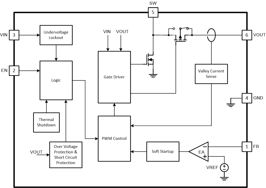
TPS61023 device is a synchronous boost converter with 0.5-V ultra-low input voltage. The device provides a power supply solution for portable equipment and smart devices powered by various batteries and super capacitors. The TPS61023 has typical 3.7-A valley switch current limit over full temperature range. With a wide input voltage range of 0.5 V to 5.5 V, the TPS61023 supports super capacitor backup power applications, which may deeply discharge the super capacitor.
The TPS61023 operates at 1-MHz switching frequency when the input voltage is above 1.5 V. The switching frequency decreases gradually to 0.5 MHz when the input voltage is below 1.5 V down to 1 V. The TPS61023 enters power-save mode at light load condition to maintain high efficiency over the entire load current range. The TPS61023 consumes a 20-µA quiescent current from VOUT in light load condition. During shutdown, the TPS61023 is completely disconnected from the input power and only consumes a 0.1-µA current to achieve long battery life. The TPS61023 has 5.7-V output overvoltage protection, output short circuit protection, and thermal shutdown protection.
The TPS61023 offers a very small solution size with 1.2-mm×1.6-mm SOT563 (DRL) package and minimum amount of external components.
Features
Input voltage range: 0.5V to 5.5V
1.8V Minimum input voltage for start-up
Output voltage setting range: 2.2V to 5.5V
Two 47mΩ (LS) / 68mΩ (HS) MOSFETs
3.7A Valley switching current limit
94% Efficiency at VIN = 3.6V, VOUT = 5V and IOUT = 1.5A
1MHz Switching frequency when VIN > 1.5V and 0.5MHz switching frequency when VIN < 1V
Typical 0.1µA shutdown current from VIN and SW
±2.5% Reference voltage accuracy over -40°C to +125°C
Auto PFM operation mode at light load
Pass-through mode when VIN > VOUT
True disconnection between input and output during shutdown
Output overvoltage and thermal shutdown protection
In the previous articles, we discussed that the digital logic uses Boolean data type which comprises of only two states i.e. “0” and “1”, and which are also referred to as “LOW” and “HIGH” states, respectively. The set of rules and laws can be applied to Boolean data types to find the optimum solution. As such, a digital logic circuit can be expressed in a Boolean Algebraic equation, and, by applying Boolean rules, laws, and theorems on this equation, an optimum digital circuit can be deduced. This optimum digital circuit benefits reduced logic, size, power consumption, and cost. Augustus DeMorgan, an English Mathematician, gave two famous laws known as DeMorgan’s Theorems which imparted a major contribution to Boolean Algebra. DeMorgan’s Theorems will be explained later in this article. However, in simple words, DeMorgan’s Theorems can be used to find the equivalency of NAND and NOR gates by viewing these operations as separate NOT-AND and NOT-OR functions, respectively.
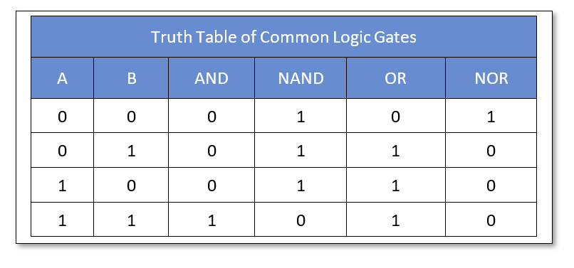
The truth table comprising of AND, NAND, OR, and NOR logic functions against two inputs is given below. These logical functions are used in DeMorgan’s Theorems and, as such, given to recall these logical operations.
The above given logical functions are denoted by equivalent Boolean notations. A “.” between operands means AND (Multiplication) operation, a “+” means OR (Sum) operation, and overline means an inversion of the operand. The equivalent Boolean notations of commonly used logical functions are shown in the following table.
DeMorgan’s Theory
DeMorgan’s Theory states two sets of laws or rules which are applicable to Boolean expressions having AND, OR, and NOT logical operations with two inputs (or more). Using these theorems, the logical operation of two variables is negated and converted into another logical operation. Such as, the logical NOR operation on two (or more) variables is equivalent to inversion of these variables and AND’ed together. Similarly, the logical NAND operation on two (or more) variables is equivalent to inversion of these variables and OR’ed, together. In other words, using DeMorgan’s theorems, the AND operator is replaced with the OR operator, and the OR operator is replaced with the AND operator.
DeMorgan’s First Theorem
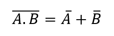
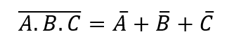
According to DeMorgan’s First Theorem, the resultant of two (or more) variables AND’ed and inverted (NOT) as a whole is equivalent to the OR of the complements of individual variables. Thus, AND + NOT (NAND) operation on variables is equivalent to the sum (OR) of the individual complement of each variable. In Boolean expression, it is stated as follow:
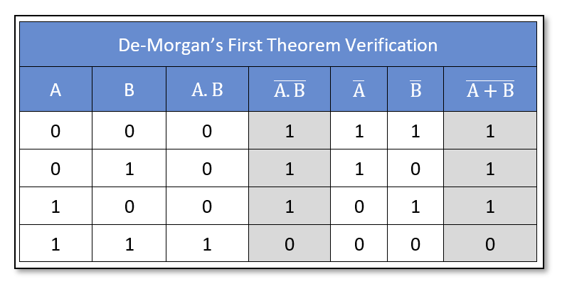
Verification of DeMorgan’s First Theorem using Truth Table
DeMorgan’s First Theorem can be verified using a truth table as illustrated below:
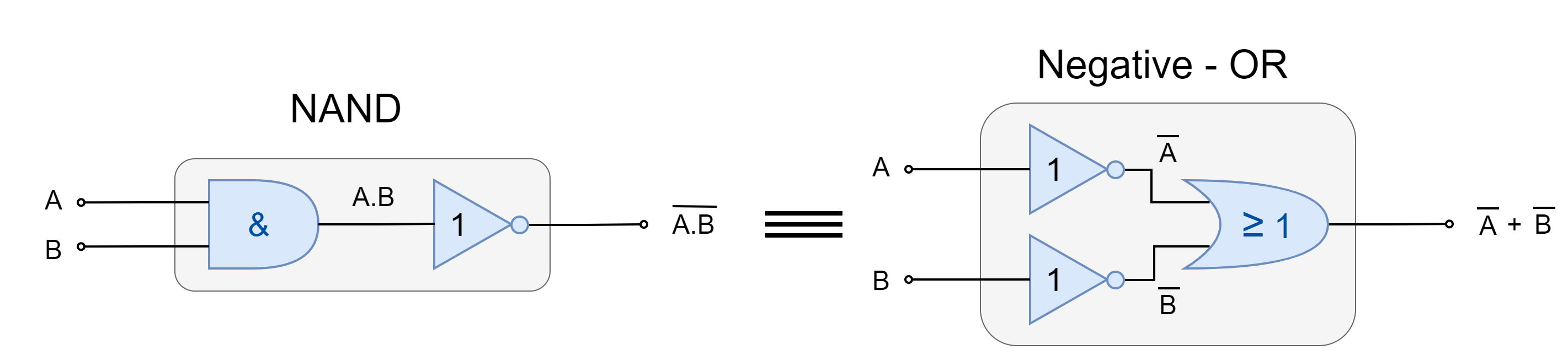
DeMorgan’s First Law Implementation
The following figure shows the implementation of DeMorgan’s First Theorem. The two logic circuits are equivalent to each other as per DeMorgan’s First Theorem.
Figure 1: Implementation of DeMorgan’s First Theorem
The left logic circuit forms a NAND (AND + NOT) gate. Whereas the right logic circuit, first inverts the inputs then they are OR’ed. These two logic circuits are equivalent to each other i.e. NAND = negative-OR. It can also be stated that a complement can be shifted from the output of the AND gate to the individual input of an OR gate and will be identical in logic operation as per the first theorem of DeMorgan.
DeMorgan’s Second Theorem
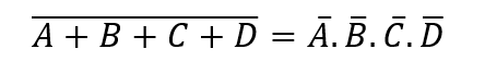
According to DeMorgan’s Second Theorem, the resultant of two (or more) variables OR’ed and inverted (NOT) as a whole is equivalent to the AND of the complements of individual variables. Thus, OR + NOT (NOR) operation on variables is equivalent to AND of the individual complement of each variable. In Boolean expression, it is stated as follow:
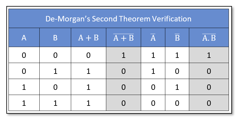
Verification of DeMorgan’s Second Theorem using Truth Table
DeMorgan’s Second Theorem can be verified using a truth table as illustrated below:
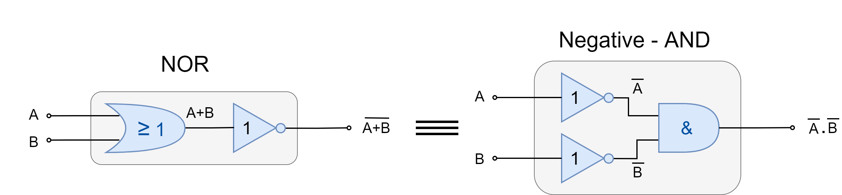
DeMorgan’s Second Law Implementation
The following figure shows an implementation of DeMorgan’s Second Theorem. The two logic circuits are equivalent to each other as per DeMorgan’s Second Theorem.
Figure 2: Implementation of DeMorgan’s SecondTheorem
The left logic circuit forms a NOR (OR + NOT) gate. Whereas the right logic circuit, first inverts the inputs then they are AND’ed. These two logic circuits are equivalent to each other i.e. NOR = negative-AND. It can also be stated that a complement can be shifted from the output of OR gate to individual input of an AND gate and will be identical in logic operation as per the second theorem of DeMorgan.
Thus, according to DeMorgan, an AND operation on inverted inputs is equivalent to NOR (OR + NOT) operation and vice versa. Similarly, an OR operation on inverted inputs is equivalent to NAND (AND + NOT) operation and vice versa.
In the above text, DeMorgan’s theorems have been applied to two-input variables. However, theorems are equally valid for more than two inputs variables.
For three-input variables:
DeMorgan’s First Theorem:
DeMorgan’s Second Theorem:
For four-input variables:
DeMorgan’s First Theorem:
DeMorgan’s Second Theorem:
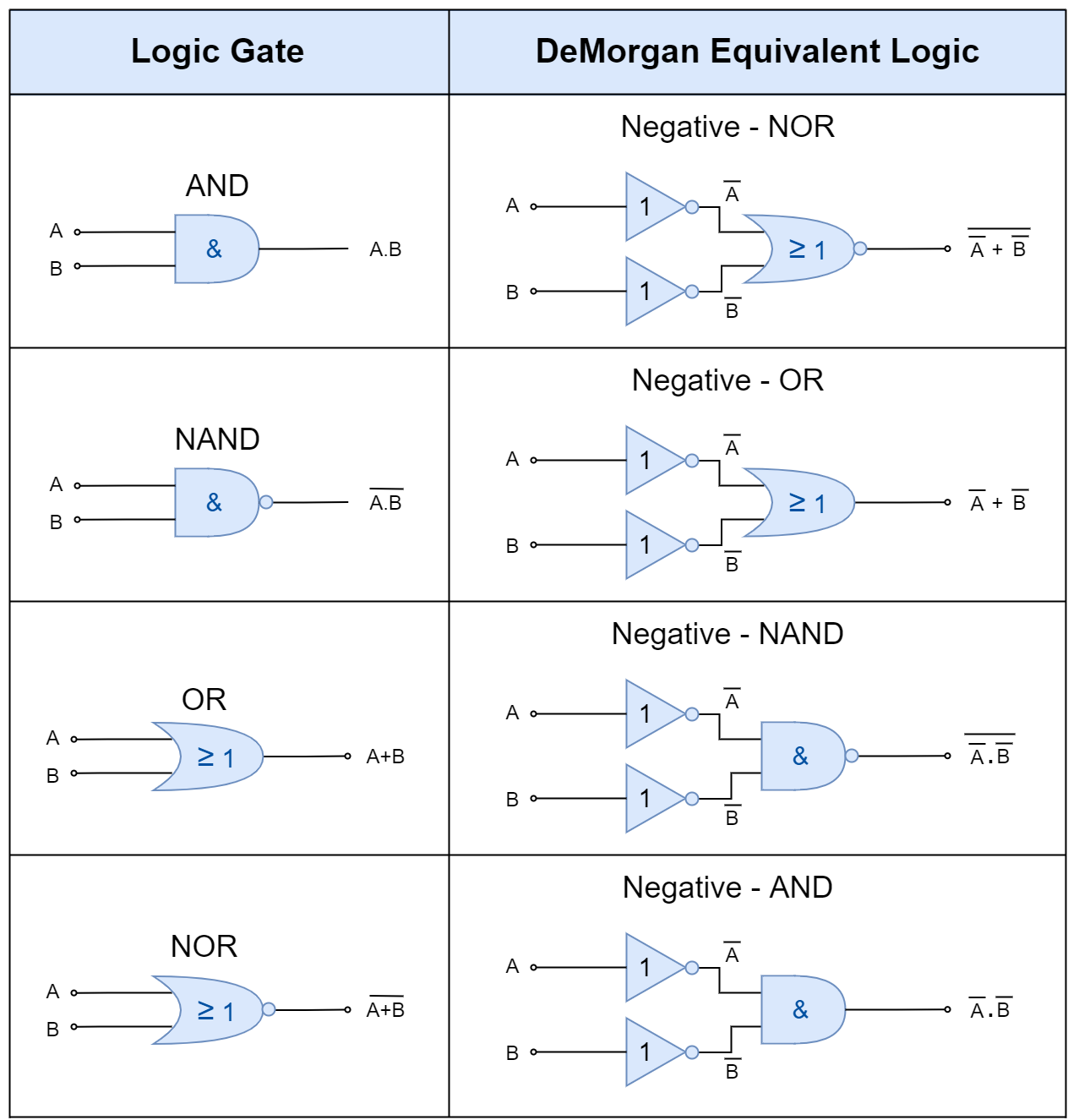
DeMorgan’s Equivalent Gates
The standard logic gates i.e. AND, NAND, OR, and NOR representing DeMorgan’s theorems can be obtained. It has already been discussed above that the NAND (AND + NOT) operation can be replaced by the OR logic on inverted inputs. Here, firstly, AND logic is replaced with the OR, and, secondly, the inversion is applied at the inputs and outputs. Resultantly, the AND + NOT logic becomes NOT + OR. The inputs which were originally not inverted become inverted and inverted output becomes non-inverted. The same can be applied to DeMorgan’s Second Theorem to obtain equivalent logic gates.
The following table shows the standard equivalent logic gates of DeMorgan’s theorems.
Conclusion
Augustus DeMorgan, an English Mathematician, gave two famous laws known as DeMorgan’s Theorems which are used to find the equivalency of the NAND and NOR logic gates.
DeMorgan’s First Theorem states that the NAND gate can be replaced with the OR function having inverted inputs i.e. Invert-OR logic.
DeMorgan’s Second Theorem states that the NOR gate can be replaced with the AND function having inverted inputs i.e. Invert-AND logic.
According to DeMorgan’s theorems, the AND logic can be replaced with the OR logic with inversion applied at the inputs and the output. Similarly, the OR logic can be replaced with the AND logic with inversion applied at the inputs and the output.
The AND logic can be replaced with the Inversion-NOR logic.
The NAND logic can be replaced with the Inversion-OR logic.
The OR logic can be replaced with the Inversion-NAND logic.
The NOR logic can be replaced with the Inversion-AND logic.
This project will turn your PyPortal into an MP3 player to play your favorite tunes with the familiar Winamp look. Create and manage multiple JSON playlists and rock out to whichever one fits the mood.
Take it a step further by choosing a custom Winamp skin and converting it for use on your PyPortal.
The Knowles AISonic audio edge processor IA8201 is a high-performance, ultra-low-power audio-centric OpenDSP supporting up to 4 mics, multiple high-speed interfaces, and GPIOs in two package options (eWLB and QFN). It provides low power, high efficiency, privacy, and compute power enabling customers to design modern products with far-field voice processing functionality for accurate listening. The IA8201 enables wake-on-voice processing for low latency voice UI, noise reduction, context awareness, and accelerated machine learning inferencing for edge processing of sensor inputs.
Knowles currently utilizes a modular approach to add voice with the capability to work with existing platforms and MCUs. IA8201 allows easy integration with legacy MCU system boards by running these commands over a simple UART interface.
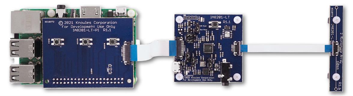
The IA8201-RDI-01 is an evaluation kit based on the Knowles AISonic audio edge processor IA8201. It is a complete system-level solution that enables Knowles customers to quickly go from an idea to a front-end audio solution that meets their platform requirements. It includes an IA8201-LT dev board, Raspberry Pi connector board, one 3-mic array, one 2-mic array, and flex cable connectors. The system firmware release to connect this platform is available on solution.knowles.com. It also comes with support of Sensory Voice Hub, which allows a user to create wake-words and local commands using a Web-based voice user interface.
Use Case Examples
Low power voice wake: Listens for specific OEM keywords to wake the host processor. Large memory enables processing of multiple stages on-chip for accurate results.
Proximity detection: When combined with an ultrasonic capable speaker and microphone, detects the distance between the system and an object; can replace an IR-Prox sensor in bezel-less phones.
Hub: Determines location of voice source while tuning out a noisy environment and lowering music to detect voice commands. Simultaneously takes metadata input and overrides beamformer to focus on camera-tracked objects.
Security system: Activate with a voice command. Detect glass breakage/smoke alarm, log direction of noise source, trigger alarm, and send alerts through Wi-Fi connection.
Wireless earbuds: Delivers low power premium wake-on-voice performance, talk detection to eliminate false triggers, enhanced voice quality through advanced beamforming and noise reduction algorithms, and support for local commands, including answer/ignore calls.
Features
Multi-Core: DeltaMax, optimized for compute; HemiDelta, optimized for low power
Audio interfaces: Up to 4x PDM digital microphones – 1 stereo inputs, 4 x mono inputs, and 1 stereo output, supporting clock rates up to 6.144 MHz; up to 3x PS/TDM ports supporting 8 channels each of 32-bit audio data using a 24.576 MHz input clock
Control interfaces: SPI, I2C, UART, available GPIOs
Memory: 1.44 MB RAM (1 MB available to users)
Clock: 175 MHz
Packaging options: eWLB 3.00 mm x 2.6 mm x 0.715 mm, 0.4 pitch, 42 ball; QFN 6.00 mm x 6.00 mm x 0.75 mm, 0.5 pitch, 40 lead
System requirements: IA8201BC 1.8 VDD, IA8201CQ 1.8 VDD and 3.3 VDD, -20°C to +85°C
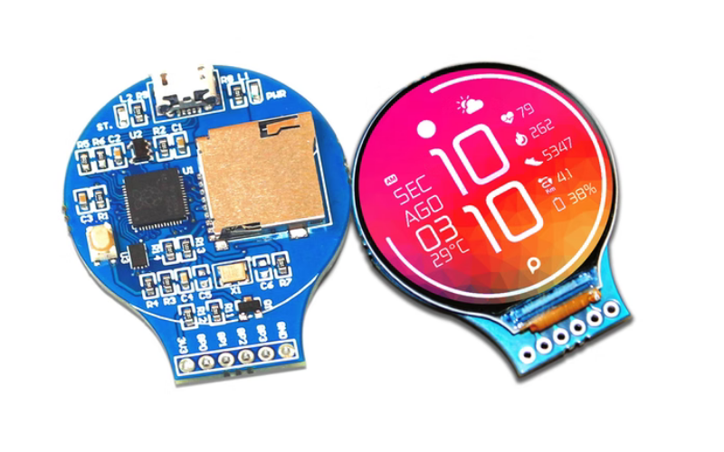
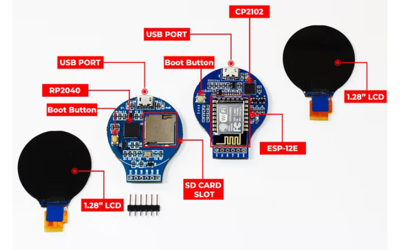
UK-based hardware developer Om Singh has launched a crowdfunding project built on two popular microcontrollers, RP2040 and ESP32. The RoundyPi, as the name suggests, is a Raspberry Pi’s in-house silicon tape-out RP2040 powered, compact and stylish LCD display of size 1.28-inches. RP2040 brings its distinctive characteristics of high performance, low cost, and ease of use to the microcontroller space. With a display of a 1.28-inch color screen and a resolution of 240×240 pixels, as well as an SD card slot, USB port, and the GC9A01 driver, bring down the number of I/O pins required. RoundyPi features two USB ports, one for power transmission and the other for data transmission, and provides one slot for an SD card.
The high-performance MCU RP2040 is quite flexible and versatile with digital screens that deliver remarkable efficiency and power for petite and compact dimensions. It incorporates a minimal-power ARM dual-core Cortex-M0+ processor with a CPU speed of up to 133MHz. Furthermore, the RP2040 features 264KB on-chip RAM, a DMA controller, two UARTs, two SPI controllers, and two I2C controllers, which together enable the module to run efficiently and quickly. Among the most appealing features of this low-cost microcontroller is the incorporation of a potentially powerful chip, the RP2040, at an unbeatable price, which will help clients construct cost-effective embedded electronics components or projects.
Another product, RoundyFi, based on the ESP-12E is a circular LCD with an elegant and sleek display unit of the same size as RoundyPi of 1.28 inches with 240×240 resolution and 65K RGB colors. It offers a vivid and vibrant effect that will enhance and boost the project’s user interface. Featuring an inbuilt GC9A01 driver and an SPI interface, RoundyFi considerably reduces the number of I/O pins required. Circular-shaped LCD displays have gotten trendy recently as they offer the project a modest and impressive appeal, which is often quite aesthetically pleasing.
Wireless power network provider, Energous Corporation, has revealed its association with Syntiant, to develop Energous’ WattUp wireless power network technology with Syntiant’s Neural Decision Processors (NDPs) for edge artificial intelligence deployments across a wide range of consumer and industrial use cases.
Syntiant, the California-based tech company, integrates the “most efficient silicon with a data platform and a training pipeline”, thereby furnishing its users with low-cost and turn-key solutions that embed deep learning processing in almost any edge device, ensuring privacy and security while avoiding cloud connectivity. From earbuds, medical gadgets, smart home appliances to industrial IoT equipment, and vehicles all avail the usage of Syntiant’s ultra-low-power NDPs. Syntiant’s AI processors furnish 100x more performance and 10x the throughput relative to current reduced power microcontroller unit solutions, owing to a clean-sheet, hardware/software co-design approach.
“Syntiant’s Neural Decision Processors help reduce infrastructure costs by moving AI processing from the cloud to the edge, reliably, securely and with nominal power consumption”, said CEO of Syntiant, Kurt Busch.
“We share a similar perspective with Energous that much of tomorrow’s innovation is happening at the edge, and our collaboration will successfully demonstrate both technologies working together, delivering power where it is not while providing highly accurate, cloud-free inference across a wide range of consumer and industrial applications.”
Energous includes a WattUp PewerBridge transmitter that discharges conducted radio frequency power in a determined arena or direction, unlike passive solutions that garner energy from the neighboring environment, which tends to offer incredibly low amounts of power and can be inherently uncertain about how much power is accessible. The receiving devices, then gather this RF-based energy. Extending improvements in power, efficiency, foreign device detection, freedom of movement, and the overall cost is the main aim behind the positioning of WattUp. It is built on fast, efficient, and highly scalable RF-based charging technology.
Energous wireless power networks provide “one to many” charging, which means that a single transmitter can charge numerous devices at the same time. It can be used in a variety of industries and applications, including medical, storage, monitors, and patient trackers in healthcare, smoke detectors and motion sensors in smart homes, and defect prevention, temperature, and other safety sensors in industrial settings.
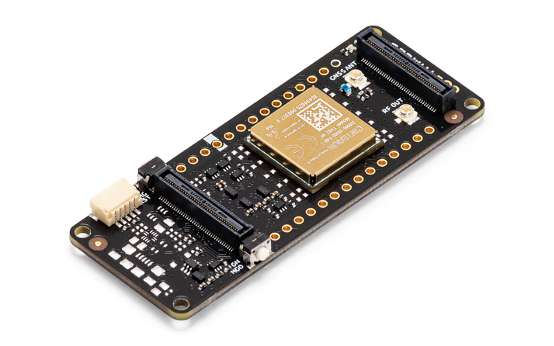
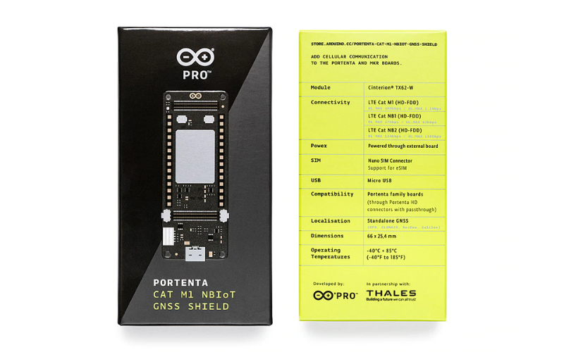
The Portenta Cat. M1/NB IoT GNSS Shield is Arduino’s latest embedded electronic hardware product developed in partnership with aerospace, defense, transportation, and security multinational Thales. The hardware offers rich connectivity attributes of the Portenta H7 applications. The GNSS shield helps liberate an exciting sphere of opportunities for edge computing.
The Portenta Cat. M1/NB IoT GNSS Shield delivers optimized bandwidth and performance while bringing global connectivity and positioning capabilities to Portenta and MKR boards by employing a Cinterion TX62 wireless module engineered for super-efficient, minimal power IoT applications.
Working in conjunction with Portenta H7’s strong edge computing capabilities, the Portenta Cat. M1/NB IoT GNSS shield facilitates asset tracking and remote monitoring solutions in industrial settings, agriculture, public utilities, and smart cities. With the ability to use eSIM technology, the shield provides cellular connectivity to both Cat.M1 and NB-IoT networks. With GPS, GLONASS, Galileo, or BeiDou, you can effectively monitor your belongings all through the city or across the globe.
Specifications of Portenta Cat. M1/NB IoT GNSS Shield
The shield facilitates embedded IPv4 and IPv6 TCP/IP stack access. The Portenta Cat. M1/NB IoT GNSS Shield has dimensions of 66×25.4 mm, which operates at temperatures of -40℃ to 85℃. Furthermore, it offers internet services which encompass TCP server/client, UDP client, DNS, Ping, HTTP client, FTP client, MQTT client Secure Connection with TLS/DTLS Secure boot.
Another key advantage of the shield includes changing the connectivity capabilities without having to change the board. Additionally, it is possible to create a small multi-protocol router (Wi-Fi – BT + NB-IoT/CAT.M1). This low-power module greatly reduces communication bandwidth requirements in IoT applications and is compatible with MKR boards.
For more information on the shield and to enhance your Portenta boards with cellular communication and positioning, kindly visit the Arduino Store.
MIPI Alliance has just announced the launch of the latest MIPI CSI-2 v4.0 interface. It adds features for environmental monitoring, multi-pixel compression and RAW28 color depth for safety-critical applications. Before understanding v4.0, let’s take a look at what MIPI CSI-2 is and its existing versions.
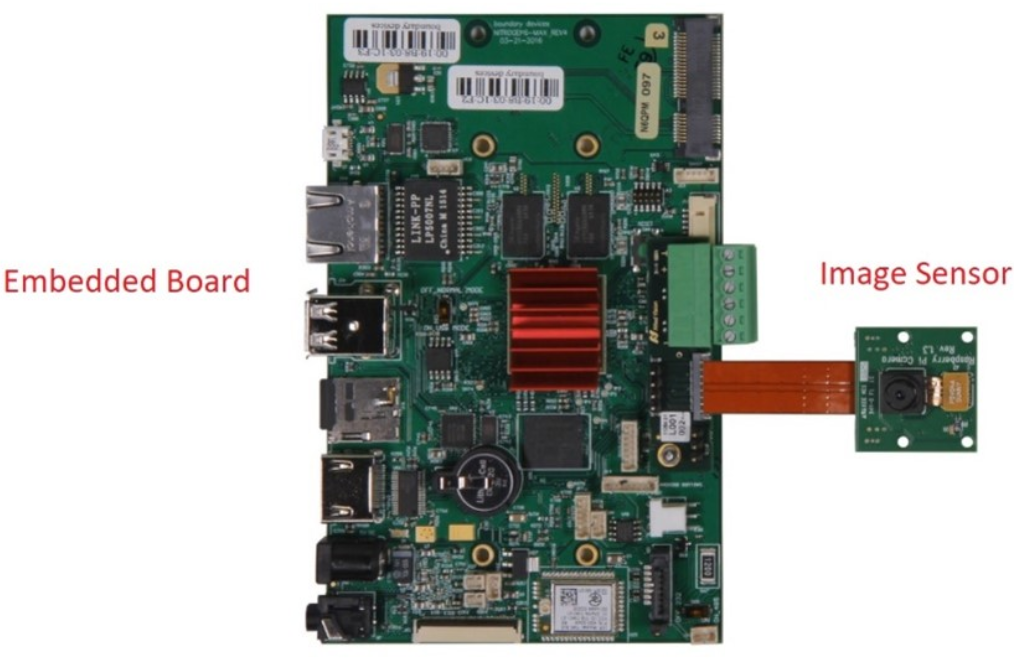
MIPI CSI-2 is a camera interface that connects an image sensor with an embedded board to control and process the image data. This helps the sensor and embedded board to act together like a camera system to capture images.
How does CSI-2 Protocol Work?
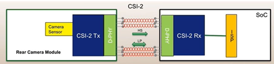
In a computer vision application, the image sensor captures and transmits an image to the CSI-2 host processor/SoC. The image is placed in the memory as individual frames. Each image frame is broken down into packets that include data format and error correction code (ECC) functionality. A single packet travels through the D-PHY layer and is split further according to the number of virtual channels. On the receiver end, the receiver is provided with a D-PHY physical layer for image extraction and error correction.
CSI-2 Protocol Timeline and Features
CSI-2 offers a maximum bandwidth of 6 Gbps, with an attainable bandwidth of 5 Gbps. MIPI CSI-2 supports high-resolution imaging. It can easily transmit images and videos in 1080p, 4K, and 8K formats. It is suited for both single and multi-camera implementations.
The MIPI CSI-2 v1.0 specification was released in 2005. MIPI CSI-2 is divided into the following layers: Physical Layer (C-PHY/D-PHY), Lane Merger Layer, Low-Level Protocol Layer, Pixel to Byte Conversion Layer and Application Layer
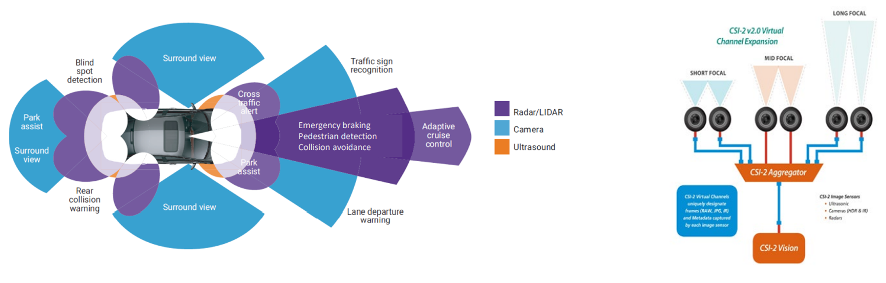
In April 2017, the CSI-2 v2.0 specification was released. It brought support for RAW-16 and RAW-20 color depth, increased virtual channels from 4 to 32, Latency Reduction and Transport Efficiency (LRTE), Differential Pulse-Code Modulation (DPCM) compression and scrambling to reduce Power Spectral Density.
RAW is the format of the image captured by the sensor without any processing. 16 or 20 is basically the number of bits per channel. Ex – An 8-bit camera can capture 2^8=256 different tonal values, by permutation and combination in each of the Red, Green and Blue channels. That makes a total of 256 X 256 X 256 = 16.7 million colors. Hence, in simple terms, MIPI CSI-2 v2.0 has the ability to transmit RAW-16 or 20 images to the CSI-2 host as per industry requirements.
Also, increasing the number of virtual channels from 4 to 32 augments the image transmission capabilities as a higher number of packets can be transmitted at the same time. This and Latency Reduction and Transport Efficiency (LRTE), Differential Pulse-Code Modulation (DPCM) compression makes CSI-2 v2.0 especially useful for use cases like Advanced Driver Assistance Systems (ADAS). CSI-2 v2.0 features are literally suited to transmit different inputs from multiple sensors with varying ranges and intensity.
MIPI CSI-2 v3.0 was released in 2019 and came with support for RAW-24 color depth.
CSI-2 v4.0 – More with less
Building on the machine awareness capabilities introduced in MIPI CSI-2 v3.0, v4.0 adds features to reduce lower power consumption, bandwidth demand and hence improving the ability to process better quality image input.
MIPI CSI-2 v4.0 is the first to support transmission of CSI-2 image frames over the low-cost, low-pin-count MIPI I3C/I3C basic two-wire interface. Some of the new features introduced by MIPI CSI-2 v4.0 are AOSC, Multiple-Pixel compression(MPC) and RAW-28 pixel encoding. Just like RAW 16 or 24, RAW 28 is the new pixel encoding supported by MIPI CSI-2 v4.0 for transmission of images of greater HDR to the processor for safety-critical operations like ADAS.
Another very important enhancement is the Always-On Sentinel Conduit or AOSC. This enables the image frame streaming from image sensor to VSP over a low-power MIPI I3C bus. This enables monitoring of the surrounding and triggers the host CPUs only when significant events happen, to save power.
Another important feature is the MPC or Multi-pixel compression. MPC reduces the bandwidth demand by compressing multi-pixel and standard Bayer CFA images with better efficiency. Hence, you can use the latest image sensors with high HDR image output without proportionally increasing the bandwidth.
To top it all off, CSI-2 v4.0 is backward-compatible with all previous versions of the MIPI specification.
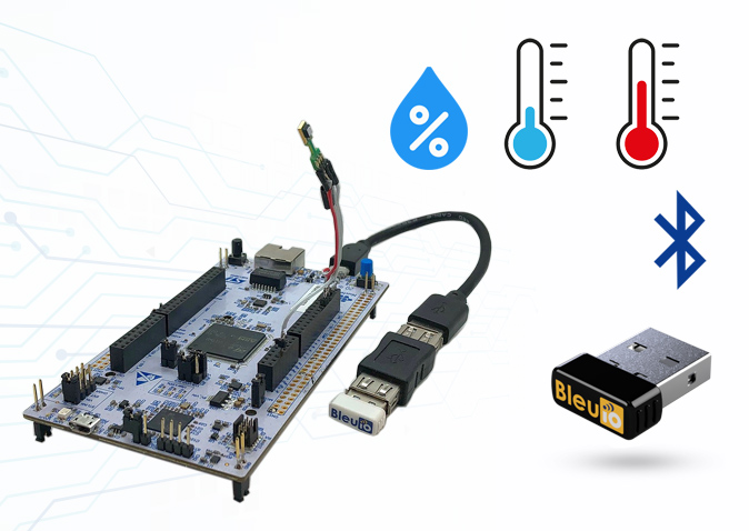
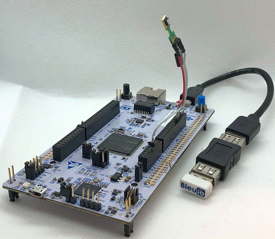
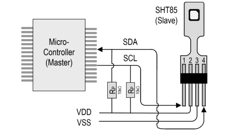
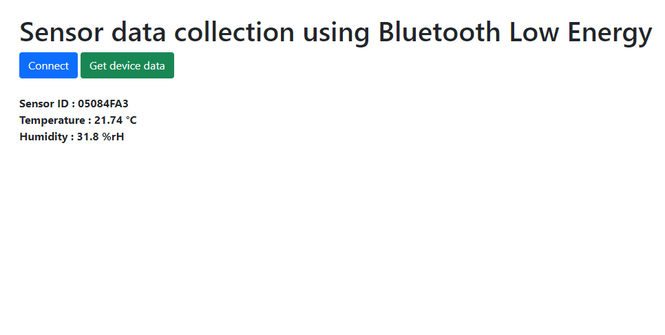
When the BleuIO Dongle is connected to the Nucleo board’s USB port, the STM32 will recognize it and start advertising the sensor values that it reads from the SHT85 along with the sensor serial number. It will update these values every 10 seconds.
Either clone the project or download it as a zip file and unzip it, into your STM32CubeIDE workspace.
Part 2 : Importing as an Existing Project
From STM32CubeIDE choose File>Import…
Then choose General>Existing Projects into Workspace then click ‘Next >’
Make sure you’ve chosen your workspace in ‘Select root directory:’
You should see the project “stm32_bleuio_SHT85_example”, check it, and click ‘Finish’.
If you download the project as a zip file you will need to rename the project folder from ‘stm32_bleuio_SHT85_example-master’ to ‘stm32_bleuio_SHT85_example’
Running the example
In STMCubeIDE click the hammer icon to build the project.
Open up the ‘STMicroelectronics STLink Virtual COM Port’ with a serial terminal emulation program like TeraTerm, Putty or CoolTerm.
In STMCubeIDE click the green play button to flash and run it on your board. The first time you click it the ‘Run Configuration’ window will appear. You can just leave it as is and click run.
Connect the BleuIO Dongle.
Access sensor data from a web browser
We wrote a simple script that connects to the BleuIO dongle and reads advertised data from STM32.
Create a simple Html file called index.html which will serve as the frontend of the script. This Html file contains some buttons that help connect and read advertised data from the remote dongle, which is connected to stm32.
Create a js file called script.js and include it at the bottom of the Html file. This js file uses the BleuIO js library to write AT commands and communicate with the other dongle.
import * as my_dongle from 'bleuio'

//connect to BleuIO
document.getElementById('connect').addEventListener('click', function(){
  my_dongle.at_connect()
})
//get sensor data
document.getElementById('getdata').addEventListener('click', function(){
  document.getElementById('loader').innerHTML = 'Loading'
  //set the BleuIO dongle into dual role
    my_dongle.at_dual().then(()=>{
      // sensor id of the device that we are trying to get data from
      let sensorID='05084FA3'

      //look for advertised data of with the sensor id
        my_dongle.at_findscandata(sensorID,4).then(x=>{

          //split the advertised data from the respnse
          let advdata= x[x.length-1].split(" ").pop()

          //trim the advertised string to only get sensor response
          const result = advdata.split(sensorID).slice(1).join(sensorID)

          //get temperature and humidity value
          let temp = result.substring(0, 4);
          let hum = result.substring(4, 8);

          //convert from hex to decimal and device by 100
          temp = parseInt(temp, 16)/100
          hum = (parseInt(hum, 16)/100).toFixed(1)

          document.getElementById('loader').innerHTML = ''
          document.getElementById('response').innerHTML = `Sensor ID : 05084FA3 <br/>
          Temperature : ${temp} °C<br/>
          Humidity : ${hum} %rH<br/>`
        })
    })

  })
The script js file has two button actions; connect and read advertised data.
We also need to update the Sensor ID on line 13 of script js. The Sensor ID of this example project is 05084FA3, which we got from SHT85.
Therefore this script looks for advertised data that contains sensor ID 05084FA3. After getting advertised data , we split the temperature and humidity information and show it on our index.html page.
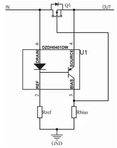
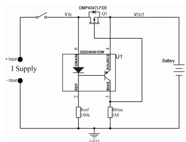
Diodes Incorporated DZDH0401DW Ideal Diode Controller is designed to drive a p-channel enhancement MOSFET configured as an ideal diode. This controller operates as a differential amplifier and PMOS controller to minimize forward current losses when VIN > VOUT. The DZDH0401DW controller provides high isolation when VIN < VOUT. This controller compares the voltage between input and output and if the differential is greater than ~34mV (typical), VBIAS will fall and PMOS will turn on. If the differential is less than ~70mV VBIAS will rise and the PMOS will turn off isolating the input from the output. The DZDH0401DW controller offers 40V maximum input voltage, -300mA peak bias current, 50V maximum reverse voltage protection, and comes in a SOT363 package. Typical applications include high side gate driving PMOS, high side disconnect switch, battery discharge protection, emergency lighting, and active OR’ing redundant power supplies.
Features
Drives a p-channel enhancement MOSFET configured as an ideal diode