MAX16163/MAX16164 nanoPower On/Off Controller

Maxim’s MAX16163 and MAX16164 nanoPower on/off controllers with programmable sleep time extend battery life up to 60%

Maxim’s MAX16163 and MAX16164 are nanoPower on/off controllers with programmable sleep time. The devices integrate a power switch to gate an output, which provides up to 200 mA load current.

The MAX16163 and MAX16164 use either an external resistor or an I2C bus to program the sleep time. When the device powers up, it checks the connection on the PB/SLP pin. If the resistance between the PB/SLP pin and ground is larger than 5.5 MΩ, the device is configured as I2C programmable. Otherwise, the device is configured as resistor programmable.

When the MAX16163 powers up, it measures the resistance on the PB/SLP pin to ground and sets the sleep time properly. It then asserts the OUT output. When the downstream device (e.g., a μC) finishes its task, it asserts a falling edge on the CLRB pin. The MAX16163 then deasserts OUT and the sleep timer starts. When the sleep timer expires, the MAX16163 asserts OUT again.

When the MAX16164 powers up, it measures the resistance on the PB/SLP pin to ground and sets the sleep time properly. It then keeps OUT deasserted and puts the device in shutdown state. The MAX16164 does not assert OUT until a pushbutton closure on the PB/SLP pin.

The MAX16163 and MAX16164 operate over the -40°C to +125°C temperature range and are available in a 1.54 mm x 1.11 mm, 6-bump thin wafer-level package (WLP) and a 6-pin μDFN package.

Block Diagram

Features

  • Ultra-low current saves power
    • 30nA IQ in sleep timer state
    • 10 nA IQ in shutdown state
    • VCC range: 1.7 V to 5.5 V
  • Robust features increase end equipment reliability
    • Pushbutton input handles up to ±60 V
    • ±40 kV HBM ESD protection
  • Flexible configurations provide design options
    • I2C or resistor programmable sleep time
    • Interrupt output and clear input in resistor programmable configuration
    • Up to 32 different sleep time values from 100 ms to 24 hours, and infinite
    • Latched output supplies 200 mA load current with less than 30 mV drop

more information: https://www.maximintegrated.com/en/products/power/power-management-ics/MAX16163.html

B&K Precision 5335C Single-Phase AC-DC Power Meters

B&K Precision 5335C Single-Phase AC-DC Power Meters measure and analyze power consumption and power quality parameters quickly and accurately. The 5335C supports power measurements up to 600VRMS and 20ARMS with a bandwidth up to 100kHz. Feature-rich measurement functions include all AC and DC parameters (power, current, voltage, power factor, frequency, and phase.) A powerful integration function performs harmonic measurements to the 50th order and an oscilloscope mode for viewing voltage and current reading in the time domain. Twelve real-time parameters can be measured and displayed simultaneously in user-customizable views.

Features

  • 600VRMS (Cat II) and 20ARMS direct input ranges
  • DC frequency range from 0.5Hz to 100kHz
  • 0.1% basic accuracy for voltage and current measurements
  • 4.3″ color LCD (TFT)
  • Simultaneously measure and display up to 12 measurement parameters
  • Capture inrush current and voltage surge with the peak function
  • Integration function with automatic range switching
  • Harmonic measurements to the 50th order
  • Ability to measure electrical energy which is produced or consumed
  • Pre-compliance testing according to IEC/EN 62000-3-2 / 4-7
  • Standard USB (USBTMC compliant), RS232, and LAN interfaces
  • Line and frequency filter capability for reducing unwanted signal noise
  • Optional universal breakout box to simplify the connection between the power meter and DUT

Specifications

  • 500Hz low-pass frequency filter
  • 600VRMS maximum common-mode input voltage
  • 2MΩ voltage input impedance +13pF in parallel
  • Maximum input voltage
    • 1.5kV-peak or 1kV-RMS continuous (whichever is less)
    • 2kV-peak or 1.5kV-RMS transient (whichever is less)
  • Temperature ranges
    • +5°C to +40°C operating
    • -20°C to +50°C storage
  • 20% to 80% relative humidity, non-condensing
  • 100VAC to 240VAC power, 50/60Hz
  • 50VAC maximum power consumption
  • Oscilloscope
    • 2-channel, voltage and current measurement
    • 10kHz bandwidth (-3dB)
    • 100kS/s sample rate
    • 1800V maximum input voltage
    • 60A maximum input current
  • 214.5mm x 88.2mm x 354.6mm in dimension (WxHxD)
  • 3-year warranty

more information: https://www.bkprecision.com/products/multimeters/5335B-power-meter.html

Noritake GTWQ043C3B00PWA 4.3″ TFT Touch Module

Noritake GTWQ043C3B00PWA 4.3″ TFT Touch Module is a wide operating temperature (-30°C to 85°C) model of a command-controlled touch TFT module. This module is designed to facilitate quick embedded GUI development and reduce system costs with powerful built-in commands. The GTWQ043C3B00PWA module has a 4.3″ diagonal screen size consisting of 480 x 272 pixels resolution with a high brightness of typical 850cd/m² capability. This module works with a 5V DC single power supply and 3.3V signal voltage. The GTWQ043C3B00PWA module features FLETAS® Metallized Projective Capacitive Touch (MPCT) screen that provides a wide range of touch sensitivity adjustments to perform adaptive sensitivity and noise-resistance. This module’s touch sensitivity is adjustable via simple commands over USB, I²C, SPI, and UART interfaces that will make an easier connection for most microcontrollers. The touch works with gloves and up to a 5mm acrylic overlay (with 0.5mm air-gap). The GTWQ043C3B00PWA module is ideally used in refrigeration, heating, and other industrial applications.

Features

  • -30°C to 85°C wide operating temperature range
  • 4.3″ TFT panel
  • FLETAS® Metallized Projective Capacitive Touch (MPCT) panel
  • 850cd/m2 high-brightness (typical)
  • 480 × 272 pixel resolution
  • 5V DC single power supply
  • Command-based operation makes GUI development quick and easy
  • Touch sensitivity is adjustable via simple commands over USB, I2C, SPI, and UART
  • On-board flash memory is available to store many images and fonts
  • RoHS compliant

more information: https://www.noritake-elec.com/news/product-release/new-wide-operating-temperature-4-3-tft-touch-module

EnSilica ENS62020 ultra-low power vital signs sensor interface IC for wearable healthcare and medical device markets

Supports accurate measurement of ECG, temperature, differential capacitance and optical signals. Integrates NFC energy harvesting circuit for optional battery-less functionality.

Ensilica has today announced the ENS62020, an ultra-low-power healthcare sensor interface IC for monitoring vital signs in wearable healthcare and medical devices.

The chip, which will be initially available with evaluation boards, has been created to meet the needs of a diverse array of home-use and single-use medical sensors – from oximeters to smart plasters – as well as wearable healthcare sensors and fitness trackers.

The IC is among the first of its kind to integrate an NFC energy harvesting circuit, making it suitable for both battery-powered and battery-less systems.

A modular IC design has been implemented in the ENS62020, which allows for the customisation of the ENS62020 and enables a product-optimised ASIC while greatly reducing the time to market.

EnSilica CEO, Ian Lankshear said:

“EnSilica is focused on developing ASICs in close collaboration with our customers. The ENS62020 was born out of requirements coming from a number of customers that were seeking to develop differentiated products in this fast-growing wearable healthcare and medical device market.”

The wearable medical sensors market is forecast to grow at 19% CAGR to 2024, with 280 million smart watches / fitness trackers and 160 million wearable medical sensors shipping in 2024 (source: Deloitte).

Block Diagram

Specifications

The ENS62020 healthcare sensor interface IC supports the accurate and reliable measurement of an array of vital signs. These include ECG, temperature and differential capacitance, as well as optical signals, which are used to track heart rate, oxygen saturation (SpO2), glucose levels and for near-infrared spectroscopy.

EnSilica has stated that due to the size and power-optimised design, the device is ideally suited to disposable medical devices and patches as well as sports and fitness devices. The highly sensitive capacitive sensor interface also makes the device well suited for novel MEMS sensors.

The IC is designed to work alongside an edge processor, or a communication device, and incorporates two photodiode drivers / photodetector readouts; two differential ECG sensor channels suitable for 3-lead ECG with <1.6µVrms noise levels; a highly sensitive capacitive sensor channel; a temperature sensor with <0.15oC resolution (between 35-45oC); a low-power ADC. The device consumes from just ~10µA per sensor.

Availability

The device will come in a plastic QFN 32-pin package, with samples available from June, or as part of an evaluation kit with board and demonstration software from July.

Further information on the chip is available via sales@ensilica.com

e-con Systems launches 4K HDR MIPI CSI-2 camera based on AR0821 for NVIDIA® Jetson Xavier™ NX / TX2 NX / Nano development kit.

High Dynamic Range | AR0821 | Large pixel size (1/2” sensor) | External hardware trigger

e-con Systems™, a leading embedded camera company has launched e-CAM81_CUNX, an 8MP (4K) HDR MIPI CSI-2 multi-board camera solution for NVIDIA® Jetson Xavier™ NX / TX2 NX / Nano development kit. This high-resolution camera is based on the latest AR0821 sensor from onsemi. The company had earlier launched See3CAM_CU81, a USB camera with the same sensor. It is the resounding success of this 4K HDR USB camera that led e-con Systems to extend this AR0821 camera module’s support to NVIDIA Jetson platforms.

Key features of e-CAM81_CUNX

  • High resolution – High resolution of 8 MP (4K) that helps to capture high-quality images with minuscule details.
  • MIPI CSI-2 interface – Compatible with the NVIDIA® Jetson Xavier™ NX / TX2 NX / Nano development kits.
  • Streaming resolution – HD and Full HD @ 30fps.
  • S-mount lens holder – Gives customers an opportunity to choose and use a lens of their choice.
  • High Signal to Noise Ratio (SNR) – Helps to achieve quality images with low noise even in poor lighting conditions
  • High Dynamic Range (HDR) – Helps to capture image data in challenging lighting conditions without any detail loss.

To learn how to evaluate e-CAM81_CUNX with the NVIDIA Jetson development kit, please watch the below video:

High resolution of 8 MP, MIPI CSI-2 interface, S-mount lens holder, HDR, and compatibility with NVIDIA® Jetson Xavier™ NX / TX2 NX / Nano development kits make this camera an ideal fit for applications such as kiosks, auto farming, retail automation, telepresence, document scanner, biometric & access control, parking lot management, sports broadcasting & analytics, smart traffic management, diagnostic devices, and life science & lab equipment.

Availability

Customers interested in evaluating e-CAM81_CUNX – 8MP (4K) HDR MIPI CSI-2 multi-board solution for NVIDIA® Jetson Xavier™ NX / TX2 NX / Nano development kit – can purchase the product from e-con Systems™’ online store. Please visit the e-CAM81_CUNX product page and click the buy now button to navigate to the webstore and purchase the product.

Customization and integration support

With a proper understanding of customers’ pain points, e-con Systems™ also offers customization services for e-CAM81_CUNX that reduce your efforts on prototyping, product integration, and product deployment. Please write to us at camerasolutions@e-consystems.com if you are looking for any customization or integration support.

Telematics for Electric Vehicles

Since 2019, The EV Market has taken great strides and is set to transform the automotive industry. Automotive OEMs have increased spend on R&D on electric models and sustainable technology.

Governments have introduced regulations and incentives to accelerate the shift to electric vehicles. Europe spearheaded this development, where EV adoption reached 8 percent due to policy mandates such as stricter emissions targets for OEMs and generous subsidies for consumers. Consumer attitude and increase awareness has led to a greater adoption of Electric Vehicles.

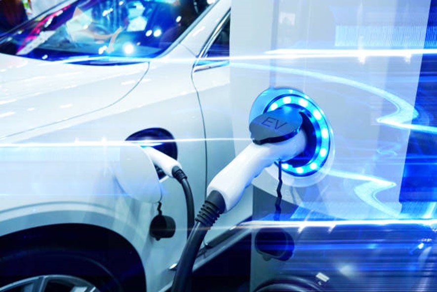
However, despite the promising trajectory of the EV market, some consumers have encountered challenges with their electric vehicles. From battery degradation to software glitches, a subset of buyers has faced frustrations that echo traditional automotive woes. Imagine eagerly embracing the future with the purchase or lease of a cutting-edge electric vehicle, only to be met with persistent issues that disrupt daily life.

In such cases, seeking recourse through legal avenues becomes necessary. Residents of California, in particular, benefit from robust consumer protection laws, including provisions for defective vehicles. Consulting a lemon law attorney in California can provide invaluable guidance and support for those grappling with the complexities of automobile malfunction and recourse. By navigating the legal landscape with expertise and diligence, these attorneys empower consumers to assert their rights and seek redress for their grievances, ensuring that the promise of electric mobility remains untarnished by individual setbacks.

In light of the challenges some electric vehicle owners may face, the role of expert auto repair services becomes increasingly crucial. Whether dealing with traditional internal combustion engines or cutting-edge electric powertrains, reliable maintenance and repair services are essential to keeping vehicles on the road. Blue Wrench Auto, a reputable establishment known for its commitment to excellence, stands ready to assist electric vehicle owners in resolving any issues they may encounter. With their specialized knowledge and state-of-the-art equipment, Blue Wrench technicians can diagnose and address a wide range of electric vehicle issues efficiently and effectively. With their assistance, electric vehicle owners can overcome obstacles and continue to enjoy the benefits of emission-free driving with confidence and peace of mind.

Amidst the evolving landscape of electric mobility, the role of infrastructure becomes paramount. While the focus often rests on the vehicles themselves, the availability and reliability of charging stations are equally crucial for seamless integration into daily life. A swift search for electrician near me can link residents to experts like Advantage Electric, who are licensed and contracted to install Electric Vehicle charging ports in homes and businesses across Minnesota. This convenient accessibility to skilled professionals ensures that the transition to electric driving is not impeded by logistical hurdles but instead facilitated by efficient and effective solutions.

Advantage Electric’s expertise transcends mere installation; they possess a deep understanding of electric vehicle charging systems, tailoring solutions to match the unique needs of each client. Their commitment to top-notch craftsmanship mirrors the ethos of the evolving electric vehicle market, where reliability and efficiency reign supreme. Through collaboration with esteemed partners like Advantage Electric, the aspiration for a sustainable, electrified future isn’t just a distant dream but rather finely tuned to meet the demands of contemporary consumers.

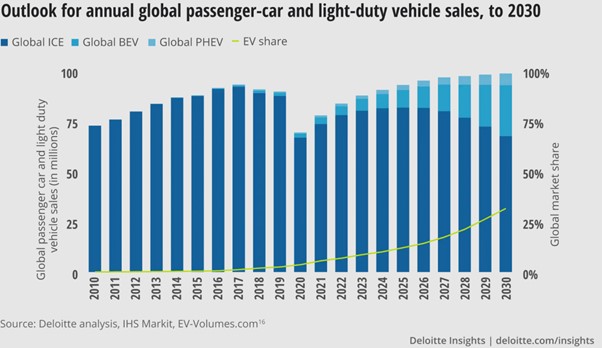
A Deloitte report suggests that the global EV markets is to grow with a CAGR of 29 per cent achieved over the next ten years: Total EV sales growing from 2.5 million in 2020 to 11.2 million in 2025, then reaching 31.1 million by 2030.

Benefits of Telematics for Electric Vehicles

  • Driving Experience: In Electric Vehicles, it is very important for the driver to know the range of the vehicle, know his next charging station and plan his trip accordingly. The Telematics unit can determine the location of the vehicle, and through mapping and information on the range and available chagrining infrastructure, can help pre book the charging spot at a location to save time.
  • Charging Analytics and EV Energy Usage: Telematics can help monitoring the charge level, battery health and provide valuable data required to improve the vehicle algorithms. Continuous updates and advancements on charging time, battery size and weight are being taken up by EV manufacturers. The real time data provides the manufacturers with a rich data source for their development and analytics. Such analytics can also help notify on the battery status of your vehicle.
  • Fleet Management and route mapping: A lot of last mile delivery trucks are now powered through batteries. Field service managers can work through an effective route management, benchmark vehicle utilization, monitor charge reporting, and measure whether their plans are effective in reducing costs and emissions.
  • Alerts and Notifications: The telematics units can determine the state of charge of the battery and alert the driver through an SMS on the need to find a chagrining spot immediately. Alerts such as an issue with the battery can be provided on real time to the driver to avoid troublesome situations on the road.
  • Firmware Update: With continuous advancements on the charging algorithms and software of an electric vehicle, the telematics unit can also act as a bridge for firmware update of the ECU and electronics within an electric vehicle. The telematics unit with LTE connectivity can be connected to a server for updates and an OTA update mechanism.

Successful EV Management with Telematics

  • Receive notifications when batteries reach critical status and is time to charge
  • Cost Reduction by planning of charging cycles based on the peak electricity rate times
  • Performance reporting and finding out impact and return on investment through electrification
  • Recharging priorities based on state of charge and operational schedules

Telematics Hardware for Electric Vehicles

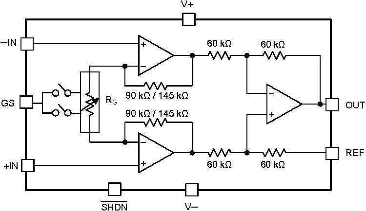
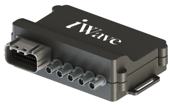
To connect to the electric vehicles, you can utilize a Telematics Control Unit or a gateway. Integrated with 3 CAN Ports and wireless technologies such as 4G, Wi-Fi and Bluetooth, a powerful telematics control unit is what can enable intelligence on an electric vehicle.

The provision for 3 CAN Ports makes the telematics control unit an ideal fit for electric vehicles. Different CAN ports can be connected to the different terminals within the EV Backbone to tap different data points on different CAN buses.

Unlike conventional vehicles, EVs do not follow mandatory telematics data standards, making data access a challenge. Hence, the LINUX powered telematics control unit provides the software flexibility and transparency to be compatible with different makes and models of electric vehicles.

The wireless technologies provide the capability to power different uses cases such as SMS alerts and notifications to the drivers and fleet owners. Wi-Fi can help in firmware update of the ECU and vehicle electronics when connected to your home networks and lay the foundation for the ever-evolving use cases.

EVs have unique metrics that need to be monitored to optimize their performance, range and return on investment, making telematics a must for electric vehicles.

Learn more at:

To get in touch with us for inquiries and further information, please write to mktg@iwavesystems.com or contact our Regional Partners.

Orbex Group Introduces Ultra-Small Pancake-style Gimbal Motors

Orbex Group has introduced a line of ultra-compact high-performance gimbal motors. Featuring a pancake-style form factor, the motors are wound to operate at low speeds typical for gimbals while exhibiting a high torque constant for fast response when needed.

The new gimbal motors are engineered to minimize cogging torque, ensuring smooth rotation for stable imaging or pointing. Because these brushless motors are electronically commutated, they can change speeds quickly and offer exceptional reliability. Orbex gimbal motors are also lightweight — an important characteristic for drones, UAVs and other airborne craft that need to maximize flight time.

Orbex gimbal motors are available in two sizes: 16 millimeters (OD) by 10 millimeters (H) and 26 millimeters (OD) by 12 millimeters (H). In addition to these standard units, Orbex can engineer your motor according to your application’s needs, with special windings, connector configurations or mounting interfaces. The motors also allow users to easily integrate a magnetic encoder for feedback.

For more information, visit www.orbexgroup.com.

INA350 – Tiny and low-power (100 µA) selectable gain instrumentation amplifier

INA350 is a selectable-gain instrumentation amplifier that offers four gain options across INA350ABS and INA350CDS variants available in small packages. INA350ABS has gain options of 10 or 20 and INA350CDS has gain options of 30 or 50. These gain options can be selected by toggling the gain select (GS) pin. INA350 is ideal for bridge-type sensing and for differential to single-ended conversion applications.

Built with precision matched integrated resistors, INA350 saves on BOM costs, pick-and-place machine handling costs, and board space by removing the need for precise or closely-matched external resistors. The device interface directly to low-speed, 10-bit to 14-bit, analog-to-digital converters (ADC) and is ideal for replacing the discrete implementation of instrumentation amplifiers built with commodity amplifiers and discrete resistors.

Designed with the three-amplifier architecture, INA350 is optimized for delivering performance. It achieves 85 dB of minimum CMRR and 0.6% of maximum gain error, along with 1.2 mV of maximum offset across all gain options, while consuming just 125 µA of maximum quiescent current. It has an integrated shutdown option to turn off the amplifier when idle for additional power savings in battery powered applications.

Features

  • Ideal for size, cost, and power conscious designs
  • Selectable gain options
    • G = 10 or G = 20 (INA350ABS)
    • G = 30 or G = 50 (INA350CDS)
  • Space saving ultra-small package options
    • 10-pin X2QFN (RUG) – 3 mm2
    • 8-pin WSON (DSG) – 4 mm2
    • 8-pin SOT23-THN (DDF) – 4.64 mm2
  • Optimized performance for 10-bit to 14-bit systems
    • CMRR: 95 dB (typ) across all gains
    • Offset voltage: 0.2 mV (typ) across all gains
    • Gain error (typ):
      • 0.05% for G = 10; 0.06% for G = 20
      • 0.075% for G = 30; 0.082% for G = 50
  • Bandwidth: 100 kHz for G = 10 (typ)
  • Drives 500 pF with less than 20% overshoot (typ)
  • Optimized quiescent current: 100 µA (typ)
  • Shutdown option for power conscious applications
  • Supply range: 1.8 V (±0.9 V) to 5.5 V (±2.75 V)
  • Specified temperature range: –40°C to 125°C

Block Diagram

more information: https://www.ti.com/product/INA350

Texas Instruments TPS61023 3A Boost Converters have input voltage as low as 0.5V

Texas Instruments TPS61023 3A Boost Converters provide a power supply solution for portable equipment and smart devices powered by various batteries and supercapacitors. The TPS61023 has a typical 3.7A valley switch current limit over a full temperature range and a 0.5V ultra-low input voltage. The TPS61023 supports supercapacitor backup power applications with a wide input voltage range of 0.5V to 5.5V, which may deeply discharge the supercapacitor.

The TPS61023 3A Boost Converters operate at 1MHz switching frequency when the input voltage is above 1.5V. The switching frequency decreases gradually to 0.5MHz when the input voltage is below 1.5V down to 1V. The TPS61023 enters power-save mode at light load conditions to maintain high efficiency over the entire load current range. The device consumes a 20µA quiescent current from VOUT in a light load condition.

During a shutdown, the TPS61023 is completely disconnected from the input power and only consumes a 0.1µA current, achieving a long battery life. The TPS61023 has 5.7V output overvoltage protection, output short circuit protection, and thermal shutdown protection.

Features

  • Input voltage range: 0.5V to 5.5V
  • 1.8V Minimum input voltage for start-up
  • Output voltage setting range: 2.2V to 5.5V
  • Two 47mΩ (LS) / 68mΩ (HS) MOSFETs
  • 3.7A Valley switching current limit
  • 94% Efficiency at VIN = 3.6V, VOUT = 5V and IOUT = 1.5A
  • 1MHz Switching frequency when VIN > 1.5V and 0.5MHz switching frequency when VIN < 1V
  • Typical 0.1µA shutdown current from VIN and SW
  • ±2.5% Reference voltage accuracy over -40°C to +125°C
  • Auto PFM operation mode at light load
  • Pass-through mode when VIN > VOUT
  • True disconnection between input and output during shutdown
  • Output overvoltage and thermal shutdown protection
  • Output short-circuit protection
  • 1.2mm × 1.6mm SOT563 (DRL) 6-pin package

Block Diagram

more information: https://www.ti.com/product/TPS61023

DFRobot 0.96″ 160×80 Color SPI TFT Display

DFRobot 0.96″ 160×80 Color SPI TFT Display employs an edge-to-edge design and offers a 160×80HD 16-bit color display. The display is suitable for wearable projects, mobile devices, and smart home products. It supports the DFRobot GDI display interface and can be conveniently connected to a GDI main-controller with FPC, plug, and play, and is easy to wire.

Features

  • TFT material, the better display effect
  • GDI interface, no soldering required
  • Narrower PCB, easy to be integrated into small projects
back side of the PCB

Layout

more information: https://www.dfrobot.com/product-2445.html

TOP PCB Companies