Texas Instruments TPS1HB08-Q1 Smart High-Side Switch

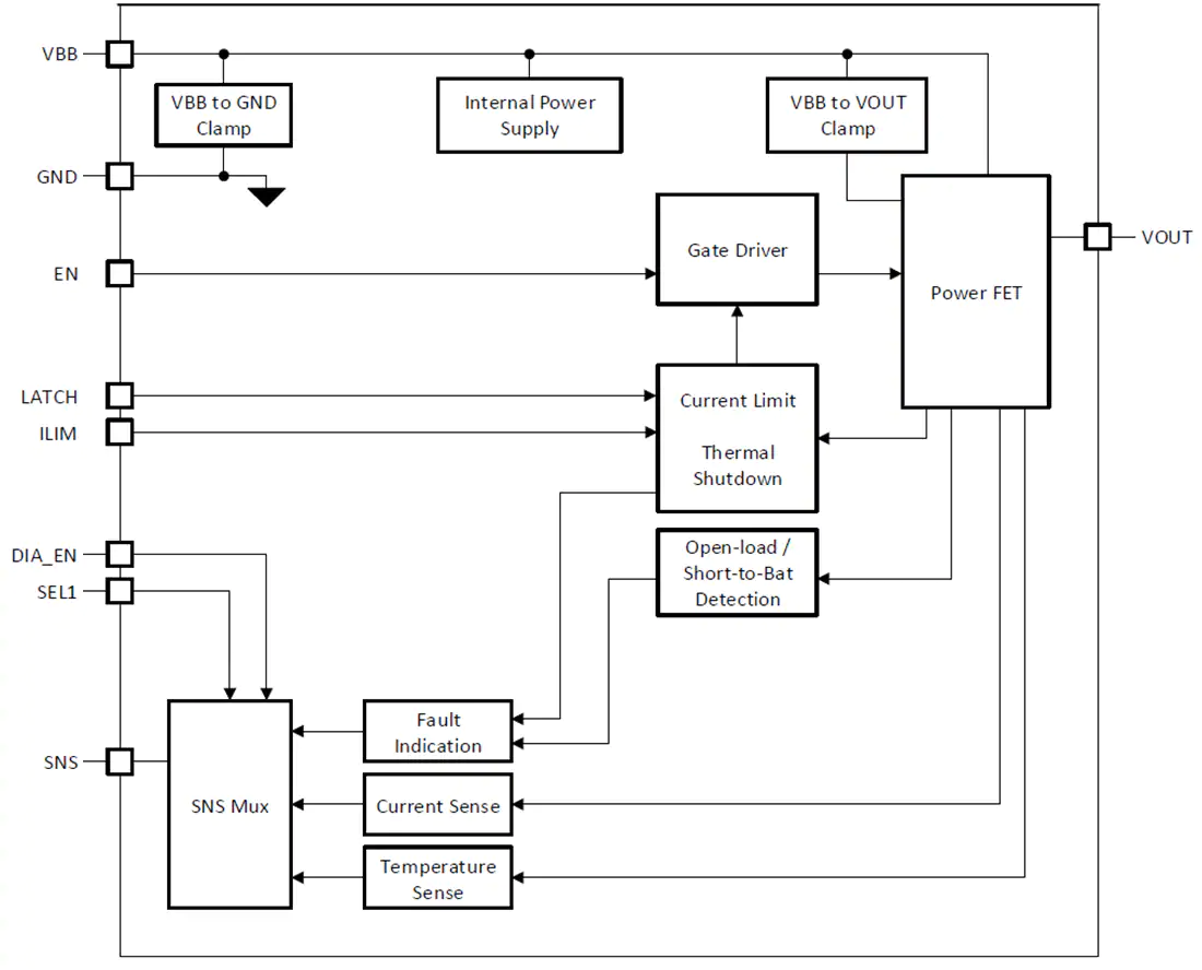
Texas Instruments TPS1HB08-Q1 Smart High-Side Switch is intended for use in 12V automotive systems. The device integrates robust protection and diagnostic features to ensure output port protection, even during harmful events like short circuits in automotive systems. The device protects against faults through a reliable current limit, which, depending on the device variant, is adjustable from 6.4A to 70A or set at 94A. The high current limit range allows for usage in loads that require large transient currents, while the low current limit range provides improved protection for loads that do not require high peak currents. The device is capable of reliably driving a wide range of load profiles.

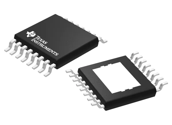
The TPS1HB08-Q1 also provides a high accuracy analog current sense that allows for improved load diagnostics. By reporting load current and device temperature to a system MCU, the device enables predictive maintenance and load diagnostics that improve the system lifetime. The TPS1HB08-Q1 is available in an HTSSOP package, which allows for a reduced PCB footprint.

Features

  • AEC-Q100 qualified for automotive applications
    • Temperature grade 1: –40°C to 125°C
    • Device HBM ESD classification level 2
    • Device CDM ESD classification level C4B
    • Withstands 40V load dump
  • Functional safety capable
    • Documentation available to aid functional safety system design
  • Single-channel smart high-side switch with 8mΩ RON (TJ = 25°C)
  • Improve system-level reliability through adjustable current limiting
    • Current limit set-point from 6.4A to 70A
    • Version F: 94A fixed ILIM
  • Robust integrated output protection
    • Integrated thermal protection
    • Protection against short to ground and battery
    • Protection against reverse battery events including automatic switch-on of FET with reverse voltage
    • Automatic shut off on loss of battery and ground
    • Integrated output clamp to demagnetize inductive loads
    • Configurable fault handling
  • Analog sense output can be configured to accurately measure
    • Load current
    • Device temperature
  • Provides fault indication through SNS pin or FLT pin
    • Detection of open load and short-to-battery

Block Diagram

more information: https://www.ti.com/product/TPS1HB08-Q1

TPSM63606 High-Density 6 A Power Module

Texas Instruments’ module is a highly-integrated 36 V DC/DC solution that comes in an enhanced HotRod™ QFN package

Texas Instruments’ TPSM63606 is a highly integrated 6 A, DC/DC synchronous buck power module that combines power MOSFETs, a shielded inductor, and passives in an enhanced HotRod QFN package. The module has pins for VIN and VOUT that are located at the corners of the package for optimized input and output capacitor layout placement. The four larger thermal pads beneath the module enable a simple layout and easy handling in manufacturing. With an output voltage range of 1 V to 16 V, the TPSM63606 is designed to quickly and easily implement a low-EMI design in a small PCB footprint. The total solution requires as few as four external components and eliminates the magnetics and compensation part selection from the design process.

Although designed for small size and simplicity in space-constrained applications, the TPSM63606 module offers many features for robust performance including precision enable with hysteresis for adjustable input voltage UVLO, resistor-programmable switch node slew rate, and a spread-spectrum option for improved EMI. The integrated VCC, bootstrap, and input capacitors provide increased reliability and higher density, constant switching frequency over the full load current range, and a PGOOD indicator for sequencing, fault protection, and output voltage monitoring.

Features

  • Functional safety-capable: documentation available to aid functional safety system design
  • Versatile 36 VIN, 6 AOUT synchronous buck module:
    • Integrated MOSFETs, an inductor, and a controller
    • Adjustable output voltage range: 1 V to 16 V
    • Package: 5.0 mm x 5.5 mm x 4 mm over-molded QFN
    • Junction temperature range: -40°C to +125°C
    • Adjustable frequency range: 200 kHz to 2.2 MHz
    • Negative output voltage capability
  • Ultra-high efficiency across the full load range:
    • Peak efficiency: 95%+
    • External bias option for improved efficiency
    • Shutdown quiescent current: 0.6 µA (typ.)
  • Ultra-low conducted and radiated EMI signatures:
    • Low-noise package with dual input paths and integrated capacitors reduces switch ringing
    • Spread-spectrum modulation (S-suffix)
    • Resistor-adjustable switch-node slew rate
    • Meets CISPR 11 and 32 Class B emissions
  • Suitable for scalable power supplies:
    • Pin-compatible with the TPSM63604 (36 V, 4 A)
  • Inherent protection features for robust design:
    • Precision enable input and open-drain PGOOD indicator for sequencing, control, and VIN UVLO
    • Overcurrent and thermal shutdown protection

more information: https://www.ti.com/product/TPSM63606

Analog Devices LT8333 Current-Mode DC-DC Converter

Analog Devices Inc. LT8333 Current-Mode DC-DC Converter integrates a 40V, 3A power switch and operates from a 2.8V to 40V input. With a unique single feedback pin architecture, this device is capable of Boost, SEPIC, or inverting configurations. Burst Mode® operation consumes as low as 9μA quiescent current to maintain high efficiency at very low output currents while keeping typical output ripple below 15mV.

The LT8333 operates over an input range of 2.8V to 40V, suitable for automotive, telecom, and industrial applications. The converter provides adjustable and synchronizable operation from 300kHz to 2MHz with the SSFM option. The LT8333 integrates other features such as programmable soft-start, bias pin, and input undervoltage lockout. The device can exhibit a low quiescent current down to 9μA in Burst Mode and 1μA in shutdown, making it ideal for battery-operated systems.

The Analog Devices Inc. LT8333 Current-Mode DC-DC Converter is available in a thermally enhanced 3mm x 3mm Dual Flat No-Leads (DFN) package with a -40°C to +150°C operating junction temperature range.

Features

  • Wide 2.8V to 40V input voltage range
  • Ultralow quiescent current and low ripple
  • Burst Mode operation: IQ = 9μA
  • 3A, 40V power switch
  • Positive or negative output voltage programming with a single feedback pin
  • Programmable 300kHz to 2MHz frequency range
  • Synchronizable to an external clock
  • Spread spectrum frequency modulation for low EMI
  • Bias pin for higher efficiency
  • Programmable undervoltage lockout (UVLO)
  • Overcurrent and overtemperature protection
  • Thermally enhanced 3mm x 3mm DFN-10 Package

Application Circuit

more information: https://www.analog.com/en/products/lt8333.html

High Current MOSFET Based Power Switch with Gate Driver

This power load switch project provides a simple and inexpensive method for power control. It is intended for driving a resistive or inductive load. A TTL logic signal from the system turns the load switch ON and OFF. The project consists of a low ohm N-Channel Power Trench MOSFET FDB0300N1007L and Gate driver MAX5048 chip.  The load can be controlled by applying a PWM signal or Logic input.

The MAX5048A is a high-speed MOSFET driver capable of sinking/sourcing 7.6A/1.3A peak currents. These devices take logic input signals and drive a large external MOSFET. The MAX5048A has noninverting inputs that give the user greater flexibility in controlling the MOSFET. They feature two separate outputs working in a complementary mode, offering flexibility in controlling both turn-on and turn-off switching speeds.

High Current MOSFET Based Power Switch with Gate Driver – [Link]

Single Key Touch Sensor using LM2907

This is a single key device featuring a touch ON (Momentary) output. The project is built using the LM2907 chip. The board provides stable sensing and has a wide working power supply range 5V to 12V DC and consumes 20mA. D1 power LED, D2 function LED.

Touch sensors are used in many applications, from remote controls, LED light controls to appliance control panels. This is a simple solution to replace a mechanical button and can be implemented in a wide variety of applications. The sensor provides a great user experience. It is easy and more convenient to use as it has no moving mechanical parts.

Single Key Touch Sensor using LM2907 – [Link]

End-to-End Circuit Testing Using Zoolark

Zoolark is a lean integrated implementation of Function Generators and Oscilloscopes. It is extremely handy for testing circuits without waiting in line for the high-end equipment at the lab.

The use of function generators and Oscilloscopes is to test circuits in an isolated environment. A function generator mimics the real expected input. Oscilloscope records the circuit output in a visual format.

Zoolark has it all, just smaller in size. It is an abstraction of useful features without the unnecessary high-end stuff.

Device Overview

Zoolark Physical Specifications

There are 5 modes: Function Generator, Oscilloscope, FFT, PWM, DC Offset. It has a Type-C USB port for charging/UART communication for debugging mode, a 3-way toggle to increment, decrement and confirm values, and a dedicated debugging port.

In Function Generator mode, Zoolark can mimic 3 input waveforms: Triangular, Square and Sinusoidal. It can generate frequencies in the range 0.1Hz to 1MHz. Amplitudes and DC Bias range from -4.0V to 4.0V. It has a DC impedance of 50 Ohm and the input signal to the circuit is in WAV format.

In Oscilloscope mode, Zoolark can record signals with a max peak-to-peak amplitude of 30V. It has a sampling rate of 5 Msps and analog bandwidth of 1 Mega Ohm. It has horizontal resolution with a time-base range from 50 microseconds to 50 seconds, vertical resolution with 50mV to 10V and CH1, CH2 ports for taking signal input.

Sampling Rate, or an average number of continuous signal span shots per second, is a very important parameter. The oscilloscope captures discrete snapshots of the continuous output signal and reconstructs the signal, up to the Nyquist limit. The number of signals it can capture is limited by the max sampling rate. The sampling rate for digital signals must be at least 4 times faster than their bandwidth. Similarly, it must be at least 10 times faster for analog signals. So make sure that you calculate the minimum sampling rate as per your requirement and check if it is lesser than the max sampling rate of the device.

In PWM mode, it can generate PWM signals with a voltage range of 0 to 3.3V, frequencies of 0.1Hz to 1MHz, duty cycle from 10% to 90%.

Developing on Zoolark

The microcontroller used for zoolark is STM32G491. Zoolark provides you the option to customize the UI of the device by programming and flashing the firmware.

Testing with Zoolark

Zoolark can be used to test circuits in various ways – input signals using function/PWM mode or capture output with Oscillator mode. You can probe an output signal on your PCB, DC Reference signal with custom precision, change the PWM duty cycle to adjust motor speed or sound decibel levels on speaker, or test LED configuration by generating various signals.

This concludes the article on Zoolark. Learn, build a circuit on a breadboard, connect zoolark to test out your LEDs or spin your motors. All you need is a table, a circuit and lots of interest.

For more details please visit this link

Valentine’s Day Large LED Heart PCB

A large heart with 20 individually controllable LEDS using 4 pins on an ATtiny 45 with Charlieplexing This is an easy to solder project, as all components are trough hole, except for the large and easy to solder battery holder Who would not like to be pledged eternal love to by their valentine giving them a large blinky LED heart Pendant!

“SaltyPaws” writes:

  • I developed this project, in order to introduce my daughters to electronics. This pendant can be used to introduce STEAM concepts at many levels. It can be used to introduce electronics, teach trough hole assembly/soldering and programming.
  • This is a basic demonstration of the Charlieplexing principle. The heart can be used stand alone or in a pendant.
  • I used FreeCAD in order to design the heart shape. Unfortunately at the time of designing, the offset tool was not available in FreeCAD (I know there are work arounds), and I completed the snap on case design using Fusion360.
  • I skipped the breadboard prototyping phase by using the proven Circuit design from designer2k2. The first version of the PCB worked as per design.
  • For printing the case, I used PLA, 40% infill and 0.2mm layer height. It easily snaps onto the PCB, and while the stand offs include m3 thread, the M3 x6mm bolts are not required as the 45 degrees edge on the case holds it in place. I would not reccomend using without case as the back of a trough hole PCB can be demanding blood like a Vampire from Transylvania.

Valentine’s Day Large LED Heart PCB – [Link]

High Current MOSFET Based Power Switch with Gate Driver

This power load switch project provides a simple and inexpensive method for power control. It is intended for driving a resistive or inductive load. A TTL logic signal from the system turns the load switch ON and OFF. The project consists of a low ohm N-Channel Power Trench MOSFET FDB0300N1007L and Gate driver MAX5048 chip.  The load can be controlled by applying a PWM signal or Logic input.

The MAX5048A is a high-speed MOSFET driver capable of sinking/sourcing 7.6A/1.3A peak currents. These devices take logic input signals and drive a large external MOSFET. The MAX5048A has noninverting inputs that give the user greater flexibility in controlling the MOSFET. They feature two separate outputs working in a complementary mode, offering flexibility in controlling both turn-on and turn-off switching speeds.

Note: This project is designed to drive resistive loads such as heaters lamps or LEDs. For Inductive loads such as solenoids and motors use a clamp diode across the load.

Arduino Interface

Sample Arduino code is provided below to drive and test the board with a PWM signal. Connections are as follows.

MOSFET FDB0300N1007L – N-Channel Power Trench 100V, 200Amps

  • VGS 10V = 3 mΩ ID 26 Amps
  • VGS 6V = 4.5 mΩ ID 20 Amps

Operating Power Supply – 5V to 12V

  • Close Jumper J1
  • CN2: Pin 2 PWM or Logic In, Pin 3 GND
  • CN1: Load Supply 5V to 12V
  • CN3: Load
  • Capacitor C3 0.1uF/50V
  • Capacitor C4 10uf-100uF 16V SMD Size 1210
  • Capacitor C5 220uf/25V

Operating Power Supply – 12V to 60V 

  • Open Jumper J1
  • CN2: Pin 1 Apply 12V VCC, Pin 2 PWM or Logic In, Pin 3 GND
  • CN1: Load Supply 12V to 60V
  • CN3: Load
  • Do Not Install Capacitor C3
  • Capacitor C4 1uf/75V SMD Size 1210
  • Capacitor C5 Electrolytic 220uF-470uF/63V

Applications

  • Heater Control
  • High Current LED Dimmer or ON/OFF
  • Solenoid
  • DC Motors
  • Power Management (High Current Power ON/OFF)
  • Lamp Dimmer or Lamp ON/OFF Control
  • Battery Protection Under/Over Voltage
  • Under and Over Current Switch

Features

  • Supply 5V to 12 V Single Supply Operation (Load 10 Amps Continues Without Fan, 15 Amps with Fan
  • Supply 12V to 60V (Required Dual Supply for Load and Gate Driver) Load Up to 20Amps
  • Input PWM or Logic 3.3V to 12V
  • PWM Frequency Input up to 50Khz (Tested)
  • PCB Dimensions 48.42 x 25.24 mm

Schematic

Parts List

NOQNTY.REF.DESCMANUFACTURERSUPPLIERPART NO
12CN1,CN32 PIN SCREW TERMINAL PITCH 5.08MMPHOENIXDIGIKEY277-1247-ND
21CN23 PIN MALE HEADER 2.54MMWURTHDIGIKEY732-5316-ND
32C110uF/25V SMD SIZE 1206MURATA/YAGEODIGIKEY
42C2,C30.1uF/50V SMD SIZE 0805MURATA/YAGEODIGIKEY
51C5220uF/63VRUBYCONDIGIKEY1189-3786-ND
62D1,D2LED SMD SIZE 0805LITE ON INCDIGIKEY160-1427-1-ND
71J1JUMPER/SHUNT 2 PIN MALE HEADER PITCH 2.54MMWURTHDIGIKEY732-5315-ND
81Q1FDB0300N1007LON SEMIDIGIKEYFDB0300N1007LCT-ND
92R1,R31K 5% SMD SIZE 0805MURATA/YAGEODIGIKEY
101R20E SMD SIZE 0805MURATA/YAGEODIGIKEY
111U1MAX5048CAUTMAXIMDIGIKEYMAX5048CAUT+TCT-ND
121C410uF/50V SMD SIZE 1210MURATA/YAGEODIGIKEY
131J1SHUNT FOR JUMPER J1SULINS INCDIGIKEYS9001-ND

Connections

Gerber View

Photos

Video


MAX5048 Datasheet

Single Key Touch Sensor using LM2907

This is a single key device featuring a touch ON (Momentary) output. The project is built using the LM2907 chip. The board provides stable sensing and has a wide working power supply range 5V to 12V DC and consumes 20mA. D1 power LED, D2 function LED.

Touch sensors are used in many applications, from remote controls, LED light controls to appliance control panels. This is a simple solution to replace a mechanical button and can be implemented in a wide variety of applications. The sensor provides a great user experience. It is easy and more convenient to use as it has no moving mechanical parts.

Features

  • Supply 5V to 12V DC @ 20mA
  • D1 Power LED
  • D2 Function LED, indicates when Sense
  • Sensor Output Normally High – Goes Low when triggered
  • Sensor Output TTL 5V when Supply 5V, Output 12V When Input Supply 12V
  • PCB Dimensions 40.48 x 13.02 mm

Schematic

Parts List

NOQNTY.REF.DESCMANUFACTURERSUPPLIERPART NO
11CN14 PIN MALE HEADER PITCH 2.54MMWURTHDIGIKEY732-5317-ND
21C110uF/16V SMD SIZE 1206MURATA/YAGEODIGIKEY
32C20.1uF/50V SMD SIZE 0805MURATA/YAGEODIGIKEY
41C3DNP
51C50.47uF/25V SMD SIZE 1206MURATA/YAGEODIGIKEY
62D1,D2LED SMD SIZE 0805LITE ON INCDIGIKEY160-1427-1-ND
72R1,R71K 5% SMD SIZE 0895MURATA/YAGEODIGIKEY
83R2,R5,R610K 5% SMD SIZE 0805MURATA/YAGEODIGIKEY
91R3120K 5% SMD SIZE 0805MURATA/YAGEODIGIKEY
101R40E SMD SIZE 0805MURATA/YAGEODIGIKEY
111U1LM2907-N-8 SMD SO8TIDIGIKEYLM2907M-8-ND
121C40.1uF/50V SMD SIZE 1206MURATA/YAGEODIGIKEY

Connections

Gerber View

Photos

Video

LM2907 Datasheet

Melexis gives robots a sense of touch

Melexis has made a major innovation to improve robots’ ability to interact with fragile or diverse objects. The company has unveiled Tactaxis, a fully integrated tactile sensor that is compact, soft and provides the 3D force vector acting on its surface. This improves robots’ hands and grippers, making delicate operations such as fruit picking possible. The technology is successfully implemented in a functioning prototype.

The ground-breaking prototype features multiple 3D magnetometer pixels, using Melexis’ industry-proven Triaxis® technology. The sensor is accompanied by a magnet which is embedded into an elastomer material. This presents a soft contact interface, emulating the attributes of human skin. The arrangement offers a high sensitivity so that detection of even small amounts of force will generate a response. The achieved force resolution is 2.7 mN which is enough to distinguish the weight change of a fraction of a gram (~ 0.3 gram).

The Tactaxis prototype is highly compact (with dimensions of just 5 mm x 5 mm x 5 mm) and therefore suitable for tight spaces.

The gradiometric approach makes the sensor immune to magnetic stray fields. This prevents potential measurement errors. It is also robust enough to cope with harsh conditions (temperature variations, etc.). Unlike competing for optically-based tactile sensors, Tactaxis is completely integrated. It will be possible to produce high volumes of factory-calibrated sensors. This semiconductor process results in major cost and reliability benefits.

“Robots need the sense of touch to manipulate fragile objects. For such applications, we have developed a novel magnetic sensor to accurately measure the contact force—while being robust against disturbances,” explains Gael Close, Global Innovation Manager at Melexis. “By exploiting the capabilities of our Triaxis® magnetic sensor technology, we have made a significant step forward in robot tactile sensors, providing a rugged and competitive multi-axis sensing solution. We will now use the Tactaxis prototype as the foundation for further development work.”

A white paper giving details on the Melexis 3D magnetic force sensor prototype has been published by IEEE (Institute of Electrical and Electronics Engineers): T. Le Signor, N. Dupré, and G. Close, “A gradiometric magnetic force sensor immune to stray magnetic fields for robotic hands and grippers”, IEEE Robotics and Automation Letters, Jan. 2022.

READ WHITEPAPER
TOP PCB Companies