Boolean Algebra Truth Tables
A digital logic circuit can be represented by an equation in the form of Boolean Expression which describes the relationship of inputs and outputs of each logic gate with others. The overall function of a Boolean Expression and of each individual logic can also be expressed in table form which is called a Truth Table. The Boolean Expression of the digital circuit is used to construct a Truth Table for its respective function. The Truth Table comprises of inputs and outputs. The total number of inputs available to a digital logic circuit constitutes the inputs and are constructed for each possible state or combination. The function of each logic gate and of the overall digital circuit represents the output. These outputs are determined for each possible state or combination of inputs.
The number of possible states or combinations can be calculated using the following formula:
Number of the Input States or Combinations = 2n
Where “n” represents a total number of inputs a digital logic gate or circuit.
For example, using the above formula, a total of four (4) combinations of states for two inputs are possible. As it is already known from previous articles, that logic gates input and output states are represented in Boolean logic data type which has only two states i.e. “ON” = “1” = “TRUE” & “OFF” = “0” = “FALSE”. However, in Truth Tables, most commonly the states are represented by “1” & “0” Boolean types which are equal to bit values as well. The combinations of states for two inputs (X & Y) are:
Input Combination 1 = [X=0, Y=0]
Input Combination 2 = [X=0, Y=1]
Input Combination 3 = [X=1, Y=0]
Input Combination 4 = [X=1, Y=1]
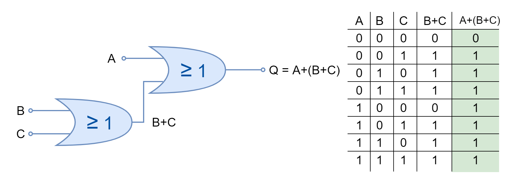
For a three-input logic gate or circuit, a total of eight (8) combinations are possible using above given formula. The combinations of states for two inputs (X, Y & Z) are:
Input Combination 1 = [X=0, Y=0, Z=0]
Input Combination 2 = [X=0, Y=0, Z=1]
Input Combination 3 = [X=0, Y=1 Z=0]
Input Combination 4 = [X=0, Y=1, Z=1]
Input Combination 5 = [X=1, Y=0, Z=0]
Input Combination 6 = [X=1, Y=0, Z=1]
Input Combination 7 = [X=1, Y=1, Z=0]
Input Combination 8 = [X=1, Y=1, Z=1]
Similarly, a four-input logic gate or circuit can have a total of 16 possible combinations. However, in this article, more than a three-input logic gate or circuit is not used for the sake of simplicity. The Truth Tables constructed for two and three inputs represents the logic that can be used to construct Truth Tables for a digital circuit having any number of inputs.
The Truth Tables of logic gates along with their symbols and expressions are given below.
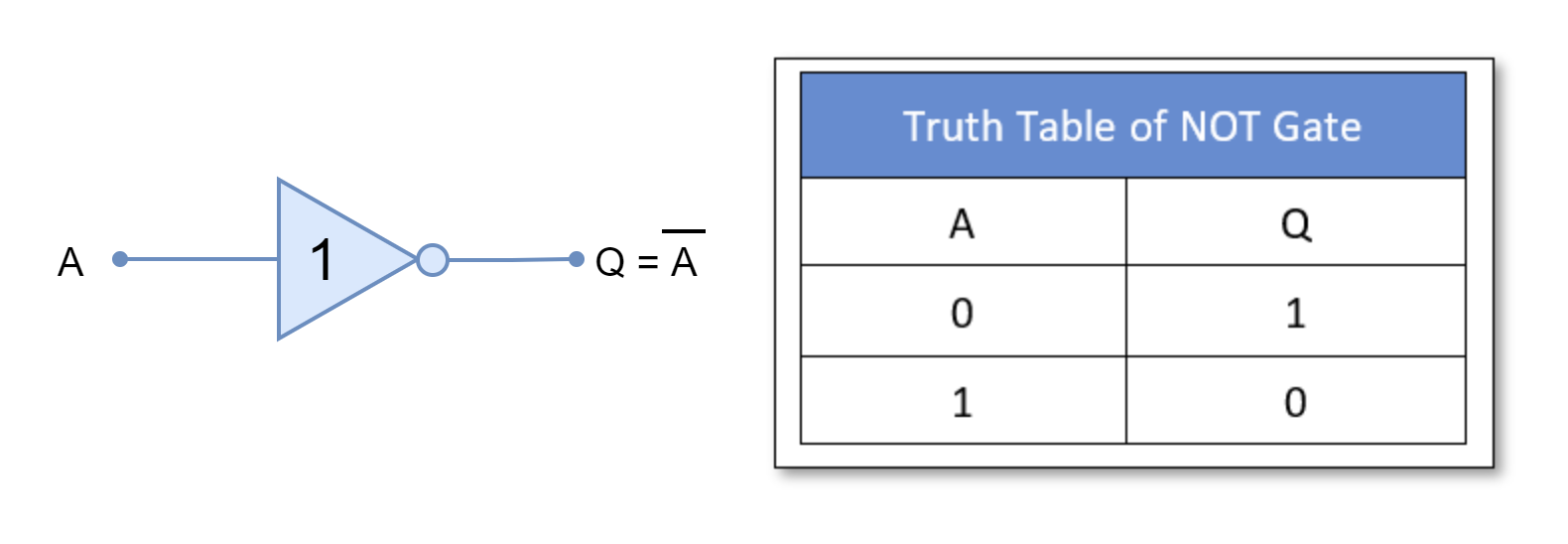
NOT Gate
It is a single input gate and inverts or complements the input. For example, it outputs a “TRUE” or “1” when input is “FALSE” or “0” and vice versa.
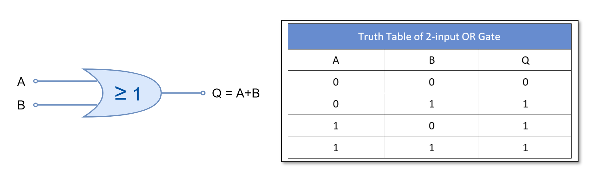
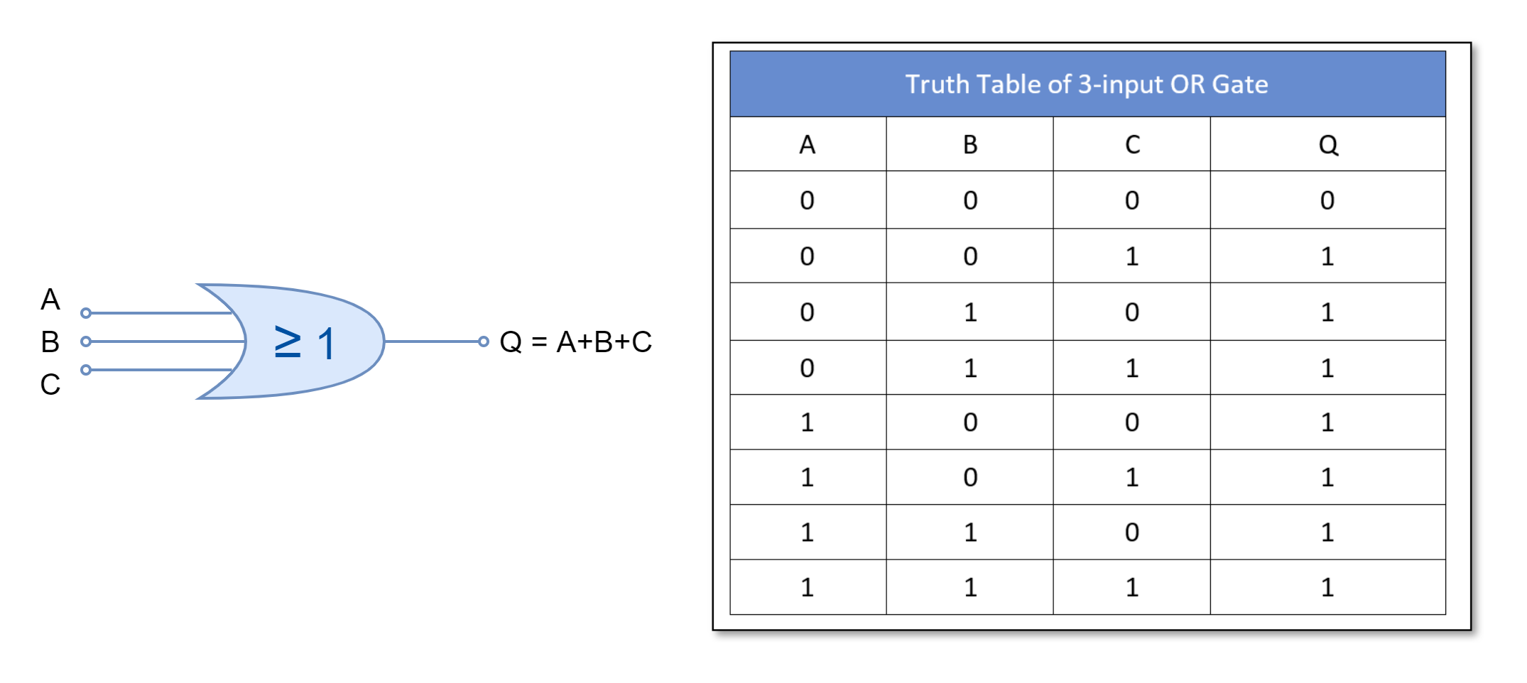
OR Gate
The OR gate outputs “TRUE” or “1” for all input combinations except when all of its inputs are “FALSE” or “0”.
For two-inputs OR gate:
For three-inputs OR gate:
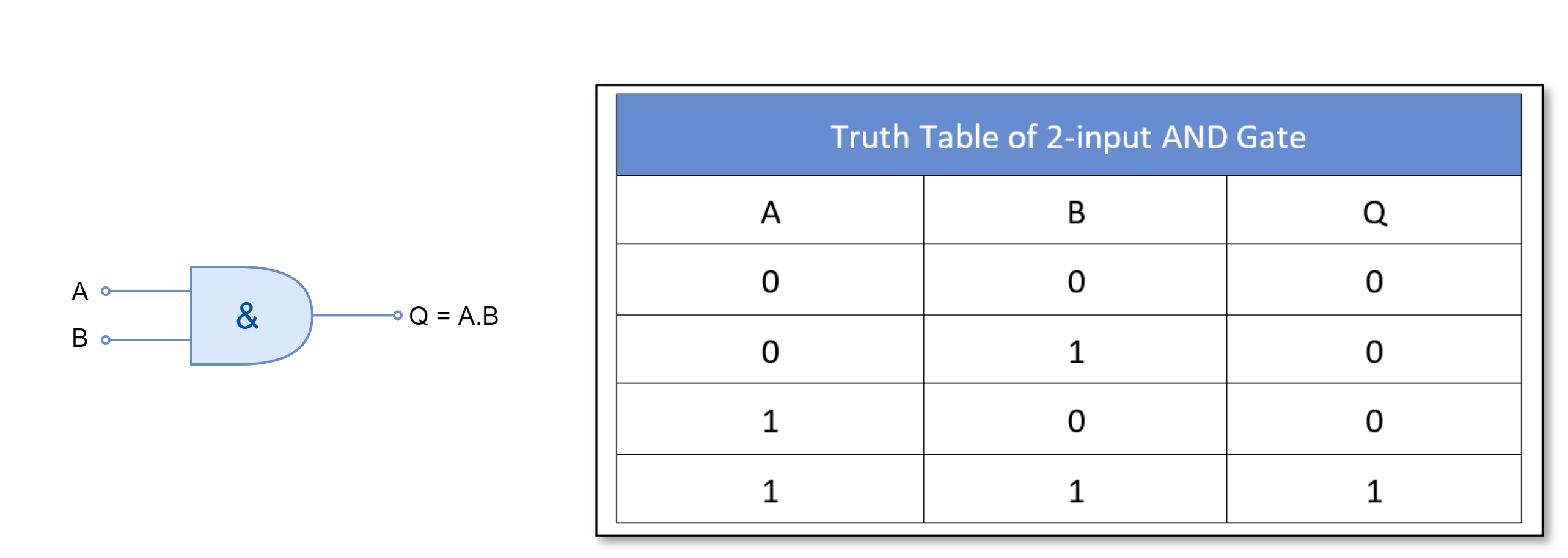
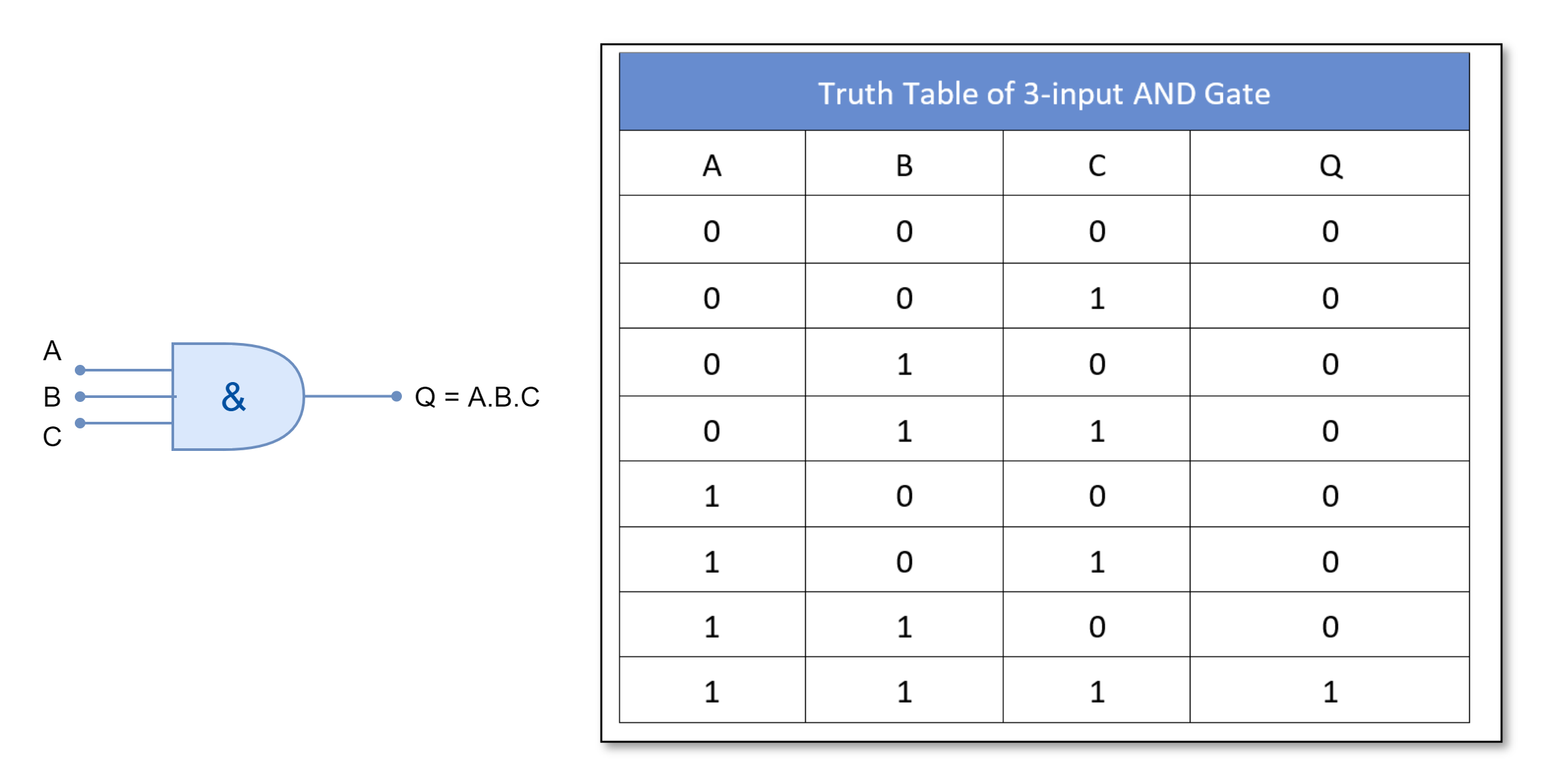
AND Gate
The AND gate outputs “TRUE” or “1” only when all of its inputs are “TRUE” or “1”.
For a two-inputs AND gate:
For a three-input AND gate:
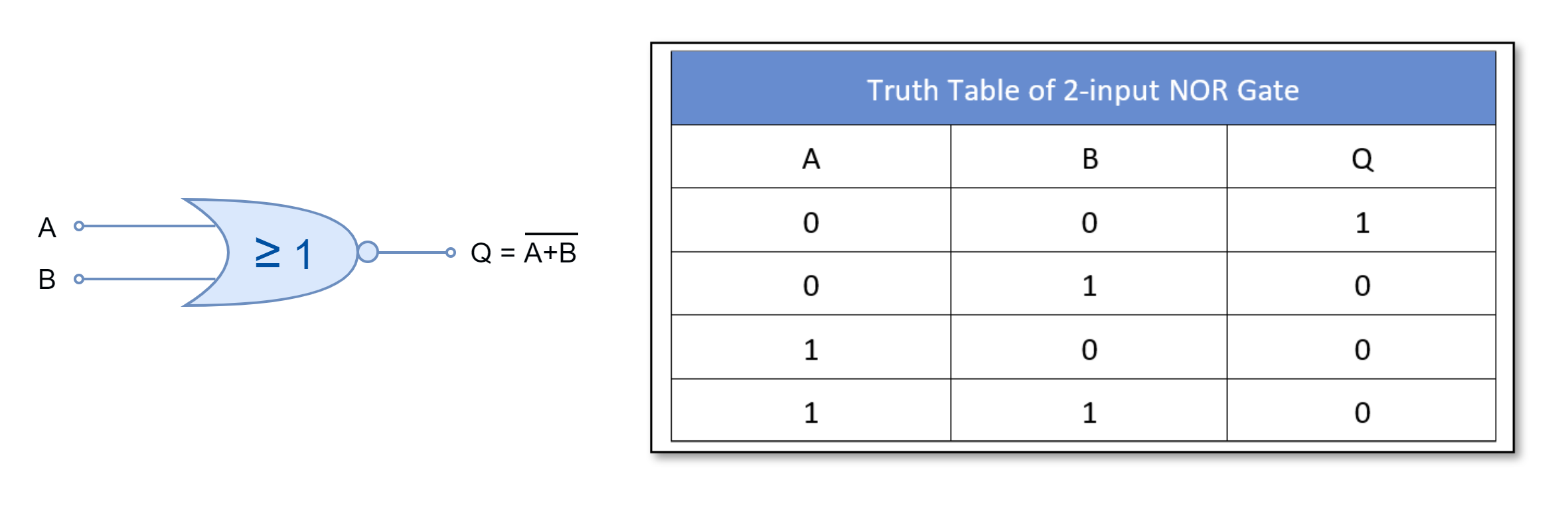
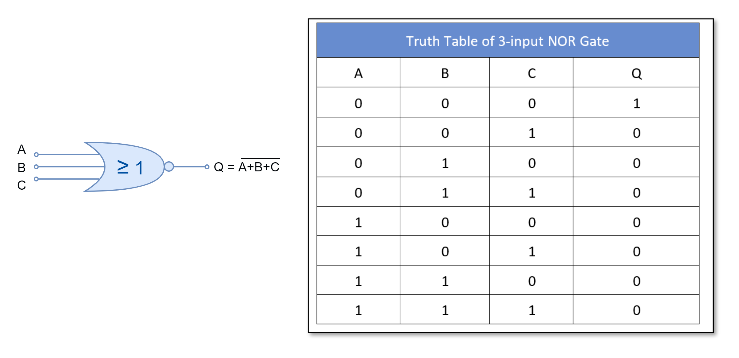
NOR Gate
The NOR gate is the inverted form of OR gate i.e. a NOT gate is placed at the of an OR gate constitute a NOR gate. It outputs “FALSE” or “0” for all input combinations except when all of its inputs are “FALSE” or “0”.
For two-inputs NOR gate:
For three-inputs NOR gate:
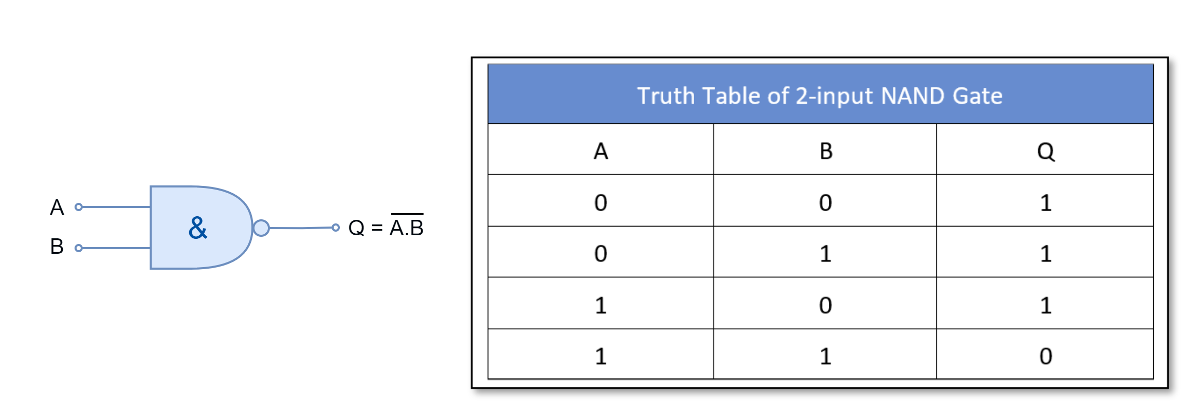
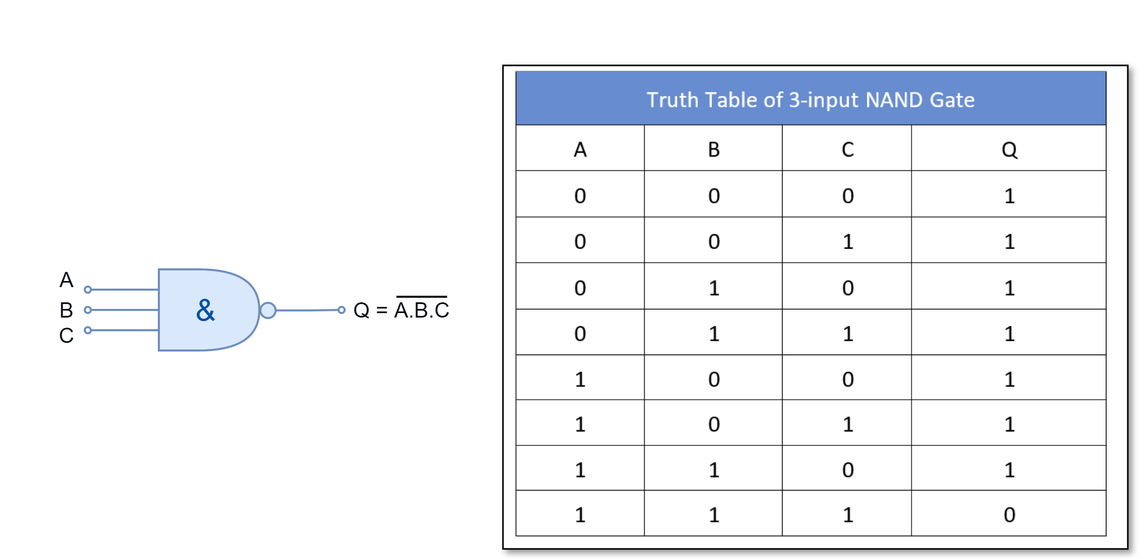
NAND Gate
The NAND gate is the inverted form of AND gate i.e. a NOT gate is placed at the of a AND gate constituting a NAND gate. It outputs “FALSE” or “0” only when all of its inputs are “TRUE” or “1”.
For two-inputs NAND gate:
For three-inputs NAND gate:
Besides, the above-mentioned logic gates, the Exclusive-OR (XOR) and Exclusive-NOR (XNOR) gates represent the most widely and commonly used logic. These logics are used in arithmetic computations and data checking circuits etc. Due to their importance in logic circuits, they are available in digital I.C. packages and hereby included in the article.
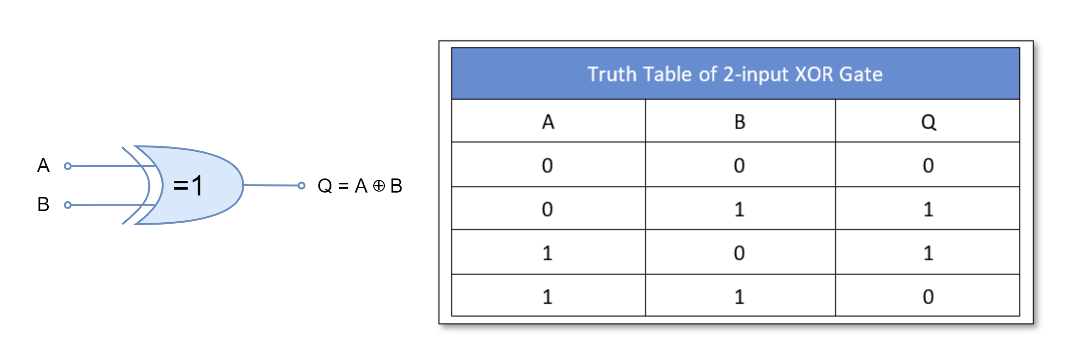
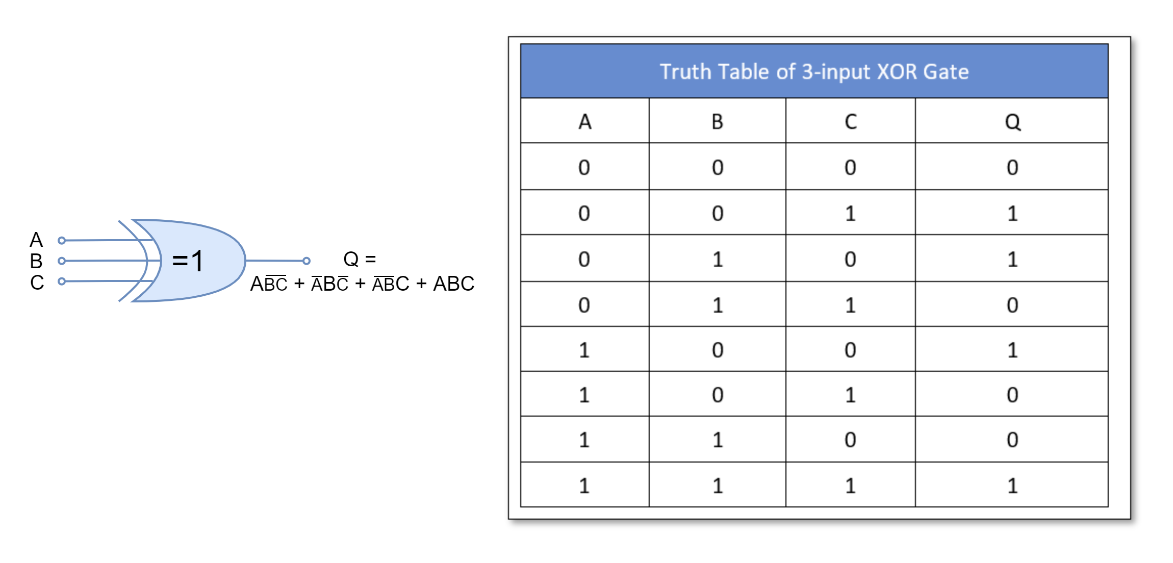
Exclusive-OR (XOR) Gate
The Exclusive-OR (XOR) gate outputs “TRUE” or “1” if either input is in “TRUE” or “1” state. Its output is “FALSE” or “0” when inputs are in the same state.
For two-inputs XOR gate:
For three-inputs XOR gate:
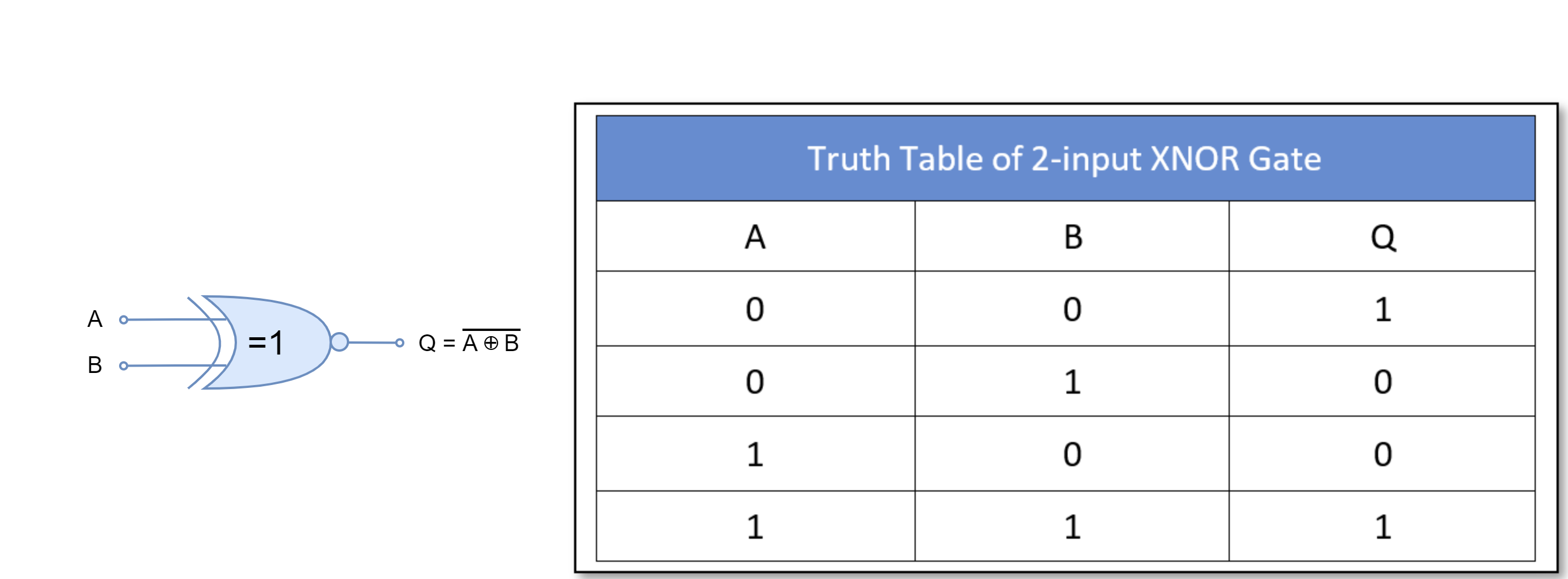
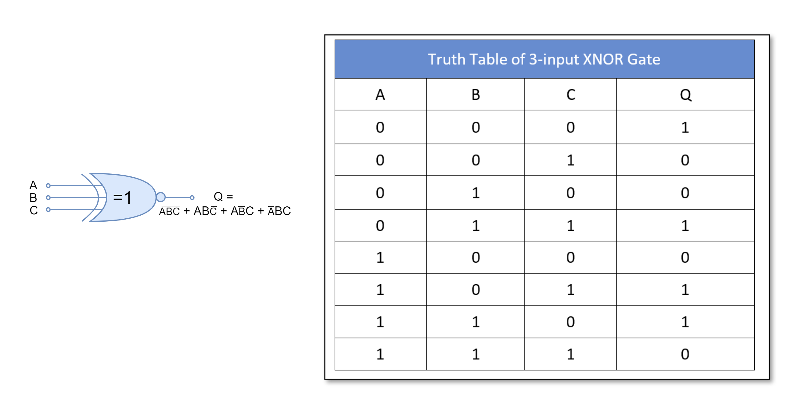
Exclusive-NOR (XOR) Gate
The Exclusive-NOR (XNOR) gate inverts the Exclusive-OR (XOR) gate. Its output is “FLASE” or “0” if either input is in the “TRUE” or “1” state. Its output is “TRUE” or “1” when inputs are in the same state.
For two-inputs XNOR gate:
For three-inputs XNOR gate:
Example of Truth Table
In the following figure, a Truth Table is constructed from the given logic diagram. The Truth Table constructed, shows the output of each logic gate against the input combinations besides the overall function logic circuit output.
Conclusion
- The Truth Table is a tabular form to express the function of a logic gate or logic circuit.
- The Truth Table can express the function of individual logic and overall logic circuit against the combination of input states.
- The total number of inputs states or combinations can be found using 2^n where “n” represents a total number of inputs to the logic gate or circuit.
- The commonly used logic functions are:
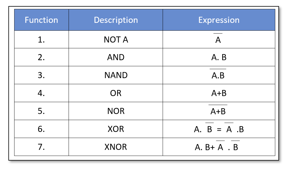
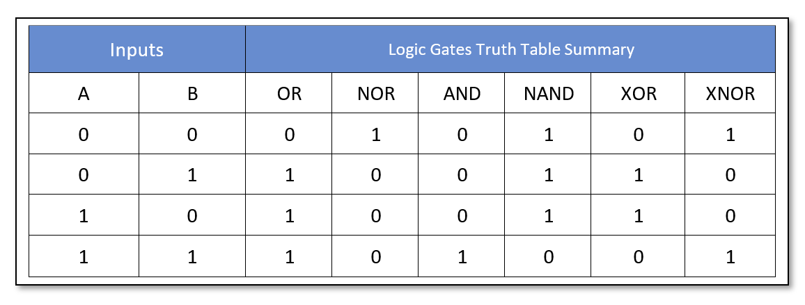
- The Truth Table of commonly used logic gates having two-input is: