AAEON Launches NanoCOM-TGU, a COM Express Type 10 Powered by the 11th Generation Intel® Core™ Processor Family

To optimize embedded and mobile applications for today’s IoT requirements, AAEON, a leading manufacturer of advanced hardware platforms for SDN, NFV, SD-WAN and white box uCPE solutions, today announced the launch of  NanoCOM-TGU, a COM Express Type 10 Powered by the 11th Generation Intel® Core™ Processor Family (formerly Tiger Lake UP3). Our NanoCOM-TGU not only offers powerful computing capability, but also the graphical processing power enabled by Intel® UHD Graphics to optimize AI and Deep Learning applications in COM Express Type 10 mini form factor (84mm x 55 mm).

NanoCOM-TGU is powered by the 11th Generation Intel® Core SoC is designed for applications with intensive data and graphic processing needs. The SoC integrates both powerful CPU and GPU, as well as AI and Deep Learning acceleration engines, to accelerate processing capability in embedded mobile applications, such as telematics, public sectors, and Industrial automation.

The mini form factor of COM Express Type 10 of NanoCOM-TGU shortens the design and deployment processes for system designers or integrators in their embedded mobile projects. In addition, by leveraging the Type 10 form factor, NanoCOM-TGU offers the high-speed I/O interfaces to shorten the system design, including one 2.5 Gigabit Ethernet, two display outputs (eDP x 1 and DDI x 1), one high-definition audio output, two SATA 3.0 interfaces, one onboard PCIe NVMe SSD (up to 256GB), ten USBs (USB 2.0 x 8 and USB 3.2 Gen 2 x 2), two UARTs and PCI-Express [x1] x 4.

To meet the required memory bandwidth and storage performance, NanoCOM-TGU supports LPDDR4x memory with in-band ECC up to 16GB for IoT and Big Data related applications. The onboard PCIe NVMe SSD interface supports up to 256GB and accelerates read/write speeds multiple times than conventional storage interfaces.

System designers or integrators can also be benefited from graphical processing power enabled by Intel® UHD Graphics in NanoCOM-TGU for enhanced visual performance.

more information: www.aaeon.com

Frequency To Voltage Converter (Tachometer) – Variable Reluctance Magnetic Pickup to Voltage Converter

The circuit shown here is a frequency-to-voltage converter that can be used in many applications. This is a signal conditioner for Variable Reluctance Magnetic Pickup Sensor used in engines or machines to detect the speed by sensing gears’ teeth. The input signal level is 20mV to 28V. The circuit provides 1V (67Hz/Volt) when the input frequency is 67Hz with a 15V power supply. The maximum input frequency is 1Khz. The project was built using LM2907N-8 IC, refer to the datasheet of the chip for more information and various configurations. CN1 connector is provided to connect the sensor or input signal. D1 power LED, CN2 Power input, and Voltage output. Use the formula below to calculate voltage output from the desired frequency input.

VOUT = fIN × VCC × R3 × C4

The LM2907 series of tachometer circuits are designed for minimum external part count applications and maximum versatility. To fully exploit its features and advantages, first examine its theory of operation. The first stage of the operation is a differential amplifier driving a positive feedback flip-flop circuit. The input threshold voltage is the amount of differential input voltage at which the output of this stage changes state. Two options (8-pin LM2907 and LM2917) have one input internally grounded so that an input signal must swing above and below ground and exceed the input thresholds to produce an output. This is offered specifically for magnetic variable reluctance pickups which typically provide a single-ended AC output. This single input is also fully protected against voltage swings to ±28 V, which are easily attained with these types of pickups. The differential input options (LM2907, LM2917) give the user the option of setting his input switching level and still having the hysteresis around that level for excellent noise rejection in any application. Of course, to allow the inputs to attain common-mode voltages above ground, input protection is removed and neither input should be taken outside the limits of the supply voltage being used. It is very important that an input not go below ground without some resistance in its lead to limit the current that will then flow in the epi-substrate diode. Following the input stage is the charge pump where the input frequency is converted to a DC voltage. To do this requires one timing capacitor, one output resistor, and an integrating or filter capacitor. When the input stage changes state (due to a suitable zero crossing or differential voltage on the input) the timing capacitor is either charged or discharged linearly between two voltages whose difference is VCC/2. Then in one-half cycle of the input frequency or a time equal to 1/2 fIN the change in charge on the timing capacitor is equal to VCC/2 × C1.

Features

  • Operating Supply 15V DC
  • Output 67Hz/Volt (67Hz = 1Volt)
  • Maximum input Frequency 1Khz
  • Ground Referenced Tachometer Input Interfaces Directly with Variable Reluctance Magnetic Pickups
  • Ground-Referenced Tachometer is Fully Protected from Damage Due to Swings Above VCC and Below Ground
  • Output Swings to Ground for Zero Frequency Input
  • Frequency Doubling for Low Ripple
  • Input Signal Level 20mV to 28V
  • PCB dimensions: 31.12 x 12.86 mm

Applications

  • Variable Reluctance Magnetic Pickup to Voltage Converter
  • Sound Signal to Voltage Converter
  • Speedo Meter
  • Under or Over Speed Sensing
  • Touch Sensor
  • Frequency to Voltage Converter

Schematic

Parts List

NOQNTYREFDESCMANUFACTURERSUPPLIERPART NO
11CN12 PIN MALE HEADER PITCH 2.54MMWURTHDIGIKEY732-5315-ND
21CN24PIN MALE HEADER PITCH 2.54MMWURTHDIGIKEY732-5317-ND
31C110uF/25V SMD SIZE 1206MURATA/YAGEODIGIKEY
41C20.1uF/50V SMD SIZE 0805MURATA/YAGEODIGIKEY
53PR1,R2,C3DNP
61C40.01uF/50V SMD SIZE 1206MURATA/YAGEODIGIKEY
71C51uF/25V SMD SIZE 1206MURATA/YAGEODIGIKEY
81D1LED SMD SIZE 0805LITE ON INCDIGIKEY160-1427-1-ND
91R11K5 5% SMD SIZE 0805MURATA/YAGEODIGIKEY
101R3100K 5% SMD SIZE 0805MURATA/YAGEODIGIKEY
111R410K 5% SMD SIZE 0805MURATA/YAGEODIGIKEY
121U1LM2907N-8TIDIGIKEYLM2907N-8/NOPB-ND

Application Diagram

Connections

Gerber View

Photos

Video

LM2907 Datasheet

Hi-End Microphone Preamplifier with Variable Compression, Noise Gating and Adjustable Gain

The circuit shown here is a complete microphone signal conditioning system based on a single SSM2166 integrated circuit. Designed primarily for voiceband applications, this integrated circuit provides amplification, RMS detection, limiting, variable compression, and downward expansion. An integral voltage-controlled amplifier (VCA) provides up to 60dB of gain in the signal path with approximately 30kHz bandwidth. Additional gain is provided by an input buffer OPAMP circuit that can be set anywhere from 0 dB to 20 dB, for a total signal path gain of up to 80 dB. The project operates on a single +5 V supply, accepts input signals up to 1Vrms, and produces output signal levels > 1 Vrms (3Vp-p) into loads > 5 kΩ. The internal RMS detector has a time constant set by an external capacitor. The SSM2166 contains an input buffer and automatic gain control (AGC) circuit for audio and voiceband signals. Circuit operation is optimized by providing a user-adjustable time constant and compression ratio. A downward expansion (noise gating) feature eliminates circuit noise in the absence of an input signal. Onboard trimmer potentiometer allows the user to set the downward expansion threshold, the limiting threshold (rotation point), input buffer fixed gain, and the internal VCA’s nominal gain at the rotation point.

Features

  • Operating Supply 5V DC (4.5V to 5.5V)
  • Supports Condenser Microphone
  • Adjustable Compressions Ration using Trimmer Potentiometer
  • Adjustable Rotation Point using Trimmer Potentiometer
  • Adjustable Noise Gate Threshold using Trimmer Potentiometer
  • Header Connector for Microphone
  • Header Connector for Output
  • Header Connector for Supply input
  • Low Noise and Distortion
  • Power-Down Feature
  • 20 kHz Bandwidth (61 dB)
  • Power LED D1
  • PCB Dimensions 36.99 x 26.51 mm

Compression Ratio (Can be set Using Optional Fixed Resistor R9 or Trimmer Potentiometer PR4)

The compression ratio may be varied from 1:1 (no compression) to over 15:1 via a Trimmer potentiometer PR4 or Optional resistor R9, RCOMP. Input signals above VRP are compressed with a fixed compression ratio of approximately 15:1. The compression ratio can be set by adjustable trimmer Pot PR4 connected between the COMP RATIO pin (Pin 10) and GND or optional R9. Lowering RCOMP gives smaller compression ratios. with values of about 17 kΩ or less resulting in a compression ratio of 1:1. AGC performance is achieved with compression ratios between 2:1 and 15:1, and is dependent on the application. A 100 kΩ potentiometer PR4 used to allow this parameter to be adjusted.

This region of operation is the “limiting region.” Varying the compression ratio has no effect on the limiting region. The breakpoint between the compression region and the limiting region is referred to as the “limiting threshold” or the “rotation point,” and is user-specified in the SSM2166. The term “rotation point” derives from the observation that the straight line in the compression region “rotates” about this point on the input/output characteristic as the compression ratio is change

Gain Adjust -Trimmer Potentiometer PR3 or Optional Resistor R3

The maximum gain of the project is set by the GAIN ADJUST Trimmer pot PR3. This resistor, with a range between 1 kΩ and 20 kΩ, will cause the nominal VCA gain to vary from 0 dB to approximately 20 dB, respectively. To set the VCA gain to its maximum can also be achieved by leaving the GAIN ADJUST pin in an OPEN condition (no connect).

The gain of the system with an input signal level of VRP is fixed by RGAIN regardless of the compression ratio, and is the “nominal gain” of the system. The nominal gain of the system may be increased by the user via the onboard VCA by up to 20 dB. Additionally, the input buffer of the SSM2166 is configured to provide fixed gains of 0 dB to 20 dB with R2 and R4. The gain of the VCA at the rotation point is set by the value of an optional resistor R3 or trimmer potentiometer PR3 connected between Pin 2 and GND, RGAIN.

Rotation Point Adjustment – Trimmer Potentiometer PR1 or Optional Resistor R6

Rotation Point. An internal dc reference voltage in the control circuitry, used to set the rotation point. By varying a trimmer potentiometer PR1 or optional resistor R6, connected between the positive supply and the ROTATION POINT SET pin (Pin 11), the rotation point may be varied from approximately 20 mV rms to 1 V rms. From the figure, the rotation point is inversely proportional to RROT PT. For example, a 1 kΩ resistor would typically set the rotation point at 1 V rms, whereas a 55 kΩ resistor would typically set the rotation point at approximately 30 mV rms. Since limiting occurs for signals larger than the rotation point (VIN > VRP), the rotation point effectively sets the maximum output signal level. It is recommended that the rotation point be set at the upper extreme of the range of typical input signals so that the compression region will cover the entire desired input signal range. Occasional larger signal transients will then be attenuated by the action of the limiter.

Noise Gate Adjust – Trimmer Potentiometer PR2 or Optional Resistor R7

The range of the noise gate is from 0.3 mV to over 0.5 mV relative to the output of the buffer. To fit this range to your application, you may have to attenuate the input or apportion the buffer gain and VCA gain differently.

Operations

The audio input signal is processed by the input buffer and then by the VCA. The input buffer presents an input impedance of approximately 180 kΩ to the source. A dc voltage of approximately 1.5 V is present at AUDIO +IN (Pin 7 of the SSM2166), C4 provided as a blocking capacitor for ground-referenced sources. A 0.1 µF capacitor is a good choice for most audio applications. The input buffer is a unity-gain stable amplifier that can drive the low impedance input of the VCA. The VCA is a low distortion, variable-gain amplifier whose gain is set by the side-chain control circuitry. The input to the VCA is a virtual ground in series with approximately 1 kΩ. Capacitor C3 provided for blocking purpose between the buffer’s output and the VCA input. The 1 kΩ impedance between amplifiers determines the value of this capacitor which is typically between 10 µF. The VCA amplifies the input signal current flowing through C3 and converts this current to a voltage at the SSM2166’s output pin (Pin 13). The net gain from input to output can be as high as 60 dB (without additional buffer gain), depending on the gain set by the control circuitry.

The gain of the VCA at the rotation point is set by the value of a resistor connected between Pin 2 and GND, RGAIN. The AGC range of the SSM2166 can be as high as 60 dB. The VCAIN pin (Pin 3) on the SSM2166 is the noninverting input terminal to the VCA. The output impedance of the SSM2166 is typically less than 75 Ω, and the external load on Pin 13 should be >5 kΩ. The nominal output dc voltage of the device is approximately 2.2 V. Capacitor C8 provided on output for blocking purpose for grounded loads. The bandwidth of the SSM2166 is quite wide at all gain settings. The upper 3 dB point is approximately 30 kHz at gains as high as 60 dB (using the input buffer for additional gain, circuit bandwidth is unaffected). The lower 3 dB cut-off frequency of the SSM2166 is set by the input impedance of the VCA (1 kΩ) and C3. While the noise of the input buffer is fixed, the input referred noise of the VCA is a function of gain. The VCA input noise is designed to be a minimum when the gain is at a maximum.

The Level Detector

The SSM2166 incorporates a full-wave rectifier and a patent-pending, true RMS level detector circuit whose averaging time constant is set by an external capacitor C6 connected to the AVG CAP pin (Pin 8). For optimal low frequency operation of the level detector down to 10 Hz, the value of the capacitor should be 2.2 µF. Some experimentation with larger values for the AVG CAP may be necessary to reduce the effects of excessive low frequency ambient background noise. The value of the averaging capacitor affects sound quality: too small a value for this capacitor may cause a “pumping effect” for some signals, while too large a value can result in slow response times to signal dynamics. Electrolytic capacitors are recommended here for lowest cost and should be in the range of 2 µF to 47 µF. Capacitor values from 18 µF to 22 µF have been found to be more appropriate in voiceband applications, where capacitors on the low end of the range seem more appropriate for music program material.

Schematic

Parts List

NOQNTYREFDESCMANUFACTURERSUPPLIERPART NO
11CN1, CN2, CN32 PIN MALE HEADER PITCH 2.54MMWURTHDIGIKEY732-5315-ND
22C1,C40.1uF/50VMURATA/YAGEODIGIKEY
33C2,C3,C510uF/16VMURATA/YAGEODIGIKEY
41C622uF/16VMURATA/YAGEODIGIKEY
51C71uF/16VMURATA/YAGEODIGIKEY
61C81uF/16VMURATA/YAGEODIGIKEY
71D1LED SMD SIZE 0805OSRAMDIGIKEY475-1278-1-ND
81PR4100K TRIMMER POTBOURNSDIGIKEY3362P-104LF-ND
91PR21M TRIMMER POTBOURNSDIGIKEY3362P-105LF-ND
101PR320K TRIMMER POTBOURNSDIGIKEY3362P-203LF-ND
113R1,R2,R410KMURATA/YAGEODIGIKEY
122R3,R51KMURATA/YAGEODIGIKEY
134R6,R7,R8,R9DNP
141U1SSM2166ANALOGDIGIKEY2156-SSM2166S-AD-ND
151PR150K TRIMMER POTBOURNSDIGIKEY3362P-503LF-ND

Connections

Gerber View

Photos

Video

SSM2166 Datasheet

250V AC Isolated Voltage-Sensing Circuit with Single output (250V AC Input 5V Output)

The project presented here can be used in isolated voltage sensing measurements applications. The board was built using ISO224B isolated amplifier, isolated 5V DC-DC converter provides 5V DC to the input side of ISO224 amplifier, TLV6001 op-circuit converts the differential signal of ISO224 and provides single-ended output. The circuit measures the 250V AC voltage and outputs a 5V signal, the output is optically isolated and the output voltage will change proportional to the input voltage. The operating supply of the project is a single 5V DC. The divider resistor reduces the voltage from AC 250V to +/-7.5V which is within the input range of ISO224 (+/-12V). The circuit can be used to measure the DC voltage as well AC voltage.

Features

  • Operating Supply 5V DC
  • Onboard Isolated 5V to 5V DC-DC Converter to Power The input Side of ISO224 Amplifier
  • Input 250V AC
  • Frequency Response 1Hz to 20Khz (Tested)
  • Can be Configured to Measure the DC +/-7.5V DC or Higher
  • Can be Configured for differential Output
  • Output 5V
  • Onboard Power LED
  • PCB Dimensions 53.50 x 25.24 mm

AC Voltage Measurement

The existing circuit can measure the AC voltage up to 250V AC and provide a 5V sinewave, output level depends on the input voltage level. When the input is off, the output is 2.5V DC. Users may change the input to output ratio by altering input divider resistors R3, R4, R5, R6, and R8. It is recommended to use 1% tolerance for all these resistors, C4 is to prevent the noise coming from input. This board can be configured to measure the +/-480V by altering the values of the divider resistors.

DC Voltage Measurement

This circuit can measure dual input +/-7.5V DC and provides 0 to 5V DC (2.5V DC when input is Zero or OFF). When R3, R4, R5, R6, resistor values are 0 Ohms and R8 is not used. For higher voltage measurement use appropriate divider resistors R3, R4, R5, R6, R8. It is important to maintain a maximum output of +/-7.5V after divider resistors.

Differential Output for ADC Interface

Make the following changes to configure this board for differential output

  • Do not Install R1, R2, R10, R7, R9, R12, C6, C5, U3, CN2
  • Use CN3 for the interface: Pin 1 VCC-5V DC input, Pin 2 +P Output for ADC, Pin 3 -N Output for ADC, Pin 4 GND
  • R3, R4, R5, R6 = 0 Ohms 1206 size, do not install R8
  • Project Provides differential output +/-4V with input +/-12V
  • Calculate and Choose divider resistor R3, R4, R5, R6, and R8 for higher voltage measurements

This board can be configured for differential output which is important for analog-to-digital converters (ADC) interface. ISO224 is optimized for accurate sensing of +/-12V signals that are widely used in industrial applications. Do not populate the following components R1, R2, R10, R7, R9, R12, C6, C5, U3, CN2 to optimize the board for differential output. Optional Connector CN3 helps for the ADC interface.

The ISO224 is a precision isolated amplifier with an output separated from the input circuitry by an isolation barrier with high immunity to magnetic interference. This barrier is certified to provide reinforced galvanic isolation of up to 5 kVRMS with an exceptionally long lifetime and low power dissipation. When used with isolated power supplies, this device separates parts of the system that operate on different common-mode voltage levels and protects lower-voltage devices from damage. The input of the ISO224 is optimized for accurate sensing of ±10-V signals that are widely used in industrial applications. The device operates of a single supply on the high side. This unique feature simplifies the design of the isolated power supply and reduces the system cost. The integrated high-side supply voltage detection feature simplifies system-level diagnostics. The ±4-V output of the ISO224 allows lower-cost analog-to-digital converters (ADCs) to be used. The differential structure of the output supports high immunity to noise.

Schematic

Parts List

NO.QNTY.REF.DESC.MANUFACTURERSUPPLIERPART NO
11CN12 PIN SCREW TERMINAL PITCH 5.08MMPHOENIXDIGIKEY277-1247-ND
21CN24 PIN MALE HEADER PITCH 2.54MMWURTHDIGIKEY732-5317-ND
31CN3DNP
42C1,C1210uF/16V SMD SIZE 1206MURATA/YAGEODIGIKEY
54C2,C7,C9,C110.1uF/50V SMD SIZE 0805MURATA/YAGEODIGIKEY
61C30.22uF/50V SMD SIZE 0805MURATA/YAGEODIGIKEY
72C4,C5100PF/50V SMD SIZE 0805MURATA/YAGEODIGIKEY
81C633PF/50V SMD SIZE 0805MURATA/YAGEODIGIKEY
92C8,C1010uF/16V SMD SIZE 1210MURATA/YAGEODIGIKEY
102D1,D2PD3S120L-7DIODE INCORPDIGIKEYPD3S120LQ-7DICT-ND
111D3LED SMD SIZE 0805OSRAMDIGIKEY475-1278-1-ND
122R1,R2220K 1% SMD SIZE 0805MURATA/YAGEODIGIKEY
133R3,R4,R5150K 1% SMD SIZE 1206MURATA/YAGEODIGIKEY
141R61E 5% SMD SIZE 1206MURATA/YAGEODIGIKEY
153R7,R9,R12105K 1% SMD SIZE 0805MURATA/YAGEODIGIKEY
161R810K % SMD SIZE 1206MURATA/YAGEODIGIKEY
171R1047E 5% SMD SIZE 0805MURATA/YAGEODIGIKEY
181R111K 5% SMD SIZE 0805MURATA/YAGEODIGIKEY
191TR1750313769 TRANSFORMERWURTHDIGIKEY1297-1107-1-ND
201U1ISO224BTIDIGIKEY296-52316-1-ND
211U2LM1117-5VTIDIGIKEYLM1117MPX-5.0CT-ND
221U3TLV6001IDBVRTIDIGIKEY296-TLV6001IDBVRCT-ND
231U4SN6501TIDIGIKEY296-30388-1-ND

Block Diagram

Connections

Input vs Output

Gerber View

Photos


Video


ISO224 Datasheet

Carrier Board for Advanced Phase-Shift PWM Controller UCC3895

This is a Phase-Shifted Full-Bridge PWM UCC3895 carrier board that contains all of the features necessary to implement a phase-shifted full-bridge topology power converter. All inputs and outputs pins are accessible using a header connector. A highly-efficient DC-DC converter can be created using this carrier board + External H-Bridge and Transformer. Refer to the datasheet of UC3895 and schematic to configure the working frequency, current feedback, delays, etc.

The UCC3895 is a phase-shift PWM controller that implements control of a full-bridge power stage by phase-shifting the switching of one half-bridge with respect to the other. The device allows constant frequency pulse-width modulation in conjunction with resonant zero-voltage switching to provide high efficiency at high frequencies. The part is used either as a voltage-mode or current-mode controller. While the UCC3895 maintains the functionality of the UC3875/6/7/8 family and UC3879, it improves on that controller family with additional features such as enhanced control logic, adaptive delay set, and shutdown capability. Because the device is built using the BCDMOS process, it operates with dramatically less supply current than its bipolar counterparts. The UCC3895 operates with a maximum clock frequency of 1 MHz.

Note: This is a carrier board for UCC3895 phase-shift chip, refer to the datasheet of UCC3895 IC to learn more about setting up the delay, current sense, duty cycle, frequency.

Features

  • Operating Power-Supply 10V to 16.5V DC
  • Default Frequency 195Khz
  • Programmable-output turn-on delay
  • Adaptive delay set
  • Bidirectional oscillator synchronization
  • Voltage-mode, peak current-mode, or average
  • current-mode control
  • Programmable soft start, soft stop, and chip
  • disable via a single pin
  • 0% to 100% duty-cycle control
  • 7-MHz error amplifier
  • Operation up to 1 MHz
  • Typical 5-mA operating current at 500 kHz
  • Very low 150-μA current during UVLO
  • PCB dimensions: 24.40 x 26.04 mm

Connector CN1 Pinout

  • Pin 1 VDD 10V to 16.5V DC
  • Pin 2 VREF Output 5V DC
  • Pin 3 Error Amplifier (EA)
  • Pin 4 Output A
  • Pin 5 Output B
  • Pin 6 Output C
  • Pin 7 Output D
  • Pin 8 Current Sense In
  • Pin 9 GND
  • Pin 10 Not Connected ( NC)

Schematic

Application Diagram

Parts List

NO.QNTY.REF.DESC.MANUFACTURERSUPPLIERPART NO
11CN110 PIN MALE HEADER RIGHT ANGLE PITCH 2.54MMWURTHDIGIKEY732-2670-ND
21C10.022uF/50V SMD SIZE 0805MURATA/YAGEODIGIKEY
32C2,C81KPF/50V SIZE 0805MURATA/YAGEODIGIKEY
41C31uF/50V SMD SIZE 0805MURATA/YAGEODIGIKEY
51C456PF/50V SMD SIZE 0805MURATA/YAGEODIGIKEY
61C510uF/25V SMD SIZE 1206MURATA/YAGEODIGIKEY
71C6330PF/50V SMD SIZE 0805MURATA/YAGEODIGIKEY
81C70.1uF/50V SMD SIZE 0805MURATA/YAGEODIGIKEY
91D11N4148MICROCHIP TECHMOUSER494-1N4148UR-1
101PR150K TRIMMER POTBOURNSMOUSER3362H-503LF-ND
111Q1BC847ALNEXPERIADIGIKEYBC847B-TPCT-ND
121R18.8K 1% SMD SIZE 0805MURATA/YAGEODIGIKEY
131R2510E 1% SMD SIZE 0805MURATA/YAGEODIGIKEY
141R310K 1% SMD SIZE 0805MURATA/YAGEODIGIKEY
151R421K 1% SMD SIZE 0805MURATA/YAGEODIGIKEY
161R52K 1% SMD SIZE 0805MURATA/YAGEODIGIKEY
171R668K 1% SMD SIZE 0805MURATA/YAGEODIGIKEY
181R7560E 1% SMD SIZE 0805MURATA/YAGEODIGIKEY
191R82.4K 1% SMD SIZE 0805MURATA/YAGEODIGIKEY
202R9,R1010E 5% SMD SIZE 0805MURATA/YAGEODIGIKEY
211R11DNP
221U1UCC3895TIDIGIKEY296-2552-5-ND

Connections

Gerber View

UCC3895 Pin Functions

Photos

Video

UCC3895 Datasheet

49W BTL 4 Channel Audio Power Amplifier

This is a 49W – 4 Channel audio amplifier project that is built using TB2941HQ power Integrated Circuit which has a built-in four-channel BTL amplifier developed for car audio applications. The maximum output power is 49W using a pure complementary P-Ch and N-Ch DMOS output stage. In addition, a standby switch, a mute function, and various protection features are included. The audio mute function is enabled when jumper J1 is connected to 5V DC. The power supply can be turned ON or OFF via pin 4 (Stby). The threshold voltage of pin 4 is 2.2V to VCC (5V). The amplifier is turned ON when standby pin is connected to 5V DC using Jumper CN10. Onboard 5V regulator provided for standby and Mute function. When the headroom voltage is suppressed by the low VCC, the TB2941HQ switches outputs voltage from VCC/2 to VCC/4 and reduces the audible pop noise and the sound cutting. The TB2941HQ can reduce the distortion which is generated by low VCC because this amplifier circuit keeps the voltage gain of BLT outputs. In other words, if one side output of BTL has the voltage margin, its output can make up for the clipped waveform of the other side output.

It is recommended to use appropriate heatsink on IC to prevent overheating.

Features

  • Operating Power Supply 7.5V to 15V DC (VCC 15V = 49W output, VCC 13.7V=40W) THD 10%
  • 49W Output with 4 Ohms Speaker
  • 4XScrew Terminal Connector for Speaker Connections
  • Screw Terminal Connector for Power Supply Input
  • Female RCA Connector for Audio Inputs
  • Voltage Gain GV 26dB
  • Power LED
  • High output power, low distortion, and low noise property
  • Jumper for Mute Function
  • Jumper for Standby Function
  • Thermal Shutdown (Built in IC)
  • Built-in various protection circuits over-voltage, short to VCC, short to GND, and output to output short)
  • PCB Dimensions 79.06 x 51.44 mm

TB2941HQ Features

Thermal Shut Down

  • Thermal shut down operates when the junction temperature exceeds 150°C (typ.).

Auto Muting Functions

  • The TB2941HQ has two automatic mute functions.
  • Low VCC Mute
  • Stand-by Off Mute

Low VCC Mute

  • When the supply voltage became lower than 5.5V (Typ.), The TB2941HQ operates the mute circuit automatically. This function prevents the large audible transient noise which is generated by low VCC

Over-Voltage

  • Over-voltage It operates when the voltage exceeding the operating range is supplied to VCC pin. If the voltage falls, it will return automatically. When it operates, all outputs bias and high-side switch are turned off and all outputs are intercepted. The threshold voltage is 23 V (Typ.)

Standby-Off Mute

  • The TB2941HQ operates the mute circuit during the standby-off transition. When the ripple voltage reached VCC/5, the standby-off mute is terminated. The external mute has to be ON till the internal mute-OFF

Short to VCC

  • Short to VCC, Short to GND, Output to output short It operates when each output pin is in irregular connection and the load line goes over the SOA of the power transistor (DMOS). When it operates, all outputs bias circuits are turned off and all outputs are intercepted. If the irregular connection is canceled, it will return automatically.

Schematic


Parts List

NOQNTY.REFDESC.MANUFACTURERSUPPLIERPART NO
11CN12 PIN SCREW TERMINAL PITCH 5.08MMPHOENIXDIGIKEY277-1247-ND
21CN22 PIN SCREW TERMINAL PITCH 5.08MMPHOENIXDIGIKEY277-1247-ND
31CN32 PIN SCREW TERMINAL PITCH 5.08MMPHOENIXDIGIKEY277-1247-ND
41CN4RCA FEMALECUI DEVICEDIGIKEYCP-1405-ND
51CN5RCA FEMALECUI DEVICEDIGIKEYCP-1405-ND
61CN6RCA FEMALECUI DEVICEDIGIKEYCP-1405-ND
71CN7RCA FEMALECUI DEVICEDIGIKEYCP-1405-ND
81CN82 PIN SCREW TERMINAL PITCH 5.08MMPHOENIXDIGIKEY277-1247-ND
91CN92 PIN SCREW TERMINAL PITCH 5.08MMPHOENIXDIGIKEY277-1247-ND
101CN103 PIN MALE HEADER PITCH 2.54MMWURTHDIGIKEY732-5316-ND
111C13900uF/25VUNITEC CHEMI-CONDIGIKEY565-3901-ND
121C20.1uF/63VEPCOSDIGIKEY495-B32529C1104M289TB-ND
131C31uF/35V SMD SIZE 1206MURATA/YAGEODIGIKEY
144C4,C5,C6,C70.22uF/35V SMD SIZE 1206MURATA/YAGEODIGIKEY
151C810uF/25V ELECTROLYTICRUBYCONDIGIKEY1189-1300-ND
161C90.1uF/50V SMD SIZE 0805MURATA/YAGEODIGIKEY
172C10,C111uF/25VMURATA/YAGEODIGIKEY
181D1LED SMD SIZE 0805LITE ON INCDIGIKEY160-1427-1-ND
191J13 PIN MALE HEADER PITCH 2.54MMWURTHDIGIKEY732-5316-ND
201R10E SMD SIZE 0805MURATA/YAGEODIGIKEY
211R21K 5% SMD SIZE 0805MURATA/YAGEODIGIKEY
222R3,R447K 5% SMD SIZE 0805MURATA/YAGEODIGIKEY
231U1TB2941TOSHIBADIGIKEYTB2941HQ-ND
241U2LM7805C/TOTIDIGIKEY296-47192-ND
252JMPRSHUNT FOR JUMPPERSULINS DIGIKEYS9001-ND

Connections

Gerber View

Photos

Video

TB2941HQ Datasheet

Smartpixels.app Lighting Control Project used to control Christmas lights

story by Tomasz Siroń

I would like to present a project developed with a passion for almost 10 years. It is a non-commercial installation of lights controlled via the Internet. The user can control the illumination in real-time using the panel on the website.

I installed computer-controlled lights for the first time in 2012. I figured if a machine could control lights then why couldn’t a human. The system is in operation for the ninth season. I improve it every year. Krzysztof Styc from Oświęcim (Poland) made a significant contribution to the construction of the website.

He has been involved in the project since 2014. – In the beginning, I was only supposed to help with the site, but I had the idea to share my Christmas tree. After a few problems with powering the lamps, we managed to start the control on the Internet – says Krzysztof Styc (22 years old)

Mateusz Kołoś (19), Wiktor Jezioro (20), Przemysław Kasza (26), Hubert Ryfiński (27) and Marlena Martyna (25) are also involved in the lighting project.

Mateusz and Wiktor deal with the lighting of their properties, provide infrastructure and co-create the website. Przemysław, on the other hand, was the administrator and architect of IT systems adapted to cloud solutions. Marlena supports the team on non-technical issues. She watches over the progress of work in the project (Scrum methodology). She supports the Team in substantive and linguistic matters, being an objective – and sometimes critical – adviser. Hubert deals with issues related to audio-video transmission, e.g. a Christmas nativity scene in Modliborzyce, as well as technical service.

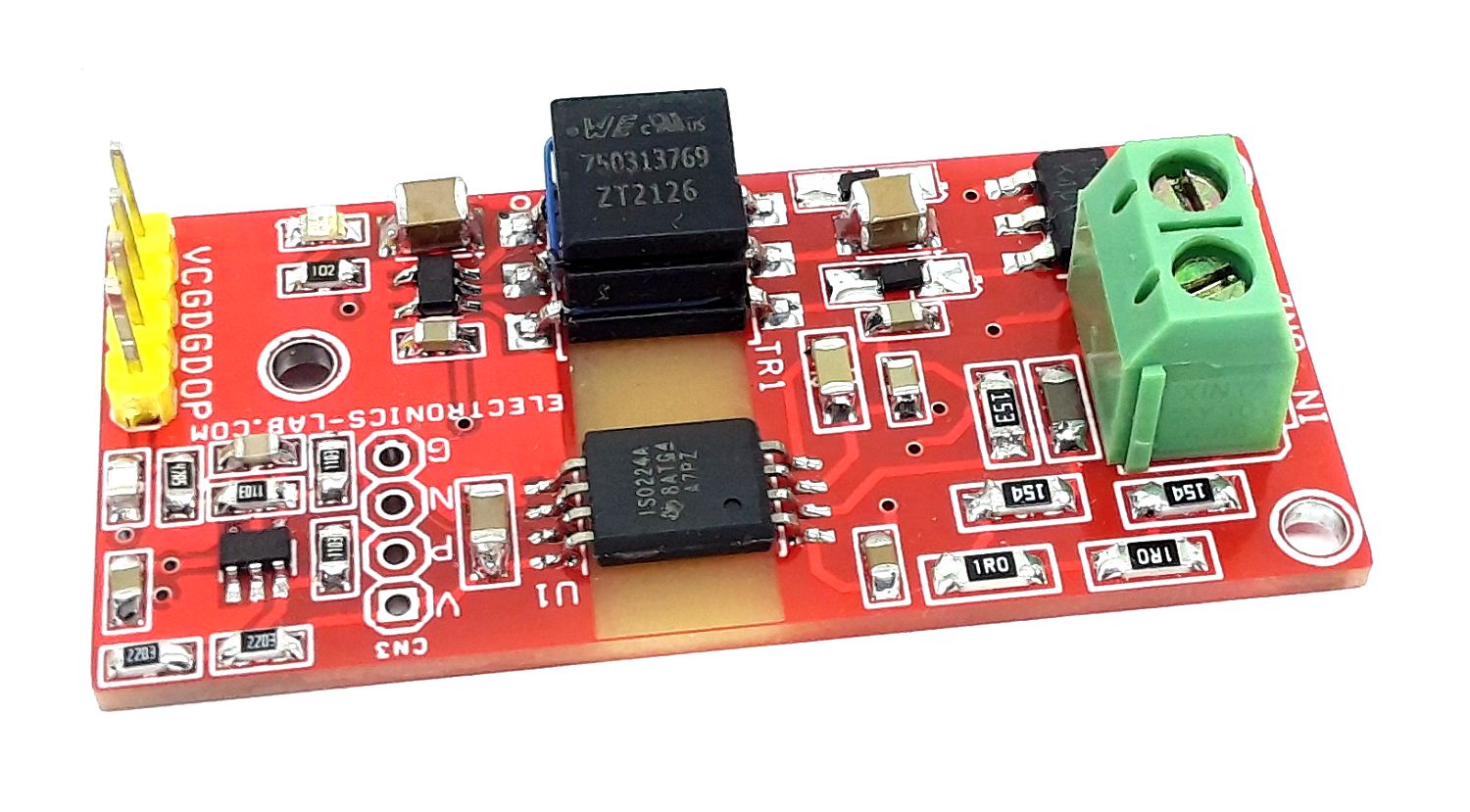
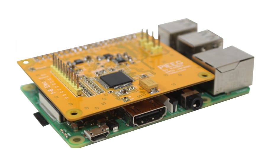
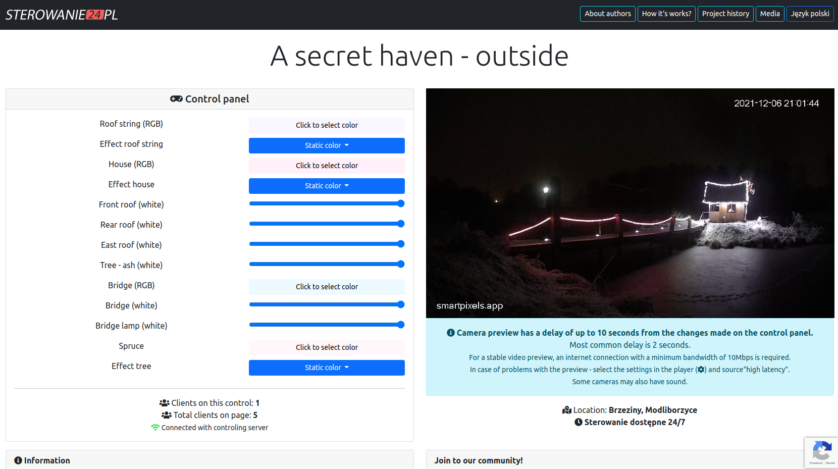
How does the installation work? The lights are connected to controllers (usually ESP8266 or Arduino) linked to the computer (Raspberry Pi). This, in turn, is connected with internet users around the world via smartpixels.app website.

Colors or effects are sent to the controller in a given location via Socket.io software. Each of us has different proprietary controllers, but the whole thing is based on the client’s code written in the Node.js programming language. For lighting, we use: cards with relays, PWM brightness controllers, programmable pixel diodes, LED strips. WLED or ESP Easy software is installed on the microcontroller, which is connected to the drivers of lights.

The web application uses the Node.js programming language – it generates a website with a control panel. Variable page elements are stored in the MySQL database which is replicated between servers. The application is based on the potential of Docker containers, it is run for production in a Kubernetes cluster. To ensure fast implementation of the code, we use the CI/CD (continuous integration and continuous deployment) with GitHub and Docker Hub services.

The user page is delivered from the nearest server through Cloudflare. Production machines communicate with each other via WireGuard VPN working in a mesh configuration. Infrastructure is designed for high availability and the ability to scale quickly.

We have our own video streaming solutions. We use WebRTC and HTTP Live Streaming technologies to deliver camera footage to users. Pictures from cameras are delivered to the server with graphics cards. On the server, images are processed into different quality streams. OvenMediaEngine software allows us to deliver the live view with the lowest possible delay (usually 2 seconds).

As cameras, we usually use consumer surveillance IP cameras, which are calibrated to ensure the highest possible image quality.

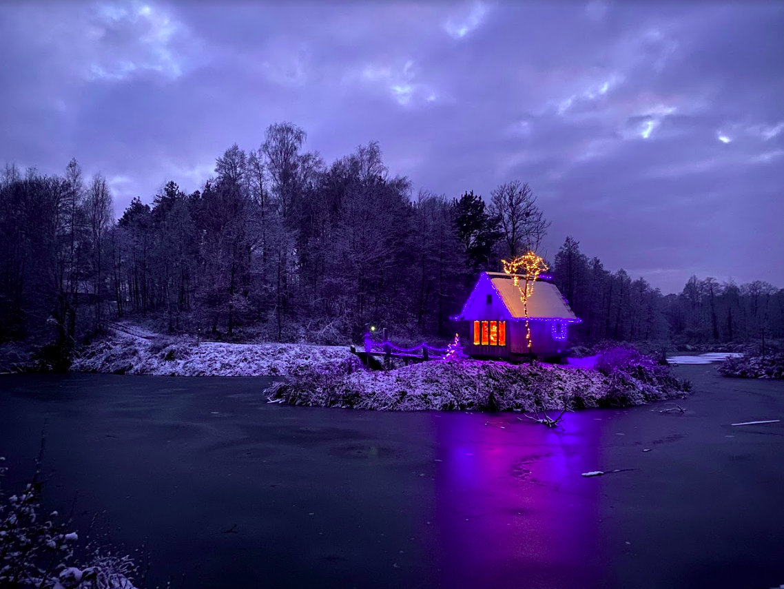
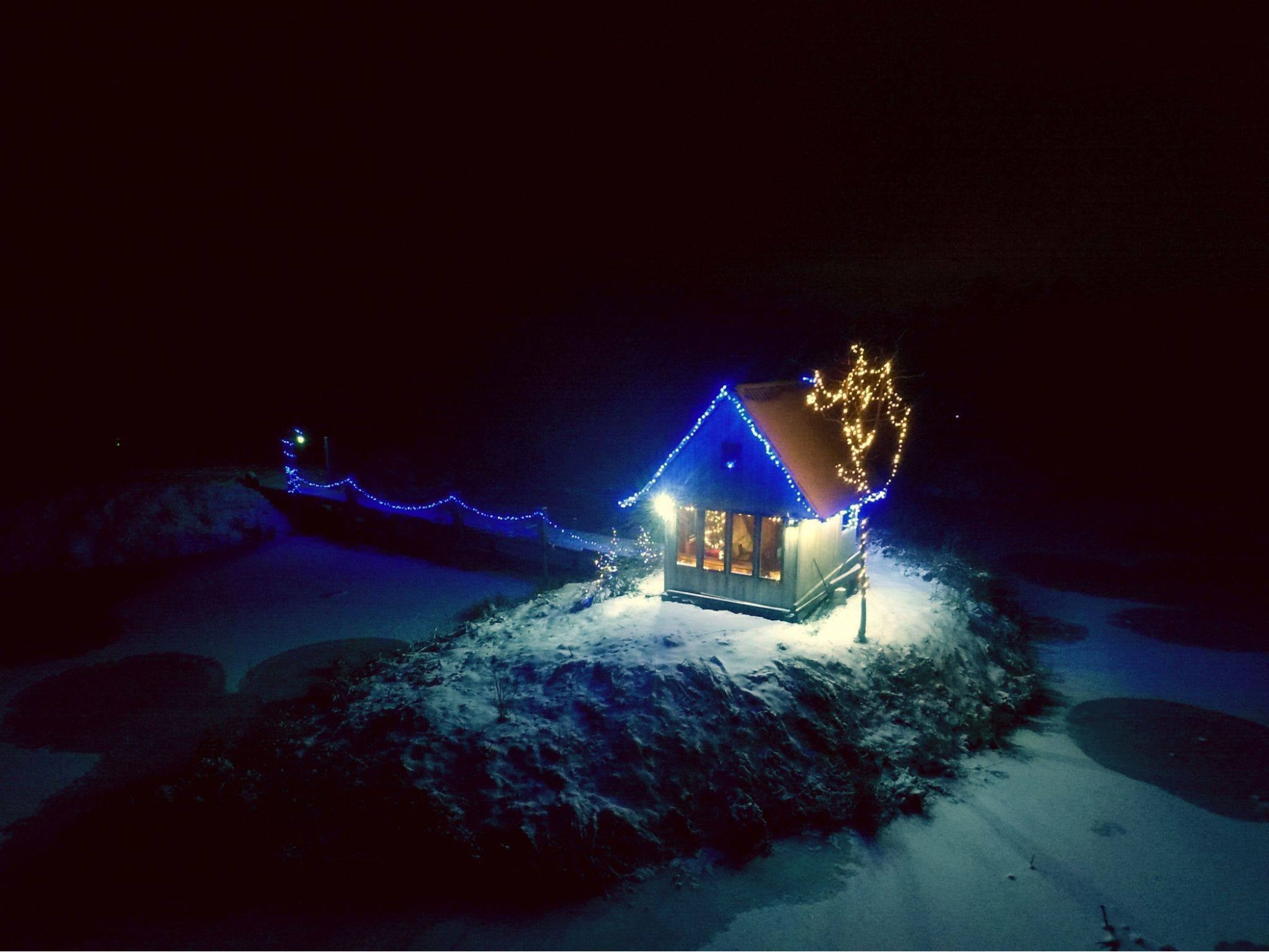
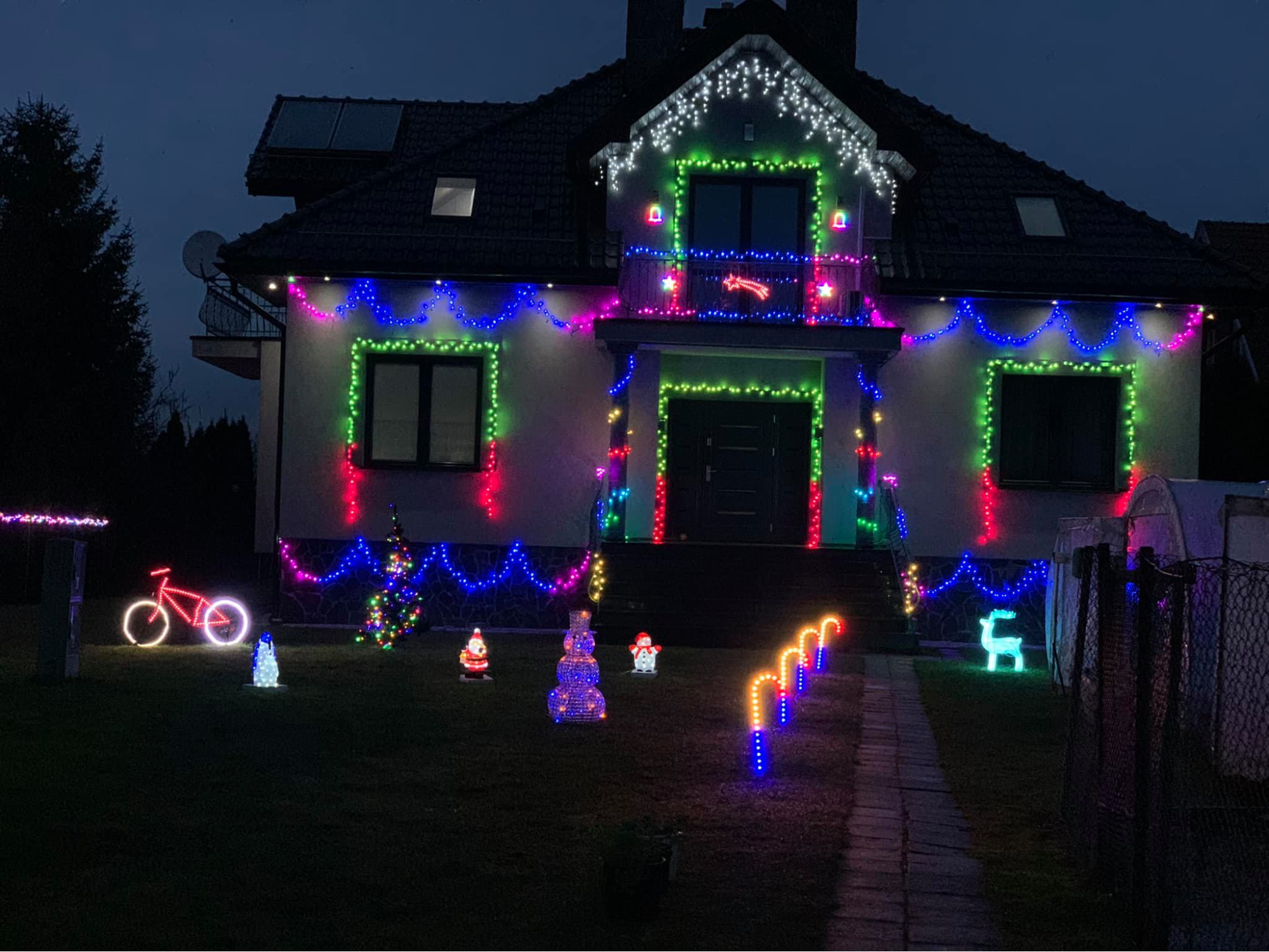
The website users control the lights. You can turn them on and off. My installation (A secret haven) consists of 20 sets of LED lamps consisting of about 2,000 lights. Not counting those hung on the Christmas tree at home. The whole can be admired by cameras transmitting live images.

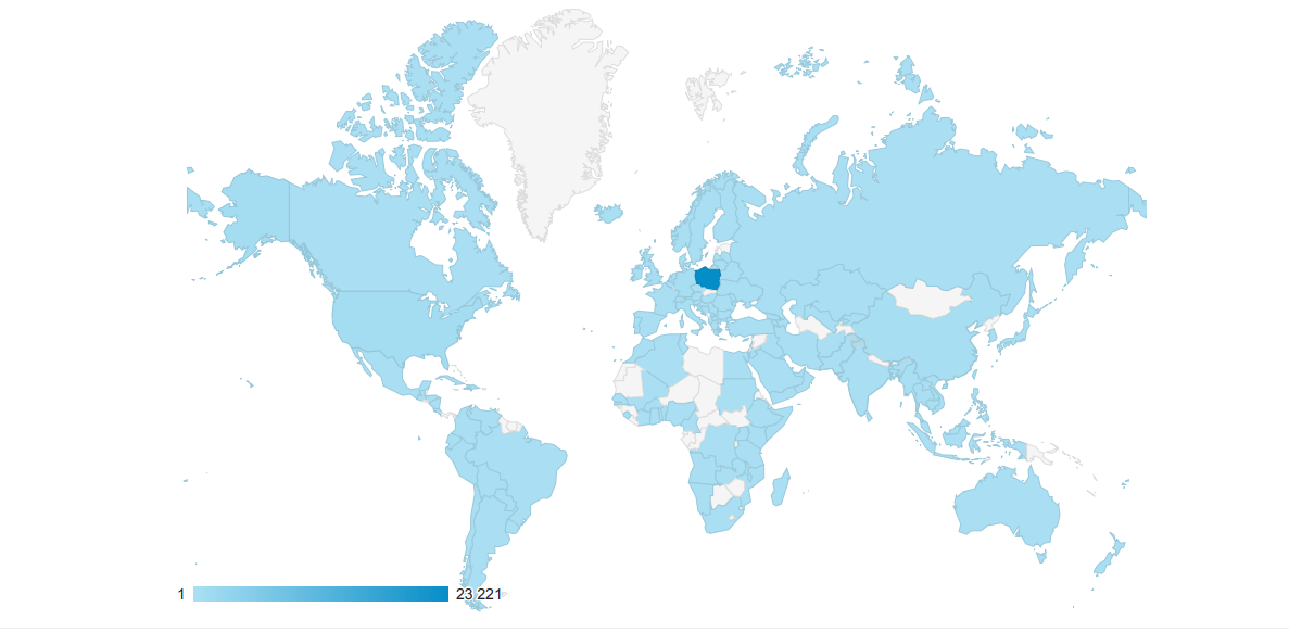
The project enjoys increasing popularity year by year, which translates into the number of visits to the website. We have entries from virtually all over the world.

The start of the two main controls is scheduled for Christmas Eve. Programmable LEDs will be used to present the illumination, and their control will consist in selecting musical sequences to the rhythm of which the lighting will turn on.

Additionally, this year we decided to provide users with an innovative facility, and we connected a receipt printer to our Discord channel. The camera was directed at the printer. It turned out to be an incredible hit because users are eager to write messages in a shared chat and watch them print live 🙂

The idea of sharing a printer was completely spontaneous. For this task, we wanted to choose a printer that would be as maintenance-free as possible. After reviewing many offers, we chose the Epson TM-T88IV printer. This printer supports the ESC / POS standard, so you can “write” to it using many libraries available on the web.

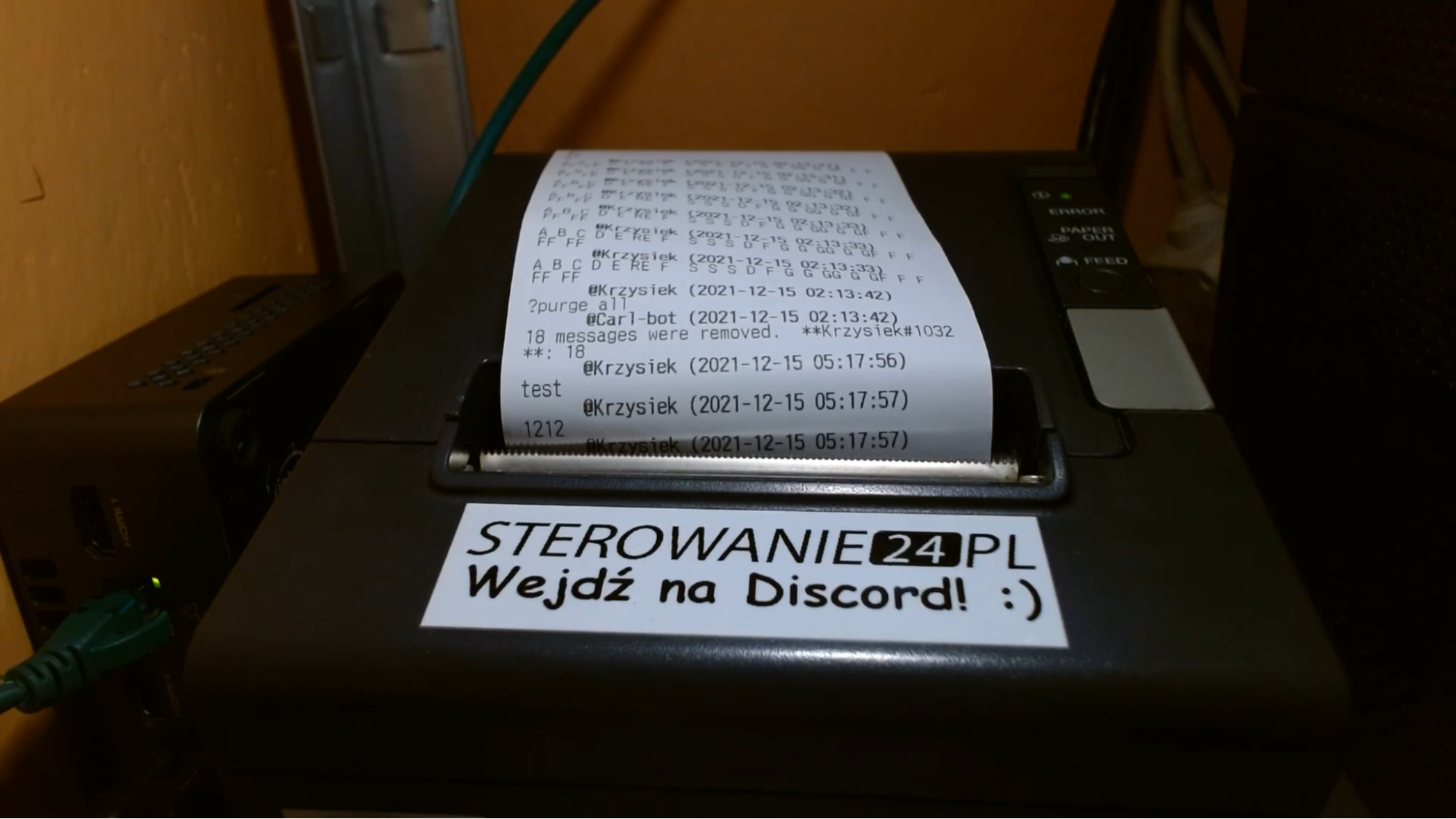
Our proprietary script, using the DiscordPHP library, is responsible for sending messages from Discord to the printer. An appropriate message is generated and sent to RabbitMQ.

Our proprietary code is also responsible for sending messages from Tipply, which also was handled with RabbitMQ. We use RabbitMQ to queue outgoing messages to the printer. The printer is connected to the computer via an RS232 port, which might not keep up with a large amount of messages – this is why we queue messages.

We would like to invite all Internet users to play with our installation, and people who would like to join the project, please contact us.

Tomasz Siron (26) – Originator and initiator of Smartpixels.app. Responsible for technical, architectural, and public relations issues of the project. A graduate of Mechatronics at the Lublin University of Technology. Currently an administrator and enthusiast of Linux systems in the Lublin (Poland) branch of an IT industry company. Passionate about electronics, computer science, and broadly understood science. He loves to DIY, is the author of one of the most popular polish Facebook groups, “Majsterkowanie dla każdego”.

PIEEG — A Low-Cost, Raspberry Pi Based Brain-Computer Interface

The study of the electrical waves within the brain as a check for seizure activity relating to sleep disorders, brain tumors or epilepsy, has resulted in a parallel need for affordable EEG-based consumer applications in the healthcare center.

Electronics, EEG, BCI, and neutral network Expert, Ildar Rakhmatulin and Co, have started working on a low-cost EEG device aimed at converting your Raspberry Pi 3 or Raspberry Pi 4 into a brain-computer interface (BCI). The PIEEG is an open-source device designed for reading the brain signals through the EEG signals onto a computer for processing, storage, or transmission.

According to Rakhmatulin on Github,

“the project is the result of several years of work on the development of BCI. We believe that the easiest way to get started with biosignals is to use a shield.”

The PIEEG is a board that fits the GPIO header of Raspberry Pi SBC and connects the SBC to head-worn EEG electrodes to read minute brain impulses (waves) through the scalp, amplifying them for processing, exchange, and visualization on a monitor. The device is furnished with a TCPIP protocol to allow for wireless operations in terms of data transfer from the device and comfortable movement by the user at daily usage. The project also has an onboard noise suppression system that improves the accuracy of measurements and recordings.

At setup, you need to connect the board called shield to your Raspberry Pi SBC (which must be battery-powered), followed by your electrodes. The monitor, for visualization, must also be powered by the Raspberry Pi and you should ensure complete isolation from the mains supply. You should also try to wear insulated shoes to ensure isolation with the earth and increased resistance for best reading while carrying out measurement, as non-insulated shoes will cause increased noise interference footprints. Finally, ensure you use the right pinout: 43: +5V, 44: GND, 37: MOSI, 34: MISO, 35: CLKL and 36: CS for the shield interface with the Raspberry Pi.

At the moment, noise measures of the system taken in real-time via timeflux have been made on Internal Short Circuit; Chewing Artifact; Blinking Artifact, After Chewing; and Alpha Wave Detection With Eyes Open, Eyes Closed and there is a good measurement.

The device supports software for signal reading, processing, and visualization. While C/C++ scripts are required for data reading, Python is needed for signal processing and visualization. Source code and specification on how to build the EEG device is given on Rakhmatulin’s Github repository if you would like to work on a similar project.

LoRa Hat Expansion For Raspberry Pi Starts at $40

Known for its DIY Robots and Hats for single board computers, SB Components has launched a crowdfunding campaign for its newest devices, LoRa Modules 868/433/915MHz — a LoRa HAT for Raspberry Pi and a LoRa Expansion for Pico, designed for data transmission of up to 5km with low power consumption, and support for auto repeating capability.

The LoRa HAT for Raspberry Pi incorporates Ebyte’s E22-900T22S/E22-400T22S serial port module with 915/868/433MHz band and a Semtech SX1262/SX1268 module for its enhanced data communication in low power consumption. The HAT supports a 22dBm signal power with a range of up to 5km. The board features a 74HC125V voltage level translator, a UART communication interface, a wireless parameter config support, and a USB to LoRa and Pico to LoRa communication through a UART. The LoRa HAT for Raspberry Pi also features fixed-point transmission support, and SMA and IPEX antenna connector, and a support protocol for evaluating signal quality via the RSSI (Received Signal Strength Indicator).

Additionally, the board offers a Wake on Radio and Deep Sleep Mode to drive its installed applications and solutions in low-power consumption (a feature already mentioned). The LoRa HAT debuts a 40-pinout header including 3x GPIOs; 4x Power; 7x Ground; and 2x UART interfaces, a USB, and an antenna connector.

The LoRa Expansion for Pico board is based on the same E22 module, adding a pre-soldered Raspberry Pi and a 1.14-inch LCD, maintaining the same features as the LoRa HAT for Raspberry Pi.

Key Features and Specifications of LoRa HAT for Raspberry Pi and LoRa Expansion for Pico:

  • Serial Port module:
    • Ebyte E22-900T22S based on SX1262 @ 850 – 930 MHz band
    • Ebyte E22-400T22S based on SX1268 @ 410 – 493MHz band
  • Supported frequencies: 433 MHz / 868 MHz / 915 MHz
  • Range: Up to 5 km
  • SMA antenna connector
  • 1x Micro USB
  • UART, GPIOs via 40-pin header, 74HC125V voltage level translator
  • LED: Indicators for Tx/Rx, AUX, and power
  • Serial/USB selection Jumpers:
    • Control Raspberry Pi with USB to UART (serial)
    • Control Raspberry Pi Pico with USB

There is no mention of particular software for the boards, but that shouldn’t be a big deal since Ebyte E32 has compatibility with Raspberry Pi in existing projects. So, we can say there is software to start with, but maybe with some tweaking. The Ebyte LoRa E22 library with acclaimed compatibility with all architectures including the Arduino and ESP32.SX1262/SX1268 could also be useful.

The LoRa 868/433/915MHz module is available on Kickstarter with four (4) rewards starting from $40 to $1,325 and more. Its campaign will end on Monday, January 3, 2022, for shipping to commence by February 2022. After the campaign, you’ll be asked your preferred frequency like 433/868/915 Mhz and the company will provide you with the corresponding antenna.

“If anyone wants LoRa HAT for Pi in different frequencies then they can mark that frequency at the time of the survey,”

says Ashish.

The campaign also offers add-ons that you can use with the LoRa HAT. The duo mode is said to support communication between one another as I quote Ashish Kumar saying,

“the Lora HAT works with the LoRa network designed to make the communication easy in economical range. Yes, you should have two LoRa so that they can communicate with each other. We also provided addons HAT in the add-on section that you can use with LoRa HAT. Yes, you can communicate with pico Lora expansion and LoRa HAT for Pi or vice versa.”

Other useful information on the SB component’s device can be found on Kickstarter‘s page.

TOP PCB Companies